 | –≠–ª–µ–∫—Ç—Ä–æ–Ω–Ω—ã–π –∫–æ–º–ø–æ–Ω–µ–Ω—Ç: STV6688 | –°–∫–∞—á–∞—Ç—å:  PDF PDF  ZIP ZIP |
PRODUCT PREVIEW
STV6688
Video Switch Matrix for TV Applications with S Terminal
Æ
This is preliminary information on a new product now in development. Details are subject to change without notice.
September 2003
1/12
Key Features
s
I≤C Bus Control
s
Standby Mode
s
4 Y/CVBS Inputs (one for internal TV signal)
s
4 C Inputs (one for internal TV signal)
s
1 Y/C Adder
s
1 Y/CVBS and 1 C Output, each with 0 dB gain
s
1 CVBS Output with 6 dB gain and 150
Buffer for Monitor
s
SYNC Bottom Clamp on all CVBS/Y and
Average Bias on C Inputs
s
Bandwidth: 15 MHz
s
Crosstalk: 50 dB (min.)
General Description
The STV6688 is a highly-integrated I≤C bus-
controlled video switch matrix, optimized for use in
color TV applications.
It is used to control the switching of 4 video signals.
These signals can be in Single Component form
(CVBS) or in Two Component form (Y/C). In both
cases, the STV6688 microcontroller provides a
CVBS signal for an external device (monitor).
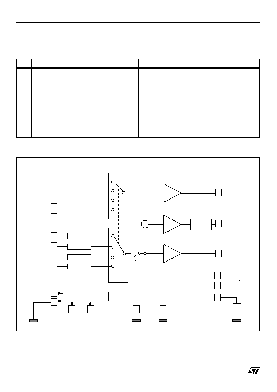
Pin Connections
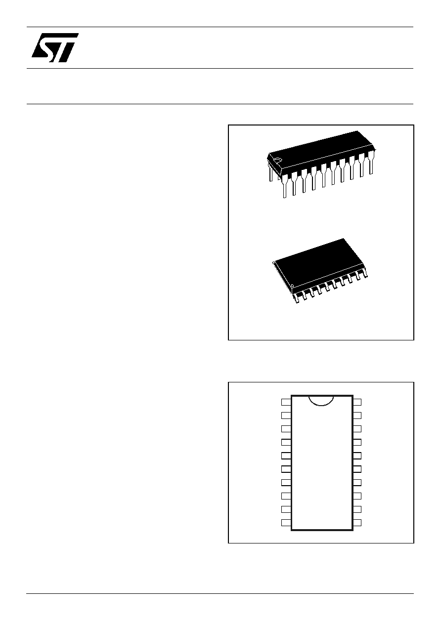
Order Code: STV6688
PDIP20
Order Code: STV6688A
PSO20
1
2
3
4
5
6
7
8
9
10
20
19
18
17
16
15
14
13
12
11
Y/CVBS_IN1
C_IN1
VCC_V
Y/CVBS_IN2
C_IN2
GND_V
Y/CVBS_IN3
C_IN3
VDD
SDA
DEC
Y/CVBS_IN_TV
C_IN_TV
VCC_B
CVBS_OUT
GND_B
Y/CVBS_OUT
C_OUT
GND
SCL
Functional Description
STV6688
2/12
1
Functional Description
Table 1: Pin List
Pin
Symbol
Description
Pin
Symbol
Description
1
Y/CVBS_IN1
Y or CVBS Signal of Ext. Input 1
11
SCL
Serial Clock Line Input
2
C_IN1
C Signal of Ext. Input 1
12
GND
Digital Parts Ground
3
VCC_V
Video Switch Power Supply
13
C_OUT
C Signal Output
4
Y/CVBS_IN2
Y or CVBS Signal of Ext. Input 2
14
Y/CVBS_OUT
Y/CVBS Output
5
C_IN2
C Signal of Ext. Input 2
15
GND_B
Buffer Ground
6
GND_V
Video Switch Ground
16
CVBS_OUT
Y and C Adder Output
7
Y/CVBS_IN3
Y or CVBS Signal of Ext. Input 3
17
VCC B
Buffer Power Supply
8
C_IN3
C Signal of Ext. Input 3
18
C_IN_TV
C Signal of TV Input
9
VDD
Digital Parts Power Supply
19
Y/CVBS_IN_TV
Y or CVBS Signal of TV Input
10
SDA
Serial Data Line Input
20
DEC
Decoupling
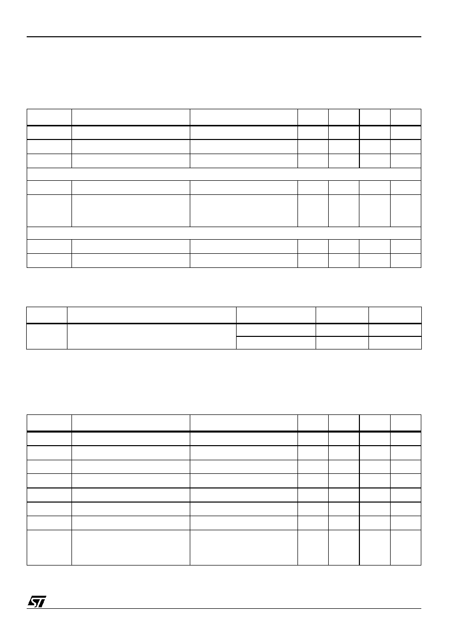
Figure 1: STV6688 Block Diagram
+
6dB
Buffer
I≤C Bus Decoder
Y/CVBS_IN1
Y/CVBS_IN2
Y/CVBS_IN3
C_IN TV
C_IN1
C_IN2
C_IN3
V
DD
GND
SDA
SCL
GND B
GND V
DEC
V
CC
V
V
CC
B
C_OUT
CVBS_OUT
Power
Video
Power
Buffer
Supply
Supply
0dB
Y/CVBS_IN TV
Y/CVBS_OUT
Mute
V
REF
19
1
4
7
9
12
10
11
6
15
20
3
17
13
16
14
0dB
Clamp
Clamp
Clamp
Clamp
18
2
5
8
3/12
STV6688
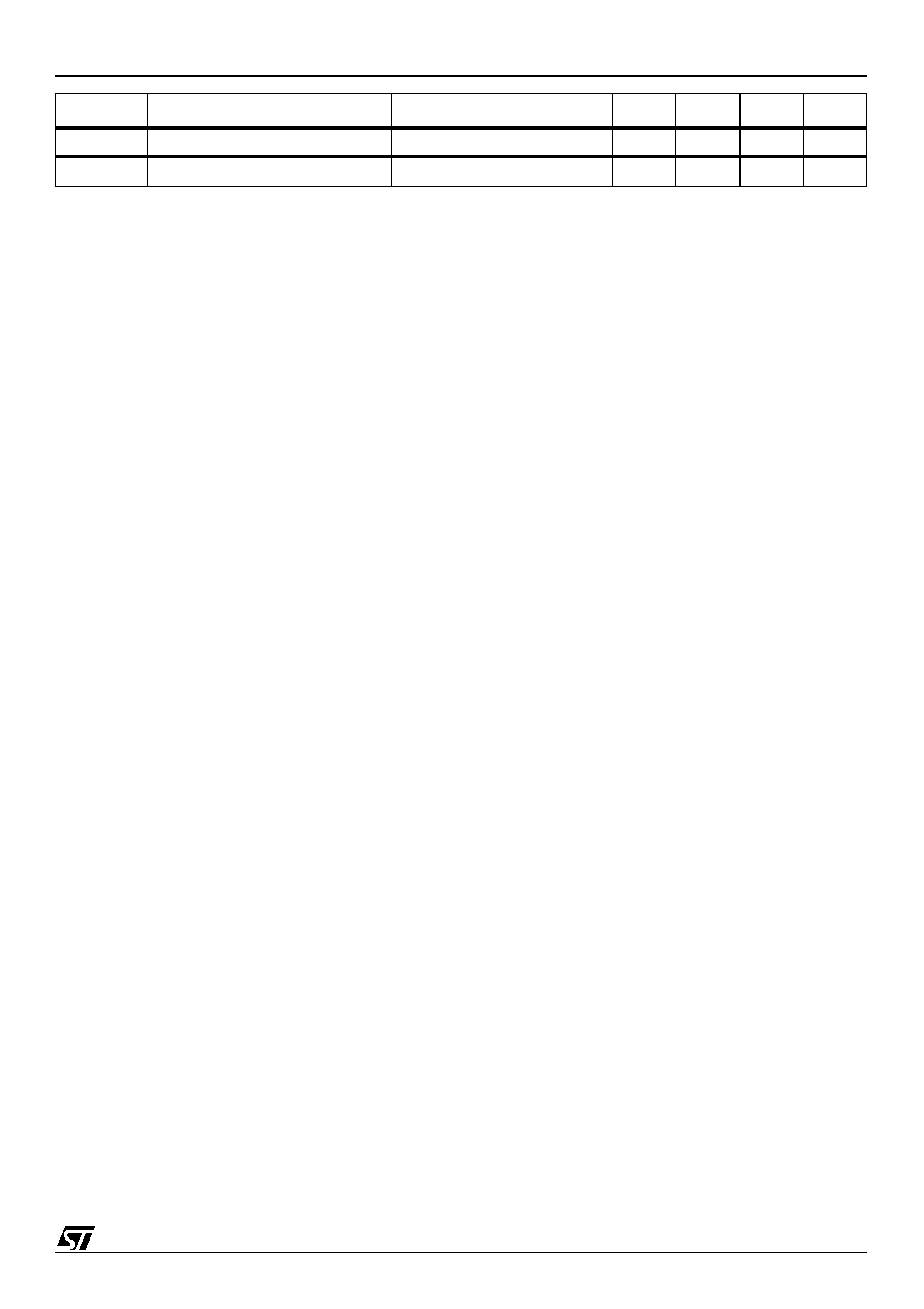
Electrical Characteristics
2
Electrical Characteristics
T
AMB
= 25∞C, V
CCV
= V
CCB
= V
DD
= 5V, R
LoadYC
= 4.7 k
,
R
LoadCVBS
= 150
, unless otherwise
specified.
2.1
Thermal Data
2.2
Y/CVBS Section
T
AMB
= 25∞C, V
CCV
= V
CCB
= V
DD
= 5V, R
LoadYC
= 4.7 k
,
R
LoadCVBS
= 150
, unless otherwise
specified.
Symbol
Parameter
Test Conditions
Min.
Typ.
Max.
Unit
V
DD
Digital Supply Voltage
4.5
5
5.5
V
V
CC
Video Operating Supply Voltage
4.5
5
5.5
V
V
CCB
Buffer Supply Voltage
4.5
5
5.5
V
Active (Channels ON)
I
DD
Digital Supply Current
V
DD
= 5 V
3
mA
I
CCV
Total Video Supply Current
(V
CC,
V
CCBi
)
V
CC
= 5 V, No load
V
CCV
= V
CCB
= 5V, with loads and
signals
13
25
mA
Standby (All Channels OFF)
I
DD
Digital Supply Current
V
DD
= 5 V
3
mA
I
CCVstd
Total Video Supply Current
V
CC
= 5 V
0.3
mA
Symbol
Parameter
Package
Value
Unit
R
thJA
Maximum Junction-to-Ambient Thermal Resistance
DIP20 (STV6688)
80
∞C/W
SO20 (STV6688A)
100
∞C/W
Symbol
Parameter
Test Conditions
Min.
Typ.
Max.
Unit
V
DCIN
DC Input Level
Bottom Sync pulse
2
V
I
CLAMP
Clamping Current
at V
DCIN
-400 mV
1
2
mA
I
LEAK
Input Leakage Current
V
IN
= V
DCIN
+ 1 V
1
10
µ
A
C
IN
Input Capacitance
2
pF
V
IN
Max Input Signal
V
CC
= 5 V
1.5
V
PP
DYNY
Dynamic Y/CVBS Output Signal
V
CC
= 5 V
1.5
V
PP
DYNCVBS
Dynamic CVBS Output Signal
V
CC
= 5 V
3
V
PP
BW
Bandwidth at -3 dB
Y/CVBS
Y/C Mixer (on CVBS_OUT)
V
IN
= 1 V
PP
V
IN
= 1 V
PP
12
8
15
10
MHz
Electrical Characteristics
STV6688
4/12
Note: 1 S/N = 20log (V
OUT
Black to White = 0.7 V
PP
/V
Noise
(mV
RMS
) weighted CCIR567).
2.3
Chroma Section
T
AMB
= 25∞C, V
CCV
= V
CCB
= V
DD
= 5V, R
LoadYC
= 4.7 k
,
R
LoadCVBS
= 150
, unless otherwise
specified.
Flatness
Spread of Gain in Video Band
(15 kHz-5 MHz)
Y/CVBS
Y/C Mixer (on CVBS_OUT)
V
IN
= 1 V
PP
V
IN
= 1 V
PP
±0.2
±0.5
±0.5
±1.0
dB
CTi
Crosstalk Isolation between
Y/CVBS Input Channels
V
IN
= 1 V
PP
at f = 4.43 MHz, on
one point.
55
60
dB
CTo
Crosstalk Isolation of Y/CVBS from C
Channels
V
IN
= 1 V
PP
at f = 4.43 MHz, on
one point.
50
55
dB
GYCVBS
Gain at Y/CVBS out @1 MHz
V
IN
= 1 V
PP
-0.5
0
+0.5
dB
GCVBS
Gain at CVBS out @1 MHz
V
IN
= 1 V
PP
5.5
6
6.5
dB
R
OUTY
Y/CVBS Output Resistance
2.5
5.0
R
OUTCVBS
CVBS Output Resistance
1
5
G
YCVBSM
Gain matching between Y, CVBS
inputs
V
IN
= 1 V
PP
-0.5
0
+0.5
dB
DC
OUTCVBS
DC CVBS Output voltage
Bottom sync pulse
0.8
V
DC
OUTY
DC Y Output voltage
Bottom sync pulse for Y
1.3
V
DPHI
Differential Phase
V
IN
= 1 V
PP
at f = 4.43 MHz
1
3
deg
DG
Differential Gain
V
IN
= 1 V
PP
at f = 4.43 MHz
1
5
%
LNL
Luminance non-linearity
0.6
3
%
VSN
Video S/N ratio
Refer to
Note 1
65
dB
Symbol
Parameter
Test Conditions
Min.
Typ.
Max.
Unit
V
DCIN
DC Input Level
3
V
R
IN
Input Resistance
30
50
k
C
IN
Input Capacitance
2
pF
V
IN
Max Input Signal
1.5
V
PP
DYN
Dynamic Output Signal
1.5
V
PP
CBW
Chroma Bandwidth
C
IN
= 1 V
PP
10
12
MHz
CTi
Crosstalk Isolation between C Input
Channels
C
IN
= 0. 5V
PP
at f = 4.43 MHz, on
one point.
55
60
dB
CTo
Crosstalk Isolation of C from Y
Channels
V
IN
= 1 V
PP
at f = 4.43 MHz, on
one point.
50
55
dB
R
OUT
Output Resistance
2.5
5.0
G
OUTC
Gain at C_OUT @4.43 MHz
V
IN
= 1 V
PP
-0.5
0
+0.5
dB
DC
OUTC
DC Output voltage
2.2
V
Symbol
Parameter
Test Conditions
Min.
Typ.
Max.
Unit
5/12
STV6688
Electrical Characteristics
G
CM
Gain matching between C inputs
V
IN
= 1 V
PP
-0.5
0
+0.5
dB
CToYdel
Chroma to Luma delay, Y/C source
V
PP
@4.43 MHz
5
10
ns
Symbol
Parameter
Test Conditions
Min.
Typ.
Max.
Unit