This is preliminary information on a new product in development or undergoing evaluation. Details are subject to change without notice.
Version 4.1
August 2003
1/17
STV7617DU
PLASMA DISPLAY PANEL SCAN DRIVER
FEATURES
s
64/65 SELECTABLE OUTPUT PLASMA
DISPLAY DRIVER
s
100 V ABSOLUTE MAXIMUM SUPPLY
s
5 V SUPPLY FOR LOGIC
s
100/850 mA SOURCE/SINK OUTPUT
s
700 mA SOURCE/SINK OUTPUT DIODE
s
65-bit BIDIRECTIONAL SHIFT REGISTER
(8 MHz)
s
HIGH IMPEDANCE OUTPUT CONTROL
s
BCD TECHNOLOGY
s
100-PIN TQFP PACKAGE WITH
INTEGRATED HEATSINK
DESCRIPTION
The STV7617 is a scan driver for Plasma Display
Panel (PDP) implemented in ST's proprietary
BCD technology. Using a 65-bit cascadable
8 MHz shift register, it drives 65 high current &
high voltage outputs. The STV7617 can be config-
ured either in 64 or 65 outputs depending on the
SEL input Pin.
By serially connecting several STV7617, any ver-
tical pixel definition can be performed. The
STV7617 is supplied with a separated 90V power
output supply and a 5 V logic supply. All command
inputs are CMOS compatible. The STV7617 pack-
age is a 100-pin TQFP with integrated heatsink lo-
cated on the bottom (STV7617D) or top
(STV7617U) of the package. It is also available
without heatsink (STV7617).
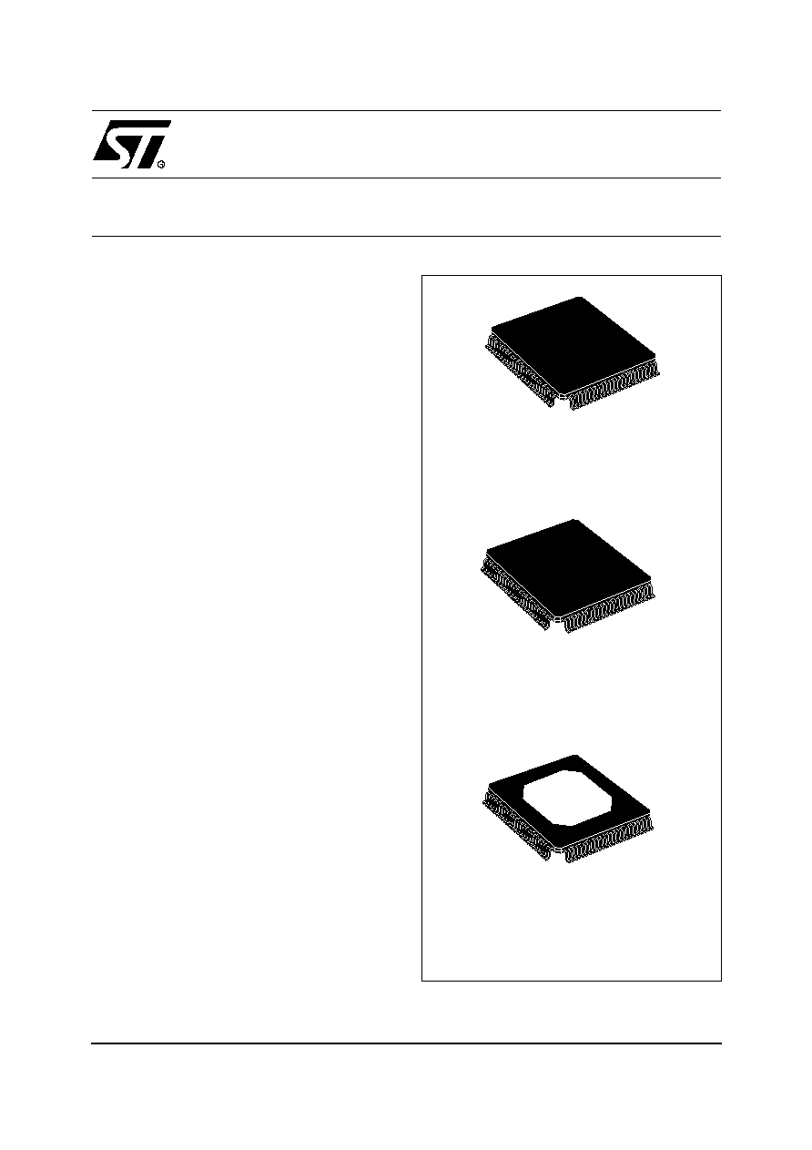
TQFP100 (14 x 14 x 1.4 mm Slug-down)
(Thin Plastic Quad Flat Pack)
ORDER CODE: STV7617D
TQFP100 (14 x 14 x 1.4 mm Slug-up)
(Thin Plastic Quad Flat Pack)
ORDER CODE: STV7617U
TQFP100 (14 x 14 x 1.4 mm)
(Thin Plastic Quad Flat Pack)
ORDER CODE: STV7617
1

TABLE OF CONTENTS
2
2/17
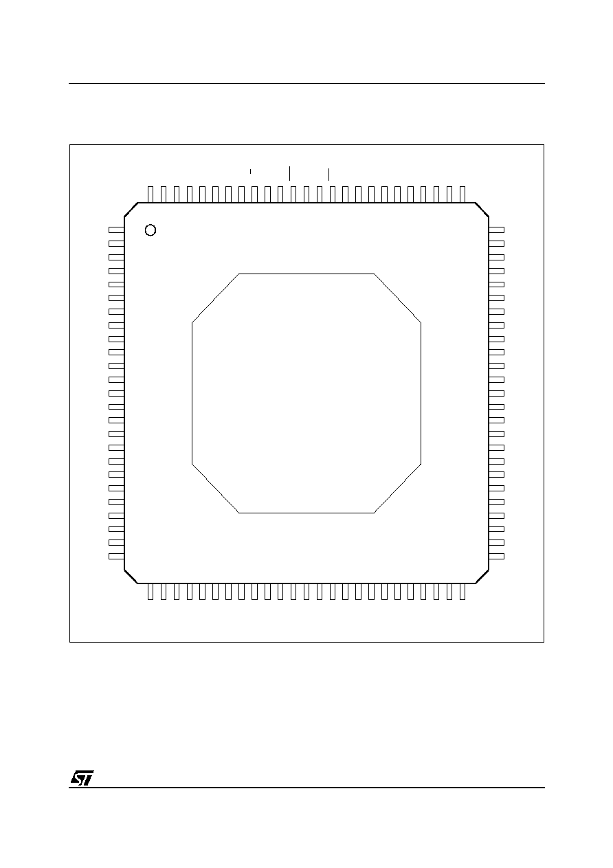
PIN CONNECTIONS (SLUG-UP) . . . . . . . . . . . . . . . . . . . . . . . . . . . . . . . . . . . . . . . . . . . . . . . . . . . 3
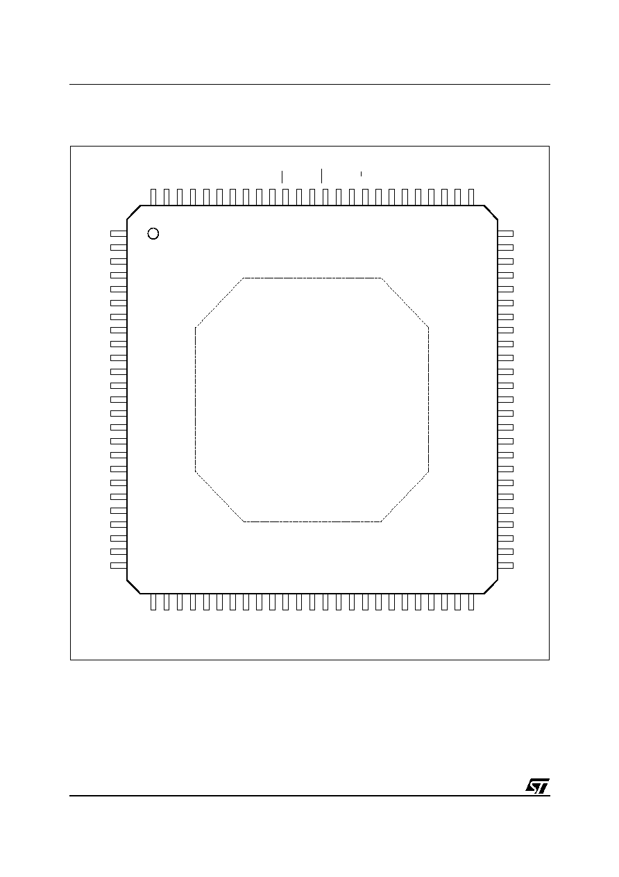
PIN CONNECTIONS (SLUG-DOWN) . . . . . . . . . . . . . . . . . . . . . . . . . . . . . . . . . . . . . . . . . . . . . . . 4
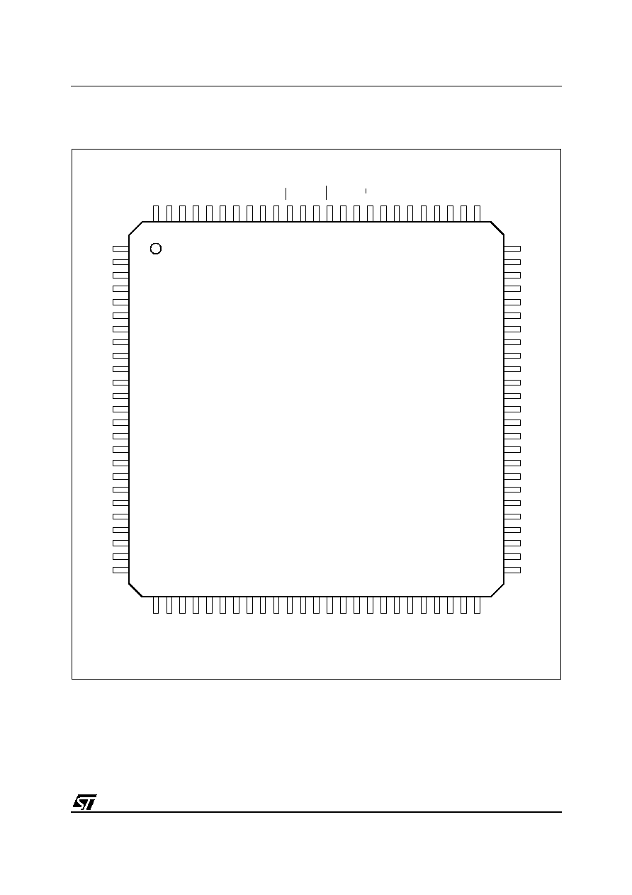
PIN CONNECTIONS (NO SLUG) . . . . . . . . . . . . . . . . . . . . . . . . . . . . . . . . . . . . . . . . . . . . . . . . . . . 5
PIN ASSIGNMENT . . . . . . . . . . . . . . . . . . . . . . . . . . . . . . . . . . . . . . . . . . . . . . . . . . . . . . . . . . . . . . 6
BLOCK DIAGRAM . . . . . . . . . . . . . . . . . . . . . . . . . . . . . . . . . . . . . . . . . . . . . . . . . . . . . . . . . . . . . . 7
CIRCUIT DESCRIPTION . . . . . . . . . . . . . . . . . . . . . . . . . . . . . . . . . . . . . . . . . . . . . . . . . . . . . . . . . 7
ABSOLUTE MAXIMUM RATINGS . . . . . . . . . . . . . . . . . . . . . . . . . . . . . . . . . . . . . . . . . . . . . . . . . 8
THERMAL DATA . . . . . . . . . . . . . . . . . . . . . . . . . . . . . . . . . . . . . . . . . . . . . . . . . . . . . . . . . . . . . . . 8
ELECTRICAL CHARACTERISTICS . . . . . . . . . . . . . . . . . . . . . . . . . . . . . . . . . . . . . . . . . . . . . . . . 9
AC TIMING REQUIREMENTS . . . . . . . . . . . . . . . . . . . . . . . . . . . . . . . . . . . . . . . . . . . . . . . . . . . . 10
AC TIMING CHARACTERISTICS . . . . . . . . . . . . . . . . . . . . . . . . . . . . . . . . . . . . . . . . . . . . . . . . . 10
INPUT/OUTPUT CHARACTERISTICS . . . . . . . . . . . . . . . . . . . . . . . . . . . . . . . . . . . . . . . . . . . . . 13
PACKAGE MECHANICAL DATA (SLUG-DOWN) . . . . . . . . . . . . . . . . . . . . . . . . . . . . . . . . . . . . 14
PACKAGE MECHANICAL DATA (SLUG-UP) . . . . . . . . . . . . . . . . . . . . . . . . . . . . . . . . . . . . . . . 15
PACKAGE MECHANICAL DATA (NO SLUG) . . . . . . . . . . . . . . . . . . . . . . . . . . . . . . . . . . . . . . . 16
2