April 2002
1/16
This is preliminary information on a new product now in development. Details are subject to change without notice.
Version 3.1
STV7620
PLASMA DISPLAY PANEL DATA DRIVER
PRELIMINARY DATA
FEATURES
s
96 Outputs Plasma Display Driver
s
90V Absolute Maximum Rating
s
Reduced EMI (Electro Magnetic Interference)
s
3.3V / 5V Compatible Logic
s
-40 / 30 mA Source / Sink Output Mos
s
6 Bit Data Bus (40 MHz)
s
BCD Process
s
Packaging Adapted to Customer Request
(DICE, COB, COF, TAB).
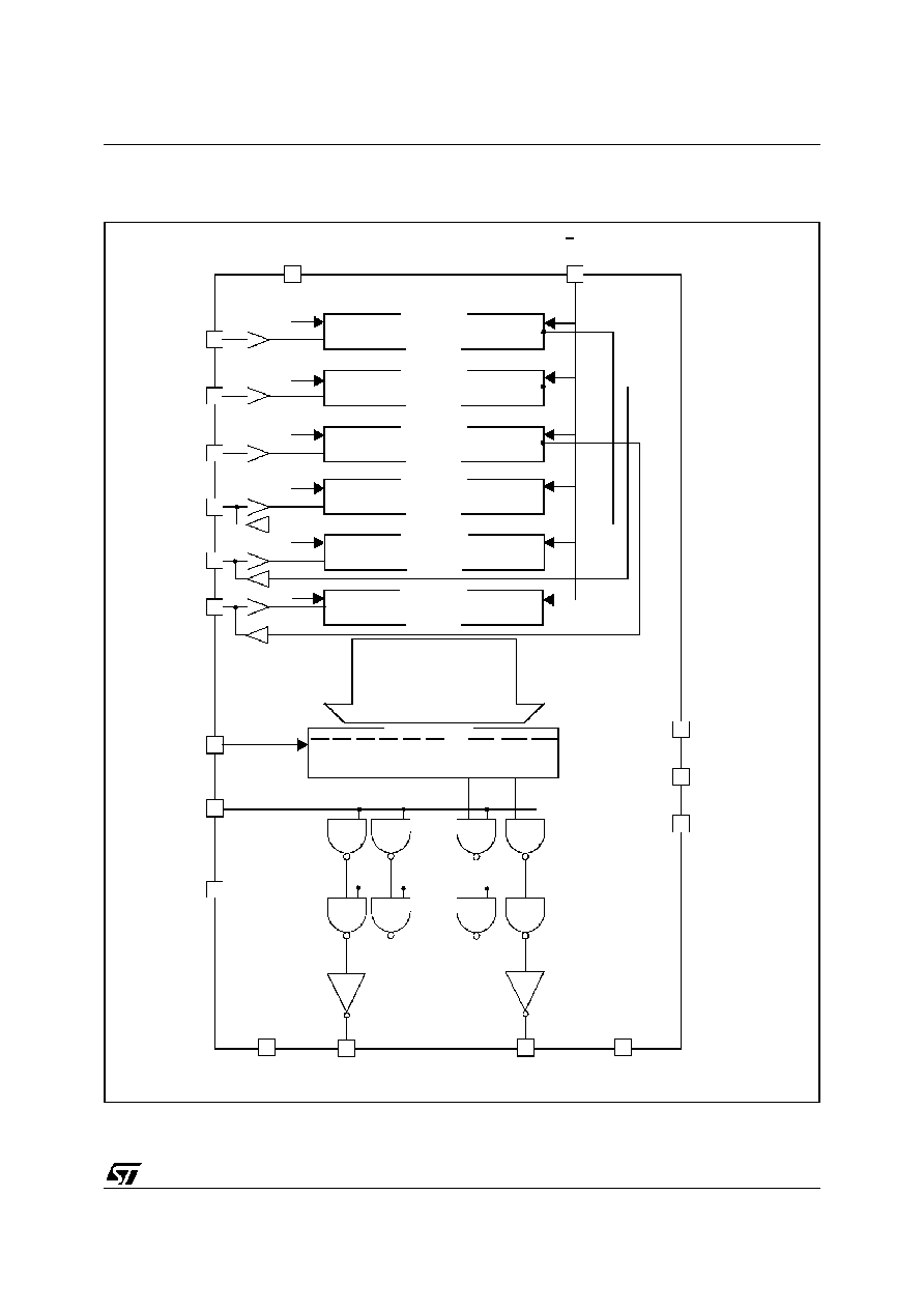
DESCRIPTION
STV7620S/M/F is a data driver for Plasma Display
Panel (PDP) designed in the ST proprietary BCD
high voltage technology. A new shape of the out-
put pulse generated by the STV7620S/M/F en-
sures a noticeable EMI reduction. Three different
versions are available with various falling edge
shapes. Using a 6 bit wide data bus, they can con-
trol 96 high current & high voltage outputs. The
STV7620S/M/F is supplied with a separated 70V
power output supply and a 5V logic supply. All
command inputs are CMOS and 3.3V logic levels
compatible.
Please contact STMicroelectronics for ordering
information concerning samples or bump version
(1) refer to timing characteristics (Section 10)
Order code (1)
Version
STV7620S
slow speed
STV7620M
medium speed
STV7620F
fast speed
1

STV7620S/M/F
2/16
Revision follow-up
Target specification
02/2001
version 1.0
document creation
03/2001
version 1.1
general update, addition of EMI and figure 1
04/2001
version 1.2
general update, new pads dimensions
10/2001
version 1.3
addition of die photo in cover page, new pads dimensions
Electrical characteristics: replaced a few TBD mentions with values
AC timing characteristics: some TBD replaced with values
F/R replaced with F/R
Electrical characteristics: Idoutl/h value replaced with
�
30mA
Preliminary data
02/2002
version 3.0
whole document: sales type becomes STV7620S/M/F for slow, medium, fast
general update
04/02/2002
Version 3.1
general update
2
STV7620S/M/F
5/16
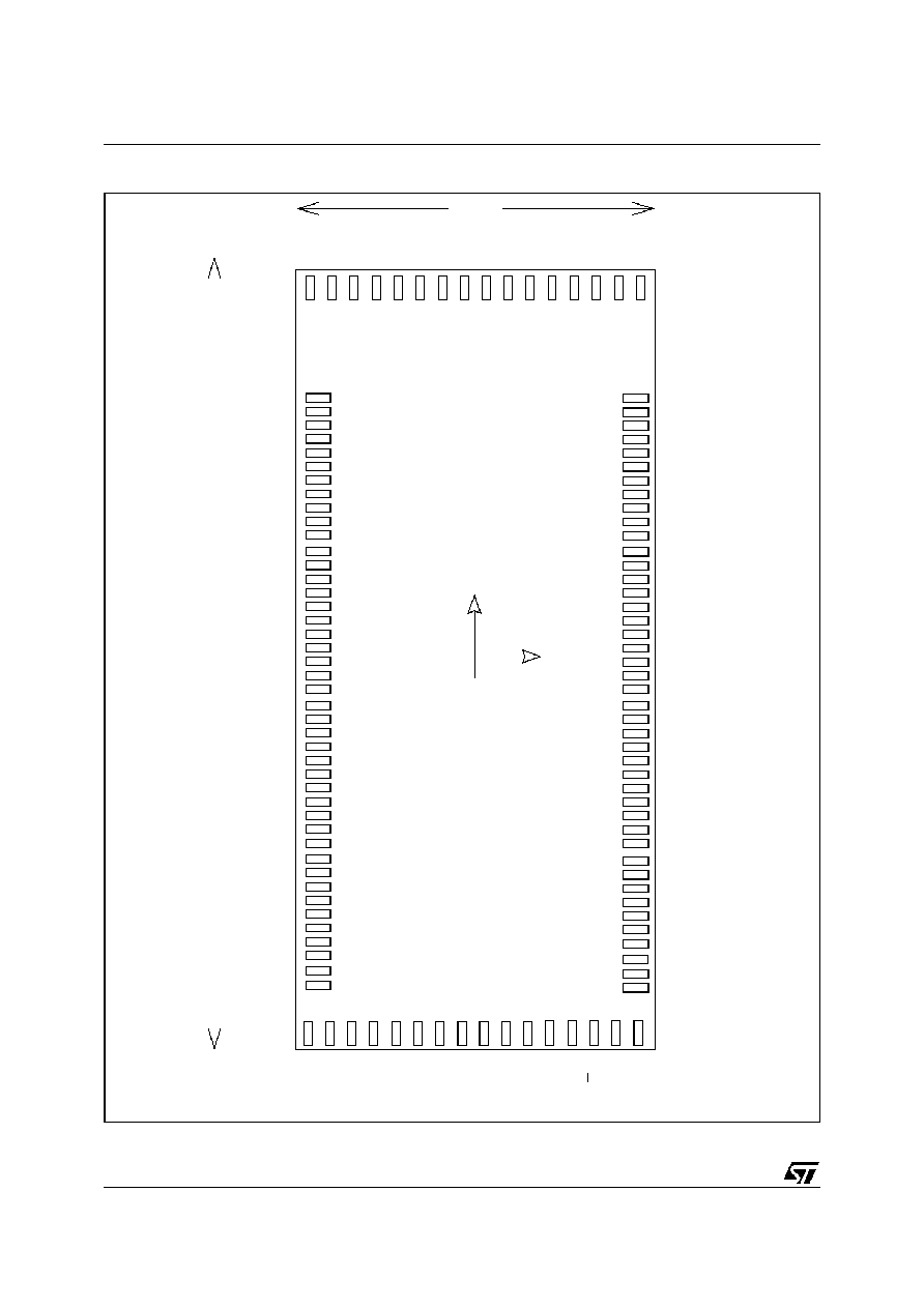
3
PADS DIMENSIONS (in
�
m)/ PADS POSITIONS
The reference is the centre of the die (x=0, y=0)
Pad size is specified for wire-bonding options
.
TOP SIDE from left to right
Name
Centre:X
Centre:Y
Size:x
SIze: y
OUT56
-774.478
2696.03
76
92
OUT55
-671.288
2696.03
76
92
OUT54
-568.098
2696.03
76
92
OUT53
-464.907
2696.03
76
92
OUT52
-361.718
2696.03
76
92
OUT51
-258.528
2696.03
76
92
OUT50
-155.338
2696.03
76
92
OUT49
-52.148
2696.03
76
92
OUT48
51.042
2696.03
76
92
OUT47
154.232
2696.03
76
92
OUT46
257.422
2696.03
76
92
OUT45
360.612
2696.03
76
92
OUT44
463.802
2696.03
76
92
OUT43
566.992
2696.03
76
92
OUT42
670.267
2696.03
76
92
OUT41
773.457
2696.03
76
92
BOTTOM SIDE from right to left
Name
Centre:X
Centre:Y
Size:x
SIze: y
VSSLOG
770.822
-2696.03
76
92
CLK
670.352
-2696.03
76
92
F/R
567.162
-2696.03
76
92
POC
463.972
-2696.03
76
92
VCC
360.782
-2696.03
76
92
STB
258.442
-2696.03
76
92
BLK
155.252
-2696.03
76
92
A1
52.062
-2696.03
76
92
A2
-51.128
-2696.03
76
92
A3
-154.318
-2696.03
76
92
A4
-257.508
-2696.03
76
92
A5
-360.698
-2696.03
76
92
A6
-463.888
-2696.03
76
92
VSSSUB
-567.078
-2696.03
76
92
VSSLOG
-670.352
-2696.03
76
92
VSSLOG
-770.822
-2696.03
76
92
RIGHT SIDE from top to bottom
Name
Centre:X
Centre:Y
Size:x
SIze: y
OUT40
887.655
1950.792
92
76
OUT39
887.655
1847.602
92
76
OUT38
887.655
1744.327
92
76
OUT37
887.655
1641.138
92
76
OUT36
887.655
1537.947
92
76
OUT35
887.655
1434.757
92
76
OUT34
887.655
1331.568
92
76
OUT33
887.655
1228.378
92
76
OUT32
887.655
1125.188
92
76
OUT31
887.655
1021.998
92
76
OUT30
887.655
918.807
92
76
OUT29
887.655
815.618
92
76
OUT28
887.655
712.428
92
76
OUT27
887.655
609.238
92
76
OUT26
887.655
506.048
92
76
OUT25
887.655
402.857
92
76
OUT24
887.655
299.668
92
76
OUT23
887.655
196.478
92
76
OUT22
887.655
93.288
92
76
OUT21
887.655
-9.902
92
76
OUT20
887.655
-113.092
92
76
OUT19
887.655
-216.282
92
76
OUT18
887.655
-319.472
92
76
OUT17
887.655
-422.662
92
76
OUT16
887.655
-525.852
92
76
OUT15
887.655
-629.042
92
76
OUT14
887.655
-732.232
92
76
BOTTOM SIDE from right to left
Name
Centre:X
Centre:Y
Size:x
SIze: y