August 2003
1/19
STV7710/WAF
Vacuum Fluorescent Display (VFD) Driver
Æ
FEATURES
s
96 Outputs VFD Driver
s
90V Absolute Maximum Supply
s
3.3V/5V compatible logic
s
-40/30mA source/sink output MOS
s
-50/50mA source/sink output diode
s
1 bit data bus (40MHz)
s
BCD process
s
Packaging: Die Form
DESCRIPTION
STV7710/WAF is a driver for vacuum fluorescent
display (VFD) designed in the ST proprietary BCD
high voltage technology. Using a 1 bit wide data
bus, it can control 96 high current & high voltage
outputs. The STV7710/WAF is supplied with a
separated 70V power output supply. All command
inputs are CMOS and 3.3V logic levels compatible.
ORDERING INFORMATION
Ordering code
Package
STV7710/WAF
Bare die

STV7710/WAF
2/19
Table of content
Chapter 1
BLOCK DIAGRAM . . . . . . . . . . . . . . . . . . . . . . . . . . . . . . . . . . . . . . . . . . . . . . . . .3
Chapter 2
DIE PIN OUT / DIE DESCRIPTION . . . . . . . . . . . . . . . . . . . . . . . . . . . . . . . . . . . . .4
Chapter 3
MECHANICAL SPECIFICATION . . . . . . . . . . . . . . . . . . . . . . . . . . . . . . . . . . . . . .5
3.1
Alignment marks specification .............................................................................................. 5
3.2
Pads specification ................................................................................................................ 5
Chapter 4
CIRCUIT DESCRIPTION . . . . . . . . . . . . . . . . . . . . . . . . . . . . . . . . . . . . . . . . . . . . .9
4.1
Pin description ...................................................................................................................... 9
4.2
Data bus configuration ......................................................................................................... 9
4.3
Description ......................................................................................................................... 10
Chapter 5
ABSOLUTE MAXIMUM RATINGS . . . . . . . . . . . . . . . . . . . . . . . . . . . . . . . . . . . .11
Chapter 6
ELECTRICAL CHARACTERISTICS . . . . . . . . . . . . . . . . . . . . . . . . . . . . . . . . . . .12
Chapter 7
AC TIMING REQUIREMENTS . . . . . . . . . . . . . . . . . . . . . . . . . . . . . . . . . . . . . . . .13
Chapter 8
AC TIMING CHARACTERISTICS . . . . . . . . . . . . . . . . . . . . . . . . . . . . . . . . . . . . .14
Chapter 9
INPUT/OUPUT SCHEMATICS . . . . . . . . . . . . . . . . . . . . . . . . . . . . . . . . . . . . . . .17
Chapter 10
THERMAL CHARACTERISTICS . . . . . . . . . . . . . . . . . . . . . . . . . . . . . . . . . . . . .18
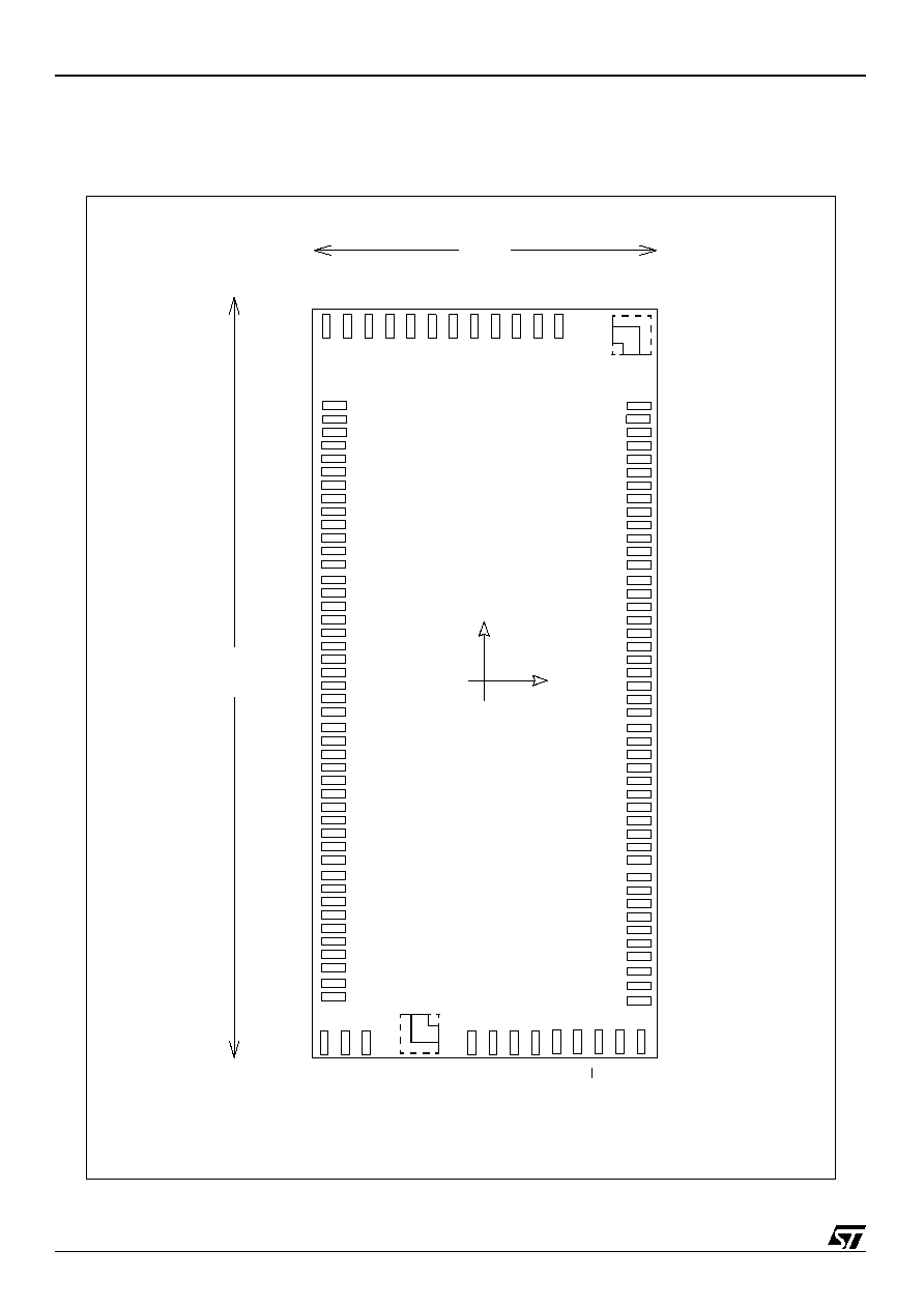
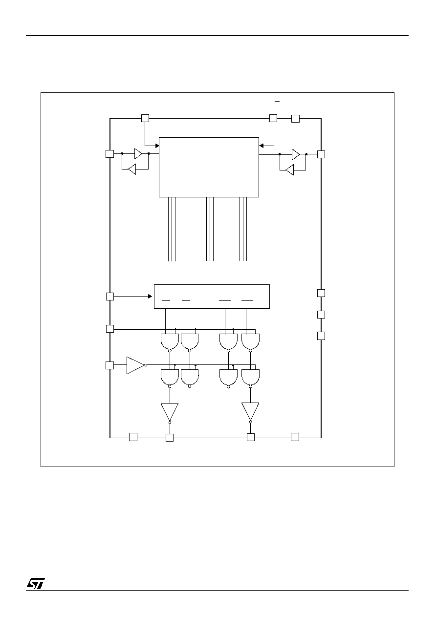
DIE PIN OUT / DIE DESCRIPTION
STV7710/WAF
4/19
2
DIE PIN OUT / DIE DESCRIPTION
Figure 2: STV7710/WAF die pinout
VSSL
O
G
VSSSUB
DAT
A
_
B
DAT
A
_
A
BLK
STB
VCC
POC
CL
K
VSSL
O
G
OU
T5
4
OUT40
OUT2
OUT1
VPP
VSSP
VSSP
VSSP
VPP
VPP
OUT96
OUT95
OUT57
VPP
VSSP
x
y
0/0
2.07
5.
8
9
F/R
T
EST
OU
T4
3
OUT41
OUT42
OUT55
OUT56
5/19
STV7710/WAF
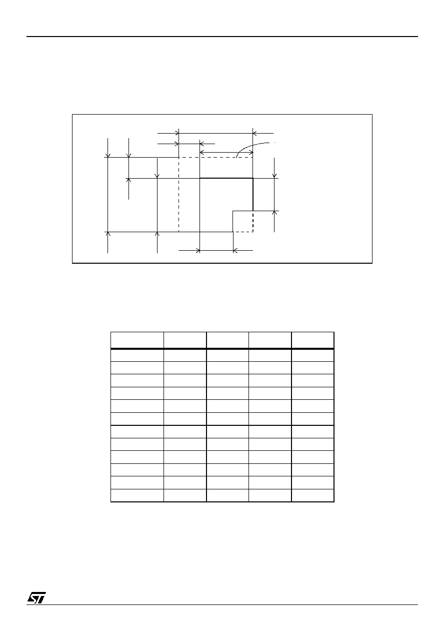
MECHANICAL SPECIFICATION
3
MECHANICAL SPECIFICATION
3.1
Alignment marks specification
3.2
Pads specification
The reference is the centre of the die (x=0, y=0)
Figure 3: Alignement marks
Table 1: Top side from left to right
Name
Centre: X
Centre: Y
Size: x
SIze: y
OUT54
-773.67
2796.11
76.00
92.00
OUT53
-670.48
2796.11
76.00
92.00
OUT52
-567.29
2796.11
76.00
92.00
OUT51
-464.1
2796.11
76.00
92.00
OUT50
-360.91
2796.11
76.00
92.00
OUT49
-257.72
2796.11
76.00
92.00
OUT48
-154.53
2796.11
76.00
92.00
OUT47
-51.34
2796.11
76.00
92.00
OUT46
51.85
2796.11
76.00
92.00
OUT45
155.04
2796.11
76.00
92.00
OUT44
258.23
2796.11
76.00
92.00
OUT43
361.42
2796.11
76.00
92.00
0.15
0.1
5
0.
2
5
m
i
n
.
0.
35
min. 0.35
min 0.1
mi
n 0
.
1
0.25
Patterning restricted area