STV7778S
DEFLECTION PROCESSOR FOR MULTISYNC MONITOR
September 1998
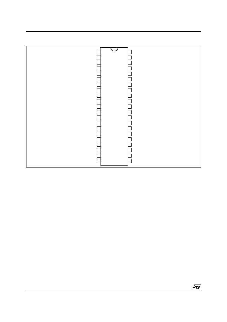
SHRINK42
(Plastic Package)
ORDER CODE : STV7778S
HORIZONTAL
.
DUAL PLL CONCEPT
.
SELF-ADAPTIVE (30 TO 70kHz)
.
X-RAY PROTECTION INPUT
.
DC ADJUSTABLE DUTY-CYCLE
.
INTERNAL 1st PLL LOCK/UNLOCK IDENTIFI-
CATION
.
WIDE RANGE DC CONTROLLED H-POSITION
.
ON/OFF SWITCH (FOR PWR MANAGEMENT)
.
TWO H-DRIVE POLARITIES
VERTICAL
.
VERTICAL RAMP GENERATOR
.
45 TO 120Hz AGC LOOP
.
DC CONTROLLED V-AMP, V-POS, S-AMP
AND S-CENTERING
.
ON/OFF SWITCH
B+ REGULATOR
.
INTERNAL PWM GENERATOR FOR B+
CURRENT MODE STEP-UP CONVERTER
.
DC ADJUSTABLE B+ VOLTAGE
.
OUTPUT PULSES SYNCHRONISED ON
HORIZONTAL FREQUENCY
.
INTERNAL MAX CURRENT LIMITATION
EWPCC
.
VERTICAL PARABOLA GENERATOR WITH DC
CONTROLLED KEYSTONE AND AMPLITUDE
GENERAL
.
COMPARED WITH THE STV7778, THE
STV7778S HAS AN INTERNAL METAL SHIELD
PROTECTION AGAINST OVERVOLTAGE.
.
POS/NEG H AND V SYNC POL
.
SEPARATED H AND V TTL INPUT
.
SAFETY BLANKING OUTPUT
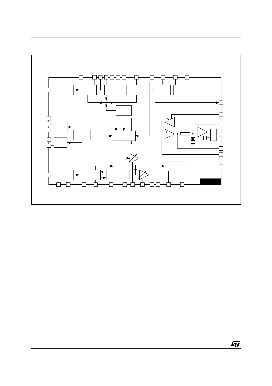
DESCRIPTION
The STV7778S is a monolithic integrated circuit
assembled in a 42 pins shrunk dual in line plastic
package.
The goal of this IC is to control all the functions
related to the horizontal and vertical deflection in a
multimodes or multisync monitor.
As can be seen in the block diagram, the
STV7778S includes the following functions :
- Positive or Negative sync polarities,
- Auto-sync horizontal processing,
- H-PLL lock/unlock identification,
- Auto-sync Vertical processing,
- East/West signal processing block,
- B+ controller,
- Safety blanking output.
An internal metal shield give to the STV7778S more
immunity against electromagnetic and electrostatic
fields, and therefore, additional safety for critical
applications (for example, in case of CRTs with
small coated area).
1/11

PIN-OUT DESCRIPTION
Pin N∞
Name
Function
1
PLL2C
Second PLL Loop Filter
2
H-DUTY
DC Control of Horizontal Drive Output Pulse Duty-cycle.
If this pin is grounded, the horizontal and vertical outputs are inhibited. By connecting a capacitor
on this pin a soft-start function may be realized on h-drive output.
3
H-FLY
Horizontal Flyback Input (Positive Polarity)
4
H-GND
Horizontal Section Ground. Must be connected only to components related to H blocks.
5
H-REF
Horizontal Section Reference Voltage. Must be filtered by capacitor to Pin 4
6
NC
7
NC
8
NC
9
NC
10
C0
Horizontal Oscillator Capacitor. To be connected to Pin 4.
11
R0
Horizontal Oscillator Resistor. To be connected to Pin 4.
12
PLL1F
First PLL Loop Filter. To be connected to Pin 4.
13
HLOCK-CAP
First PLL Lock/Unlock Time Constant Capacitor. Capacitor filtering the frequency change detected
on Pin13. When frequency is changing, a blanking pulse is generated on Pin 23, the duration of this
pulse is proportionnal to the capacitor on Pin 13. To be connected to Pin 4.
14
FH-MIN
DC Control for Free Running Frequency Setting. Comming from DAC output or DC voltage
generated by a resistor bridge connected between Pin 5 and 4.
15
H-POS
DC Control for Horizontal Centering
16
XRAY-IN
X-RAY Protection Input (with internal latch function)
17
H-SYNC
TTL Horizontal Sync Input
18
V
CC
Supply Voltage (12V Typical)
19
GND
Ground
20
H-OUTEM
Horizontal Drive Output (emiter of internal transistor)
21
H-OUTCOL
Horizontal Drive Output (open collector of internal transistor)
22
B+ OUT
B+ PWM Regulator Output
23
SBLK OUT
Safety Blanking Output. Activated during frequency changes, when X-RAY input is triggered or
when VS is too low.
24
VGND
Vertical Section Signal Ground
25
VAGCCAP
Memory Capacitor for Automatic Gain Control Loop in Vertical Ramp Generator
26
V
REF
Vertical Section Reference Voltage
27
VCAP
Vertical Sawtooth Generator Capacitor
28
VS-AMP
DC Control of Vertical S Shape Amplitude
29
VS-CENT
DC Control of Vertical S Centering
30
VOUT
Vertical Ramp Output (with frequency independant amplitude and S-correction)
31
V-AMP
DC Control of Vertical Amplitude Adjustment
32
V
DCOUT
Vertical Position Reference Voltage Output Temperature Matched with V-AMP Output
33
V-POS
DC Control of Vertical Position Adjustment
34
VSYNC
Vertical TTL Sync Input
35
PLL1INHIB
TTL Input for PLL1 Output Current Inhibition (To be used in case of comp sync input signal)
36
E/WOUT
East/West Pincushion Correction Parabola Output
37
E/W-AMP
DC Control of East/West Pincushion Correction Amplitude
38
KEYST
DC Control of Keystone Correction
39
B+ ADJ
DC Control of B+ Adjustment
40
REGIN
Regulation Input of B+ Control Loop
41
COMP
B+ Error Amplifier Output for Frequency Compensation and Gain Setting
42
I
SENSE
Sensing of External B+ Switching Transistor Emiter Current
77
78
S
-
0
1
.
T
B
L
STV7778S
3/11
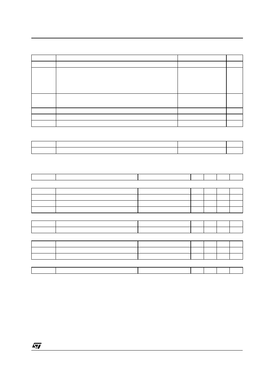
HORIZONTAL SECTION
Operating conditions
Symbol
Parameter
Test conditions
Min.
Typ.
Max.
Unit
VCO
R0min
Oscillator Resistor Min Value
Pin 11
6
k
C0min
Oscillator Capacitor Min Value
Pin 10
390
pF
Fmax
Maximum Oscillator Frequency
70
kHz
HsVR
Horizontal Sync Input Voltage
Pin 17
0
5.5
V
INPUT SECTION
MinD
Minimum Input Pulses Duration
Pin 17
1
µ
S
Mduty
Maximum Input Signal Duty Cycle
Pin 17
25
%
OUTPUT SECTION
I3m
Maximum Input Peak Current on Pin 3
2
mA
HOI1
Horizontal Drive Output Max Current
Pin 20, sourced current
20
mA
HOI2
Horizontal Drive Output Max Current
Pin 21, sunk current
20
mA
DC CONTROL VOLTAGES
DCadj
DC Voltage Range on DC Controls
V
REF-H
= 8V, Pins 2-14-15
2
6
V
77
78S
-
0
4
.
T
B
L
ABSOLUTE MAX RATING
Symbol
Parameter
Value
Unit
V
CC
Supply Voltage (Pin 18)
13.5
V
V
IN
Max Voltage on
Pins 2, 14, 15, 28, 29, 31, 33, 37, 38, 39
Pin 3
Pins 17, 34
Pin 40
Pin 42
Pin 16
8
1.8
6
8
8
6
V
VESD
ESD Succeptibility
Human Body Model, 100pF Discharge through 1.5k
EIAJ Norm, 200pF Discharge through 0
2
300
kV
V
T
stg
Storage Temperature
-40, +150
∞C
T
j
Max Operating Junction Temperature
150
∞C
T
oper
Operating Temperature
0, +70
∞C
77
78
S
-
0
2.
T
B
L
THERMAL DATA
Symbol
Parameter
Value
Unit
R
th (j-a)
Junction-Ambient Thermal Resistance
Max.
65
∞C/W
77
78
S
-
0
3.
T
B
L
STV7778S
5/11