 | –≠–ª–µ–∫—Ç—Ä–æ–Ω–Ω—ã–π –∫–æ–º–ø–æ–Ω–µ–Ω—Ç: STV7801SP | –°–∫–∞—á–∞—Ç—å:  PDF PDF  ZIP ZIP |
This is preliminary information on a new product in development or undergoing evaluation. Details are subject to change without notice.
Revision 3.3
June 2000
1/18
STV7801S
PLASMA DATA POWER SWITCH
PRELIMINARY DATA
FEATURES
s
High Voltage - Low Power Pulse Generator
s
100V Absolute Maximum Supply
s
High Load Drive Capability (25nF)
s
5V Compatible Input Logic
s
Very Low Stand-by Current
s
Power Recovery High Current (±7A)
s
Totem Pole High Output Current (±5A)
s
Built-in Timing Control & Thermal Protection
s
BCD Technology
s
Packaging: Multiwatt 15, Power SO20
DESCRIPTION
STV7801 is a monolithic integrated circuit imple-
mented in STMicroelectronics BCD proprietary
technology designed as a switched power supply
generator for data drivers in a Plasma Display
Panel (P.D.P.) application.
The high load drive capability of the STV7801 re-
duces the number of devices necessary to drive a
complete PDP (4 to 6 devices for a 42" VGA 16/9
PDP monitor).
The STV7801 high current drive capability pro-
vides a high power recovery efficiency coefficient
superior to 85% on constant capacitive load.
To limit the number of external components, the
device integrates level shifters driven with 5V
CMOS compatible levels.
To increase the reliability of the system, the device
integrates several protections such as output
over-voltage, over-temperature, power-ON pro-
tection.
.
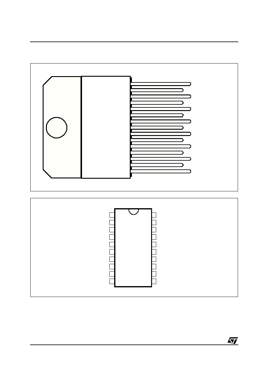
MULTIWATT 15 (Plastic Package)
ORDER CODE: STV7801S
20 leads
POWERSO20 (Plastic Package)
ORDER CODE: STV7801SP
Customer samples will be available
by september 2000
1
STV7801S
2/18
1 - PIN CONNECTION
Multiwatt 15
PowerSO20
1
2
3
4
5
6
7
8
9
10
11
12
13
14
15
Vpp
Vpp
CBoot
Out
Vssp
Vdd
DM-LH
Vsslog
PR
DM-HL
PR-FPS
LH-Tr
L-Clmp
H-Clmp
HL-Tr
1
2
3
4
5
6
7
8
9
10
11
12
13
14
15
16
17
18
19
20
Vsssub
HL-Tr
H-Clmp
L-Clmp
PR-FPS
PR-FPS
DM-HL
PR
Vsssub
Vsssub
Vpp
Vpp
CBoot
Out
Vssp
Vdd
DM-LH
Vsslog
Vssp
LH-Tr
2
STV7801S
3/18
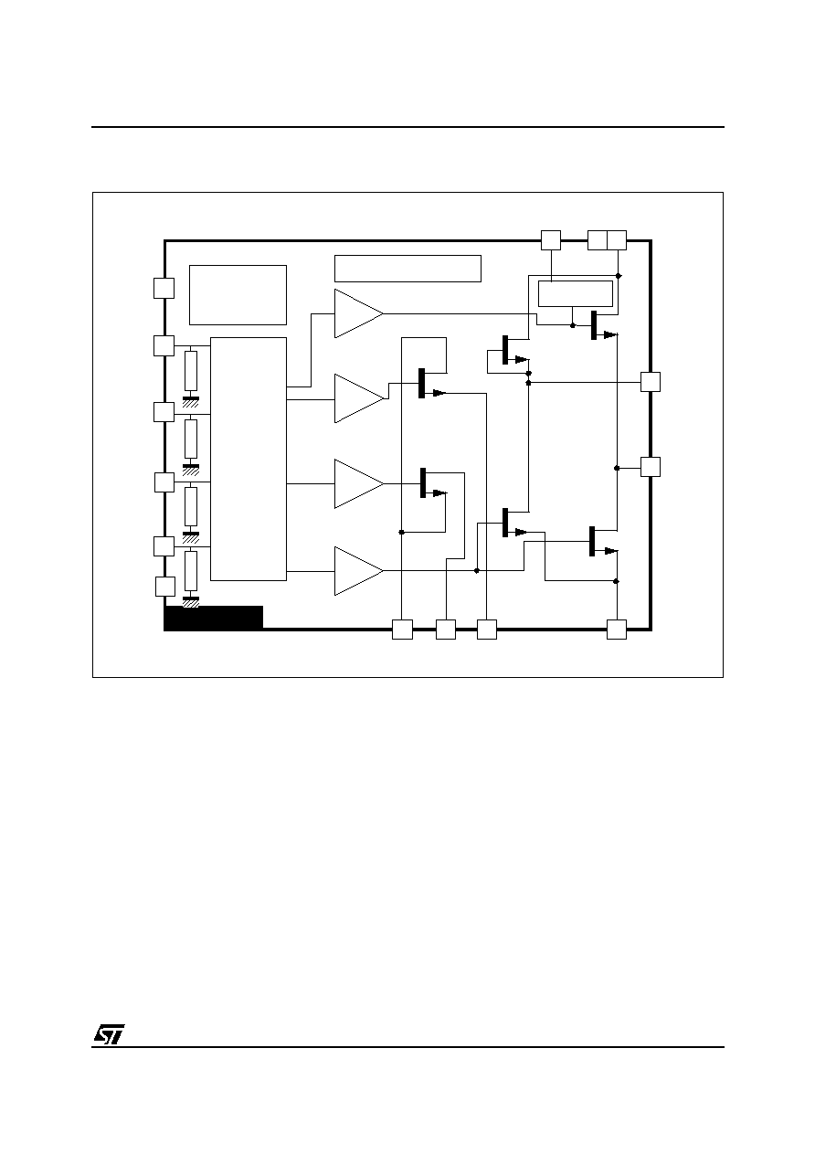
2 - BLOC DIAGRAM
MULTIWATT 15
10
3
1
4
2
8
13
15 14
7
12
11
9
6
5
CBoot
Vpp
Out
Vssp
Vdd
DM-LH
Vsslog
PR
DM-HL
PR-FPS
LH-Tr
L-Clmp
H-Clmp
HL-Tr
STV7801S
Protection
Control
Timing
Control
Voltage Control
Transistor
H-Clmp
Transistor
L-Clmp
LH Transistor
HL Transistor
Bootstrap
control
STV7801S
4/18
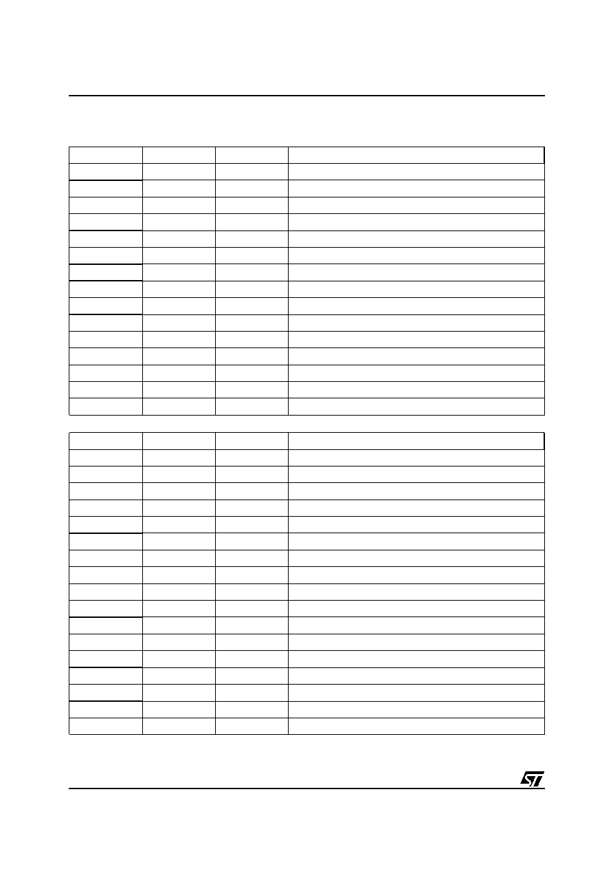
3 - PIN DESCRIPTION
Multiwatt 15
PowerSO20
Pin Number
Pin Name
Function
Description
1
HL-Tr
Input
Power Recovery High Level/Low Level Transition
2
H-Clmp
Input
Main Switch High-Side Clamp Input
3
L-Clmp
Input
Main Switch Low-Side Clamp Input
4
LH-Tr
Input
Power Recovery Low Level/High Level Transition
5
PR-FPS
Input
Power Recovery Floating Supply
6
DM-HL
Input
Current Recirculation- Input Pin - High/Low Transition
7
PR
Output
Power Recirculation Output Stage
8
Vsslog
Ground
Logic Ground/Substrate Ground
9
DM-LH
Output
Current Recirculation- Output Pin - Low/High Transition
10
Vdd
Supply
Logic Supply
11
Vssp
Ground
Power Ground
12
Out
Output
Main Switch Output
13
CBoot
Input
Bootstrap Capacitor Input Pin
14
Vpp
Supply
High Voltage Supply
15
Vpp
Supply
High Voltage Supply
Pin Number
Pin Name
Function
Description
1
Vssub
Ground
Substrate Ground
2
HL-Tr
Input
Power Recovery High Level/Low Level Transition
3
H-Clmp
Input
Main Switch High-Side Clamp Input
4
L-Clmp
Input
Main Switch Low-Side Clamp Input
5
LH-Tr
Input
Power Recovery Low Level/High Level Transition
6
PR-FPS
Input
Power Recovery Floating Supply
7
PR-FPS
Input
Power Recovery Floating Supply
8
DM-HL
Input
Current Recirculation- Input Pin - High/Low Transition
9
PR
Output
Power Recirculation Output Stage
10
Vssub
Ground
Substrate Ground
11
Vsslog
Ground
Logic Ground/Substrate Ground
12
DM-LH
Output
Current Recirculation- Output Pin - Low/High Transition
13
Vdd
Supply
Logic Supply
14
Vssp
Ground
Power Ground
15
Vssp
Ground
Power Ground
16
Out
Output
Main Switch Output
17
CBoot
Input
Bootstrap Capacitor Input Pin
STV7801S
5/18
4 - CIRCUIT DESCRIPTION
STV7801 is a monolithic integrated circuit imple-
mented in ST Microelectronics BCD proprietary
technology designed as a switched power supply
generator for data drivers in a Plasma Display
Panel (P.D.P.) application.
The high load drive capability of STV7801 reduces
the number of devices necessary to drive a com-
plete PDP (4 to 6 devices for a 42" VGA 16/9 PDP
monitor).
STV7801 high current drive capability provides a
high power recovery efficiency coefficient superior
to 85% on constant capacitive load. The structure
of the output stage is implemented with 2 DMOS
transistors to minimise the die size. External com-
ponents like bootstrap capacitor can also be im-
plemented to increase the performances of the cir-
cuit.
STV7801 integrates level shifters driven with 5V
CMOS compatible levels. This feature reduces the
number of discrete components such as voltage
translators.
STV7801 integrates several protections like output
over-voltage, timing control and over-temperature
to increase the reliability of the system.
Over-voltage protection consists in clamping di-
odes connected between Vpp, Vssp and critical
nodes of the devices.
Timing control consists in a monitoring of the out-
put stage control signals to avoid any cross-con-
duction.
Over-temperature protection is activated when
junction temperature reaches the threshold values
fixed internally and sets the device in tri-state
mode.
STV7801 can drive several data drivers connected
to column electrodes of the panel. The maximum
amount of data drivers is given by the Power Re-
covery Current of the device and then the maxi-
mum rise/fall time of the signal. The rise and fall
time of the AC supply signal is adjusted by the val-
ue of the inductance connected to the panel ca-
pacitance through the data drivers. The amount of
STV7801 needed to generate the AC supply can
be reduced by increasing the rise/fall time of the
generated AC supply.
5 - CONTROL SIGNALS TRUTH TABLE
18
Vpp
Supply
High Voltage Supply
19
Vpp
Supply
High Voltage Supply
20
Vssub
Ground
Substrate Ground
Pin Number
Pin Name
Function
Description
HL-Tr
LH-Tr
L-Clmp
H-Clmp
Device Output
Comments
L
H
L
L
Low to High Transition
Power Saving Mode
H
L
L
L
High to Low Transition
Power Saving Mode
L
X
L
H
Vpp
Power Supply Clamp
X
L
H
L
Vssp
Power Ground Clamp
X
X
H
H
Tri-State
Protection Mode
X
H
H
X
Tri-State
Protection Mode
H
X
X
H
Tri-State
Protection Mode
L
L
L
L
Tri-State
Protection Mode