STV80NE03L-06
N - CHANNEL 30V - 0.005
- 80A - PowerSO-10
STripFET
TM
MOSFET
s
TYPICAL R
DS(on)
= 0.005
s
EXCEPTIONAL dv/dt CAPABILITY
s
100% AVALANCHE TESTED
s
LOW GATE CHARGE 100
o
C
s
APPLICATION ORIENTED
CHARACTERIZATION
DESCRIPTION
This Power Mosfet is the latest development of
STMicroelectronics
unique
"Single
Feature
Size
TM
"
strip-based
process.
The
resulting
transistor shows extremely high packing density
for
low
on-resistance,
rugged
avalance
characteristics and less critical alignment steps
therefore
a
remarkable
manufacturing
reproducibility.
APPLICATIONS
s
HIGH CURRENT, HIGH SPEED SWITCHING
s
SOLENOID AND RELAY DRIVERS
s
MOTOR CONTROL, AUDIO AMPLIFIERS
s
DC-DC & DC-AC CONVERTERS
s
AUTOMOTIVE ENVIRONMENT (INJECTION,
ABS, AIR-BAG, LAMPDRIVERS, Etc. )
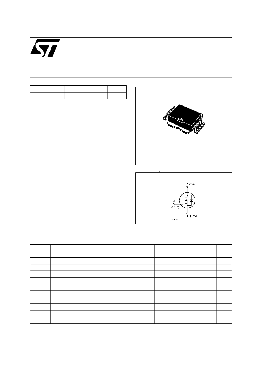
INTERNAL SCHEMATIC DIAGRAM
May 2000
1
10
PowerSO-10
ABSOLUTE MAXIMUM RATINGS
Symbol
Parameter
Value
Un it
V
DS
Drain-source Voltage (V
GS
= 0)
30
V
V
DGR
Drain- gate Voltage (R
GS
= 20 k
)
30
V
V
GS
G ate-source Volt age
±
20
V
I
D
Drain Current (continuous) at T
c
= 25
o
C
80
A
I
D
Drain Current (continuous) at T
c
= 100
o
C
60
A
I
DM
(
∑
)
Drain Current (pulsed)
320
A
P
tot
T otal Dissipat ion at T
c
= 25
o
C
150
W
Derating Factor
1
W /
o
C
dv/dt
Peak Diode Recovery voltage slope
7
V/ns
T
s tg
Storage Temperature
-65 to 175
o
C
T
j
Max. Operating Junction Temperature
175
o
C
(
∑
) Pulse width limited by safe operating area
(
1
) I
SD
80 A, di/dt
300 A/
µ
s, V
DD
V
(BR)DSS
, T
j
T
JMAX
T YPE
V
DSS
R
DS(on)
I
D
STV80NE03L-06
30 V
< 0. 006
80 A
1/8
THERMAL DATA
R
thj -case
Rthj -amb
R
thc-sink
T
l
Thermal Resistance Junction-case
Max
Thermal Resistance Junction-ambient
Max
Thermal Resistance Case-sink
Typ
Maximum Lead Temperature F or Soldering Purpose
1
62.5
0.5
300
o
C/W
oC/ W
o
C/W
o
C
AVALANCHE CHARACTERISTICS
Symbo l
Parameter
Max Value
Unit
I
AR
Avalanche Current, Repetitive or Not-Repetitive
(pulse width limited by T
j
max,
< 1%)
80
A
E
AS
Single Pulse Avalanche Energy
(starting T
j
= 25
o
C, I
D
= I
AR
, V
DD
= 15 V)
600
mJ
ELECTRICAL CHARACTERISTICS (T
J =
- 40 to 150
o
C unless otherwise specified)
OFF
Symbo l
Parameter
Test Con ditions
Min.
Typ.
Max.
Unit
V
(BR)DSS
Drain-source
Breakdown Voltage
I
D
= 250
µ
A
V
GS
= 0
I
D
= 250
µ
A
V
GS
= 0
T
c
=25
o
C
27
30
V
I
DSS
Zero Gat e Voltage
Drain Current (V
GS
= 0)
V
DS
= Max Rat ing
T
c
=25
o
C
V
DS
= Max Rat ing
1
50
µ
A
µ
A
I
G SS
Gat e-body Leakage
Current (V
DS
= 0)
V
GS
=
±
20 V
±
100
nA
ON (
)
Symbo l
Parameter
Test Con ditions
Min.
Typ.
Max.
Unit
V
G S(th)
Gat e Threshold Voltage V
DS
= V
GS
I
D
= 250
µ
A
V
DS
= V
GS
I
D
= 250
µ
A
T
J
=25
o
C
0. 6
1.7
3. 0
2. 5
V
R
DS(on)
Static Drain-source On
Resistance
V
GS
= 10V
I
D
= 40 A
V
GS
= 5V
I
D
= 40 A
V
GS
= 10V
I
D
= 40 A
T
J
=25
o
C
V
GS
= 5V
I
D
= 40 A
T
J
=25
o
C
0.005
0.012
0.018
0.006
0.009
I
D(o n)
On State Drain Current
V
DS
> I
D(o n)
x R
DS(on )ma x
V
GS
= 10 V
40
A
DYNAMIC
Symbo l
Parameter
Test Con ditions
Min.
Typ.
Max.
Unit
g
f s
(
)
Forward
Transconductance
V
DS
> I
D(o n)
x R
DS(on )ma x
I
D
=40 A
20
S
C
iss
C
os s
C
rss
Input Capacitance
Out put Capacitance
Reverse Transfer
Capacitance
V
DS
= 25 V
f = 1 MHz
V
GS
= 0
6500
1500
500
8700
2000
700
pF
pF
pF
STV80NE03L-06
2/8
ELECTRICAL CHARACTERISTICS (continued)
SWITCHING ON
Symbo l
Parameter
Test Con ditions
Min.
Typ.
Max.
Unit
t
d(on)
t
r
Turn-on Time
Rise Time
V
DD
= 15 V
I
D
= 40 A
R
G
=4.7
V
GS
= 5 V
(see t est circuit, f igure 3)
40
260
55
350
ns
ns
Q
g
Q
gs
Q
gd
Tot al G ate Charge
Gat e-Source Charge
Gat e-Drain Charge
V
DD
= 24 V
I
D
= 80 A
V
G S
= 5 V
95
30
44
130
nC
nC
nC
SWITCHING OFF
Symbo l
Parameter
Test Con ditions
Min.
Typ.
Max.
Unit
t
r (Voff)
t
f
t
c
Off -volt age Rise T ime
Fall T ime
Cross-over Time
V
DD
= 24 V
I
D
= 80 A
R
G
=4.7
V
GS
= 5 V
(see t est circuit, f igure 5)
70
165
250
95
220
340
ns
ns
ns
SOURCE DRAIN DIODE
Symbo l
Parameter
Test Con ditions
Min.
Typ.
Max.
Unit
I
SD
I
SDM
(
∑
)
Source-drain Current
Source-drain Current
(pulsed)
80
320
A
A
V
SD
(
)
Forward On Voltage
I
SD
= 80 A
V
GS
= 0
1. 5
V
t
rr
Q
rr
I
RRM
Reverse Recovery
Time
Reverse Recovery
Charge
Reverse Recovery
Current
I
SD
= 80 A
di/ dt = 100 A/
µ
s
V
DD
= 15 V
T
j
= 150
o
C
(see t est circuit, f igure 5)
75
0.14
4
ns
µ
C
A
(
) Pulsed: Pulse duration = 300
µ
s, duty cycle 1.5 %
(
∑
) Pulse width limited by safe operating area
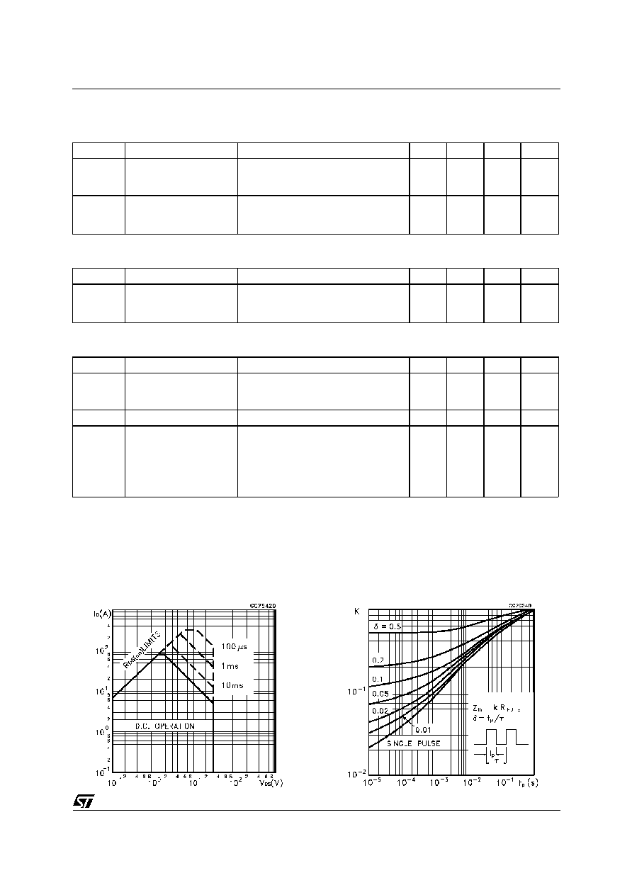
Safe Operating Area for
Thermal Impedance
STV80NE03L-06
3/8
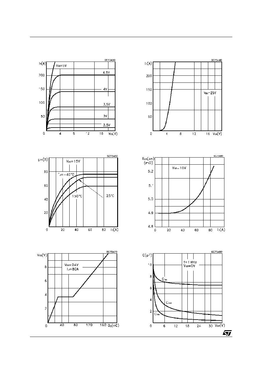
Output Characteristics
Transconductance
Gate Charge vs Gate-source Voltage
Transfer Characteristics
Static Drain-source On Resistance
Capacitance Variations
STV80NE03L-06
4/8
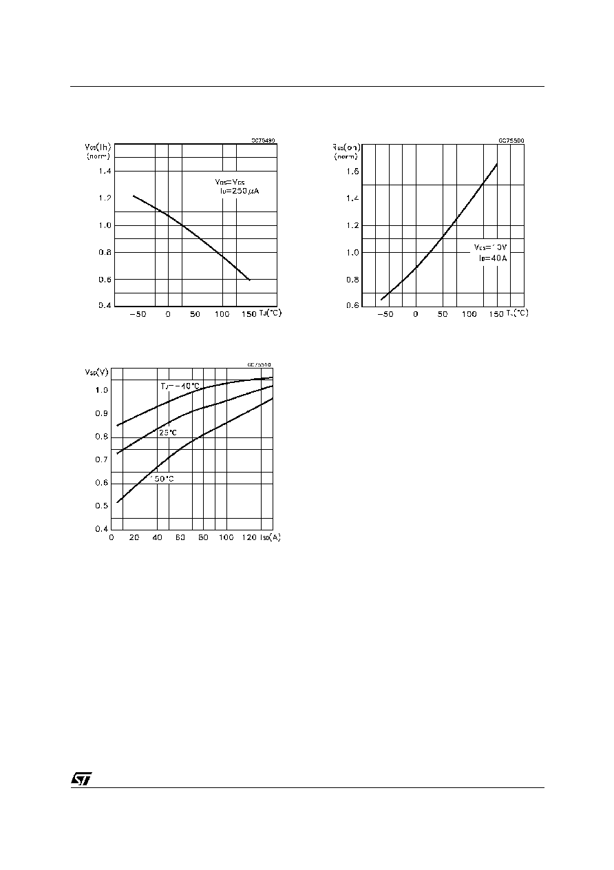
Normalized Gate Threshold Voltage vs
Temperature
Source-drain Diode Forward Characteristics
Normalized On Resistance vs Temperature
STV80NE03L-06
5/8