 | –≠–ª–µ–∫—Ç—Ä–æ–Ω–Ω—ã–π –∫–æ–º–ø–æ–Ω–µ–Ω—Ç: STV8130AD | –°–∫–∞—á–∞—Ç—å:  PDF PDF  ZIP ZIP |
PRELIMINARY DATA
STV8130AD
ADJUSTABLE AND +3.3 V DUAL VOLTAGE REGULATOR
WITH DISABLE AND RESET FUNCTIONS
Æ
This is preliminary information on a new product now in development or undergoing evaluation. Details are subject to change without notice.
September 2003
1/12
FEATURES
s
Input Voltage Range: 5 V to 18 V
s
Output Currents up to 750 mA
s
Fixed Precision Output 1 Voltage: 3.3 V ±2%
s
Adjustable Output 2 Voltage: 2.8 to 16 V
s
Output 1 with Reset Function
s
Output 2 with Disable Function by TTL Input
s
Short-circuit Protection at both Outputs
s
Thermal Protection
s
Low Dropout Voltage
DESCRIPTION
The STV8130A# and STV8130D# are monolithic
dual positive voltage regulators designed to provide
a fixed precision output voltage of 3.3 V and an
adjustable voltage between 2.8 and 16 V for
currents up to 750 mA.
An internal reset circuit generates a reset pulse
when the voltage of Output 1 drops below the
regulated voltage value.
Output 2 can be disabled via the TTL input.
Short-circuit and thermal protections are included.
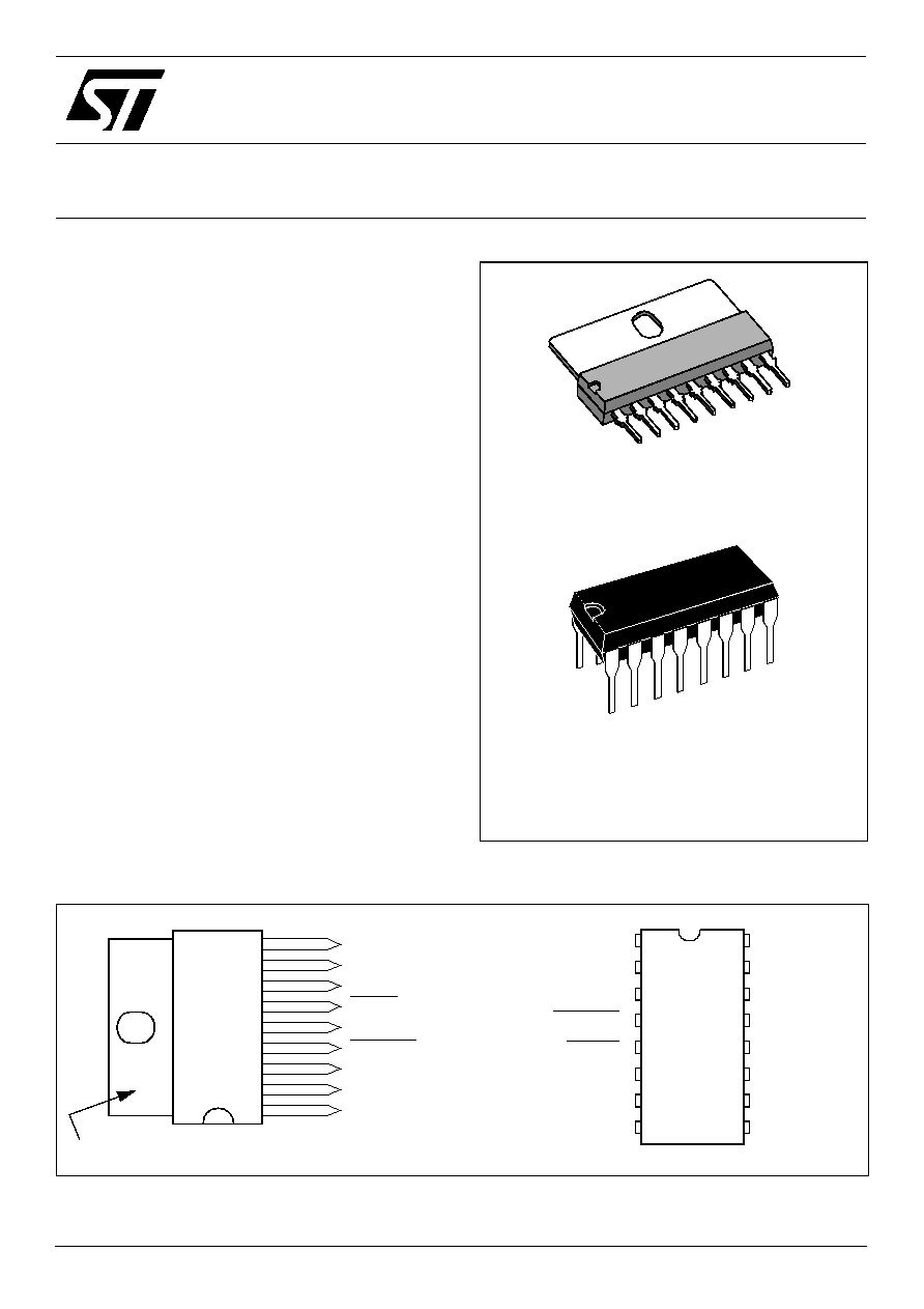
SIP9 (Plastic Package)
ORDER CODE: STV8130A#
DIP16 (8 + 8)
ORDER CODE: STV8130D#
9
8
7
6
5
4
3
2
1
OUTPUT1
OUTPUT2
PROGRAM
RESET
GROUND
DISABLE
DELAY CAPACITOR
INPUT2
INPUT1
Tab is connected to GROUND
1
2
3
4
5
6
7
8
11
12
13
14
15
16
INPUT1
INPUT2
DELAY CAPACITOR
DISABLE
RESET
PROGRAM
OUTPUT2
OUTPUT1
GROUND
GROUND
GROUND
GROUND
GROUND
GROUND
GROUND
GROUND
10
9

STV8130AD
2/12
TABLE OF CONTENTS
Chapter 1
GENERAL INFORMATION . . . . . . . . . . . . . . . . . . . . . . . . . . . . . . . . . . . . . . . . . .3
Chapter 2
ELECTRICAL CHARACTERISTICS . . . . . . . . . . . . . . . . . . . . . . . . . . . . . . . . . . . .4
2.1
Absolute Maximum Ratings ................................................................................................ 4
2.2
Thermal Data ...................................................................................................................... 4
2.3
Electrical Characteristics ...................................................................................................... 4
Chapter 3
CIRCUIT DESCRIPTION . . . . . . . . . . . . . . . . . . . . . . . . . . . . . . . . . . . . . . . . . . . . .6
Chapter 4
APPLICATION DIAGRAMS . . . . . . . . . . . . . . . . . . . . . . . . . . . . . . . . . . . . . . . . .7
Chapter 5
POWER DISSIPATION AND LAYOUT INDICATIONS . . . . . . . . . . . . . . . . . . . . . .8
Chapter 6
PACKAGE MECHANICAL DATA . . . . . . . . . . . . . . . . . . . . . . . . . . . . . . . . . . . .9
Chapter 7
REVISION HISTORY . . . . . . . . . . . . . . . . . . . . . . . . . . . . . . . . . . . . . . . . . . . . . . .11
3/12
STV8130AD
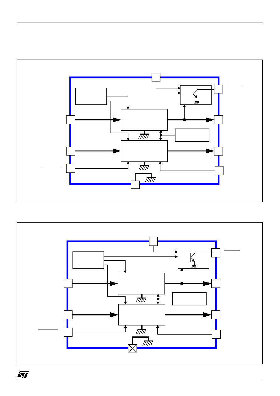
GENERAL INFORMATION
1
GENERAL INFORMATION
Figure 1: STV8130A
#
Block Diagram
Figure 2: STV8130D
#
Block Diagram
1
Regulator 1
2
8
Regulator 2
6
9
Reference
7
4
INPUT1
INPUT2
DISABLE
OUTPUT1
OUTPUT2
RESET
DELAY CAPACITOR
PROGRAM
GROUND
5
3
Protection
1
Regulator 1
2
7
Regulator 2
5
8
Reference
6
4
INPUT1
INPUT2
DISABLE
OUTPUT1
OUTPUT2
RESET
DELAY CAPACITOR
PROGRAM
GROUND
3
Protection
Pins 9 to 16
ELECTRICAL CHARACTERISTICS
STV8130AD
4/12
2
ELECTRICAL CHARACTERISTICS
2.1
Absolute Maximum Ratings
2.2
Thermal Data
2.3
Electrical Characteristics
T
AMB
= 25∞ C, V
IN1
= 7 V, V
IN2
= 10 V, unless otherwise specified.
Symbol
Parameter
Value
Unit
V
IN
DC Input Voltage at pins INPUT1 and INPUT2
20
V
V
DIS
Disable Input Voltage at pin DISABLE
20
V
V
RST
Output Voltage at pin RESET
20
V
I
OUT1,2
Output Currents
Internally Limited
P
t
Power Dissipation
Internally Limited
T
STG
Storage Temperature
-65 to +150
∞C
T
J
Junction Temperature
0 to +150
∞C
Symbol
Parameter
Value
Unit
R
thJC
Thermal Resistance
(Junction-to-Case)
STV8130A
#
STV8130D
#
9
15
∞C/W
R
thJA
Thermal Resistance
1
(Junction-to-Ambient)
1. Mounted on board. For more information, refer to
Section 5
.
STV8130A
#
STV8130D
#
50
56
∞C/W
T
J
Maximum Recommended Junction Temperature
140
∞C
T
OPER
Operating Free Air Temperature Range
0 to +70
∞C
Symbol
Parameter
Test Conditions
Min.
Typ.
Max.
Unit
V
OUT1
Output Voltage
I
OUT1
= 10 mA
3.23
3.30
3.37
V
V
OUT2
Output Voltage
I
OUT2
= 10 mA
2.8
16.0
V
V
IO1,2
Dropout Voltage
I
OUT1,2
= 750 mA
1.4
V
V
O1,2LI
Line Regulation
6 V < V
IN1
< 12 V
12 V < V
IN2
< 18 V
I
OUT1,2
= 200 mA
50
100
mV
V
O1,2LO
Load Regulation
5 mA < I
OUT1
< 600 mA
5 mA < I
OUT2
< 600 mA
100
200
mV
5/12
STV8130AD
ELECTRICAL CHARACTERISTICS
I
Q
Quiescent Current
I
OUT1
= 10 mA, OUTPUT2
Disabled
2
mA
V
O1RST
Reset Threshold Voltage
1
K = V
OUT1
, I
OUT1
50 mA
K - 0.4
K - 0.25
K - 0.1
V
V
RTH
Reset Threshold Hysteresis
See circuit description.
20
50
75
mV
t
RD
Reset Pulse Delay
C
e
= 100 nF
See circuit description.
25
ms
V
RL
Saturation Voltage in Reset Condition I
RESET
= 5 mA
0.4
V
I
RH
Leakage Current in Normal Condition
V
RESET
= 10 V
10
µA
K
OUT1, 2
Output Voltage Thermal Drift
T
J
= 0 to + 125∞C
100
ppm/∞C
I
OUT1,2SC
Short Circuit Output Current
V
IN1
= 7 V, V
IN2
= 10 V
V
IN1,2
= 16 V
2
1.6
1.0
A
V
DISH
Disable Voltage when pin DISABLE is High (OUTPUT2 active)
2
V
V
DISL
Disable Voltage when pin DISABLE is Low (OUTPUT2 disabled)
0.8
V
I
DIS
Disable Bias Current
0 V < V
DIS
< 7 V
-100
2
µA
V
REF
Reference Voltage at PROGRAM Pin
2.44
V
T
JSD
Junction Temperature for Thermal Shutdown
145
∞C
1. This reset signal is activated by a decrease of V
OUT1
voltage which can be due to an overload of pin OUT1
or by a lack of Input Voltage (V
IN1
).
2. The output short-circuit currents are tested one channel at time. During a short-circuit, a large consumption
of power occurs, but the thermal protection circuit prevents any excessive temperatures. A safe permanent
short-circuit protection is only guaranteed for input voltages up to 16 V.
Symbol
Parameter
Test Conditions
Min.
Typ.
Max.
Unit
K
0
V
0
10
6
T V
0
------------------------
=