 | –≠–ª–µ–∫—Ç—Ä–æ–Ω–Ω—ã–π –∫–æ–º–ø–æ–Ω–µ–Ω—Ç: STV8131 | –°–∫–∞—á–∞—Ç—å:  PDF PDF  ZIP ZIP |
September 2003
1/5
This is preliminary information on a new product now in development. Details are subject to change without notice.
STV8131
5V AND 8V VOLTAGE REGULATOR
PRODUCT PREVIEW
FEATURES
s
Output Currents up to 1A
s
Fixed Precision Output 1 Voltage 5V ± 2%
s
Fixed Precision Output 2 Voltage 8V ± 2%
s
Output 1 with Disable by TTL Input
s
Output 2 with Disable by TTL Input
s
Short Circuit Protection at both Outputs
s
Thermal Protection
s
Low Drop Output Voltage
DESCRIPTION
The STV8131 is a monolithic dual positive voltage
regulator designed to provide fixed precision out-
put voltages of 5V and 8V at currents up to 1A.
Each output can be disabled separately by a TTL
input.
Short circuit and thermal protections are included.
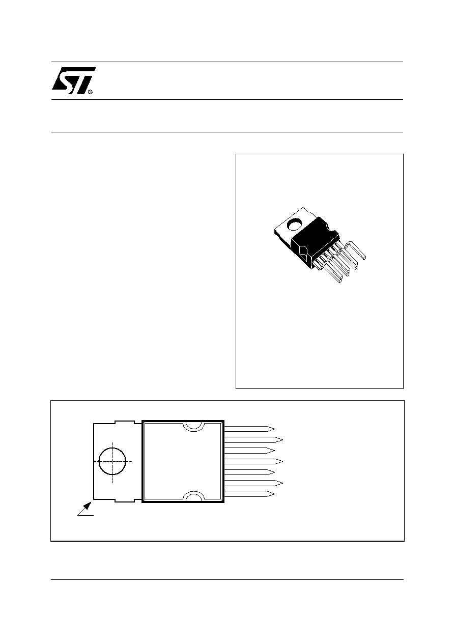
Figure 1. Pin Connections
HEPTAWATT
(Plastic Package)
ORDER CODES: STV8131
8131
-
01.e
p
s
7
6
5
4
3
2
1
Tab connected to Pin 4
OUTPUT 1
OUTPUT 2
INPUT 2
INPUT 1
GROUND
DISABLE FOR OUTPUT 2
DISABLE FOR OUTPUT 1
1
STV8131
2/5
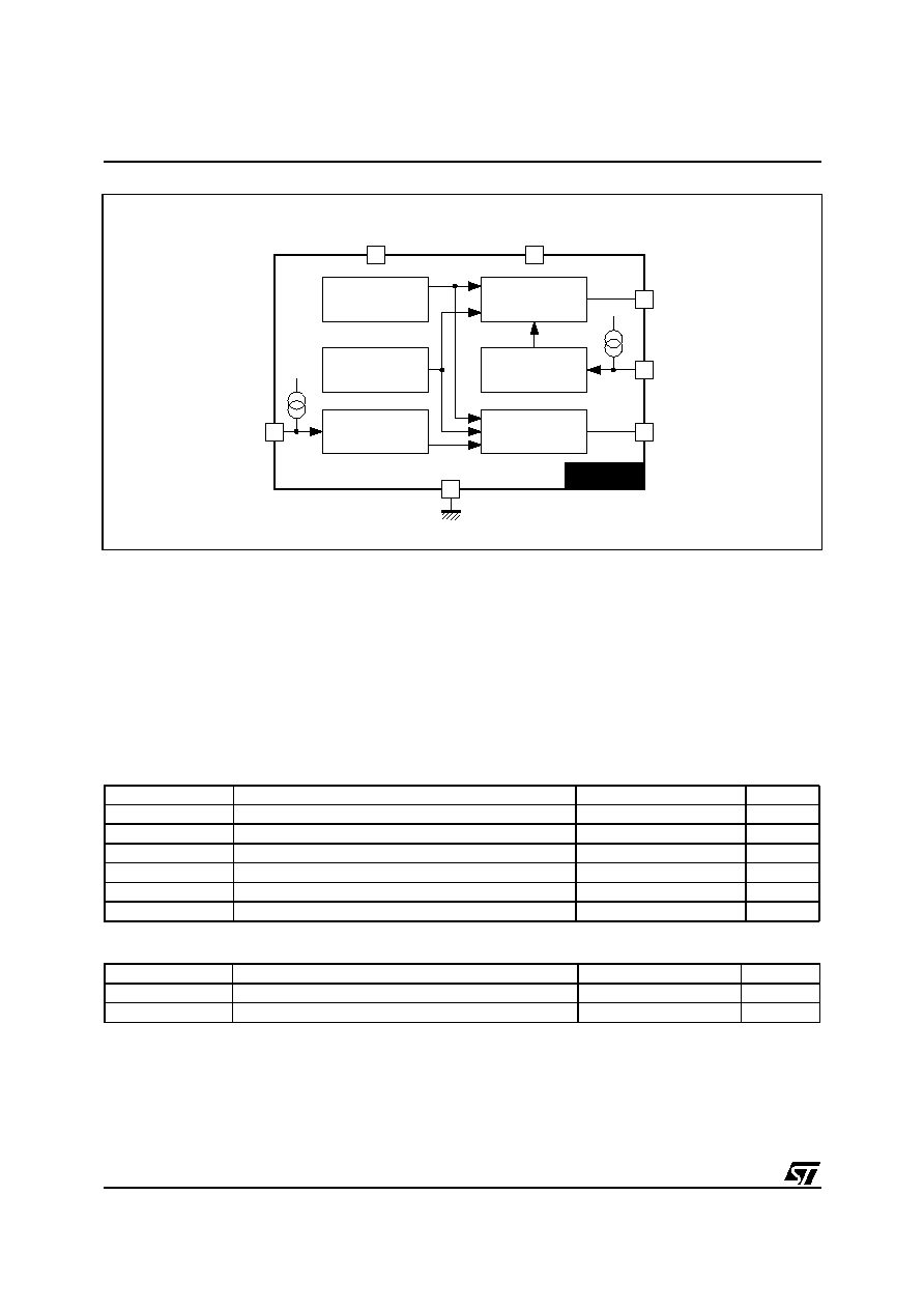
Figure 2. Block Diagram
CIRCUIT DESCRIPTION
The STV8131 is a dual voltage regulator with sep-
arate Disable for each output.
The two regulation parts are supplied from one
voltage reference circuit trimmed by zener zap
during EWS test.
Since the supply voltage of this last is connected
at Pin 1 (V
IN1
), the regulator 2 will not work if Pin 1
is not supplied.
The outputs stage have been realized in darlington
configuration with a drop typical 1.2V.
For each output a disable circuit switches-off this
output if a voltage lower than 0.8V is applied at
corresponding Pin (Pin 3 for output 2, Pin 5 for out-
put 1).
ABSOLUTE MAXIMUM RATINGS
THERMAL DATA
8131-
02.ep
s
1
2
3
4
5
6
7
REFERENCE
OUTPUT 1
OUTPUT 2
PROTECTION
DISABLE
DISABLE
STV8131
OUTPUT 2
OUTPUT 1
DISABLE
DISABLE
INPUT 1
INPUT 2
Symbol
Parameter
Value
Unit
V
IN
DC Input Voltage Pin 1
20
V
V
DIS
Disable Input Voltage Pin 3-5
20
V
I
O1, 2
Output Currents
Internally Limited
P
t
Power Dissipation
Internally Limited
T
STG
Storage Temperature
- 65 to + 150
∞C
T
J
unction Temperature
0 to + 150
∞C
Symbol
Parameter
Value
Unit
R
TH
(j-c)
Thermal Resistance Junction-case
Max.
3
∞C/W
T
J
Recommended Junction Temperature
Max.
130
∞C
1
STV8131
3/5
ELECTRICAL CHARACTERISTICS
(V
IN1
= 7V, V
IN2
= 10V, T
J
= 25∞C unless otherwise specified)
Note: Safe permanent short-circuit is only guaranteed for input voltages up to 16V.
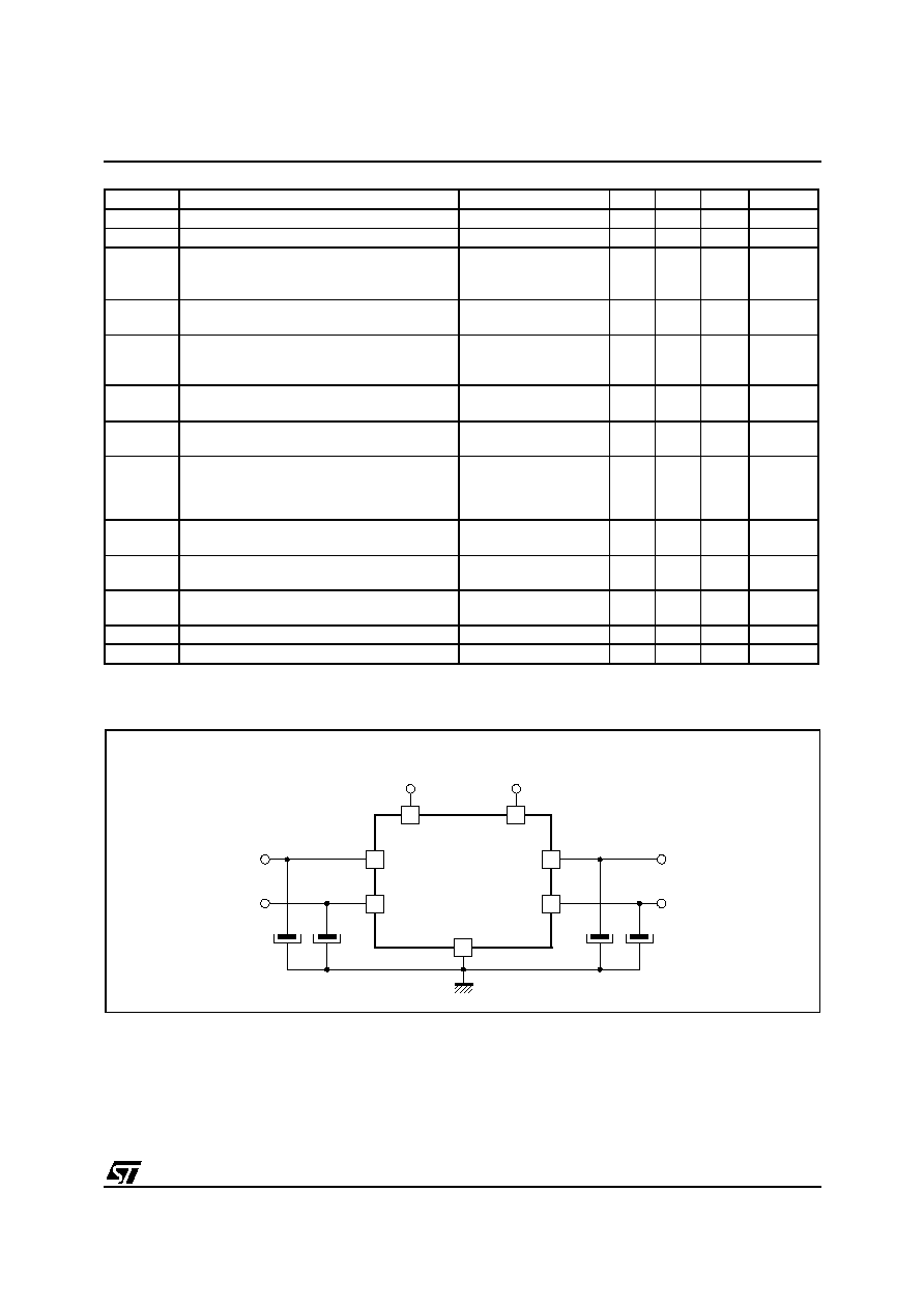
Figure 3. Typical Application
Symbol
Parameter
Test Conditions
Min.
Typ.
Max.
Unit
V
O1
Output Voltage
I
O1
= 10mA
4.9
5
5.1
V
V
O2
Output Voltage
I
O2
= 10mA
7.84
8
8.16
V
V
O1
V
O2
Output Voltage
5mA < I
O1
2 < 750mA
7V < V
IN1
< 14V
10V < V
IN2
< 14V
4.8
7.7
5.2
8.3
V
V
V
IO1, 2
Dropout Voltage
I
O1
2 = 750mA
I
O1
2 = 1A
1.4
2
V
V
V
O1, 2LI
Line Regulation
7V < V
IN1
< 14V
10V < V
IN2
< 14V
I
O1
2 = 200mA
50
80
mV
mV
V
O1, 2LO
Load Regulation
5mA < I
O1
< 0.6A
5mA < I
O2
< 0.6A
100
160
mV
mV
I
Q
Quiescent Current
I
O1
= 10mA
Output 2 Disabled
2
mA
K
O1, 2
Output Voltage Thermal Drift
Tj = 0 to + 125∞C
100
ppm/
o
C
I
O1, 2SC
Short Circuit Output Current
V
IN1
= 7V, V
IN2
= 10V
V
IN2
= 16V (see Note)
1.6
1
A
A
V
DISH
Disable Voltage High (corresponding out
active)
2
V
V
DISL
Disable Voltage Low (corresponding out
disabled)
0.8
V
I
DIS
Disable Bias Current
0V < V
DIS
< 7V
-30
2
µA
T
jsd
Junction Temperature for Thermal Shut Down
145
o
C
K
0
V
0
10
6
T V
0
------------------------
=
81
31-
03
.eps
5
3
7
6
4
2
1
STV8131
DISABLE
FOR
OUTPUT 1
C1
C2
C3
C4
C1 to C4 = 10
m
F
DISABLE
FOR
OUTPUT 2
V
IN1
V
IN2
V
O1
V
O2
1
STV8131
4/5
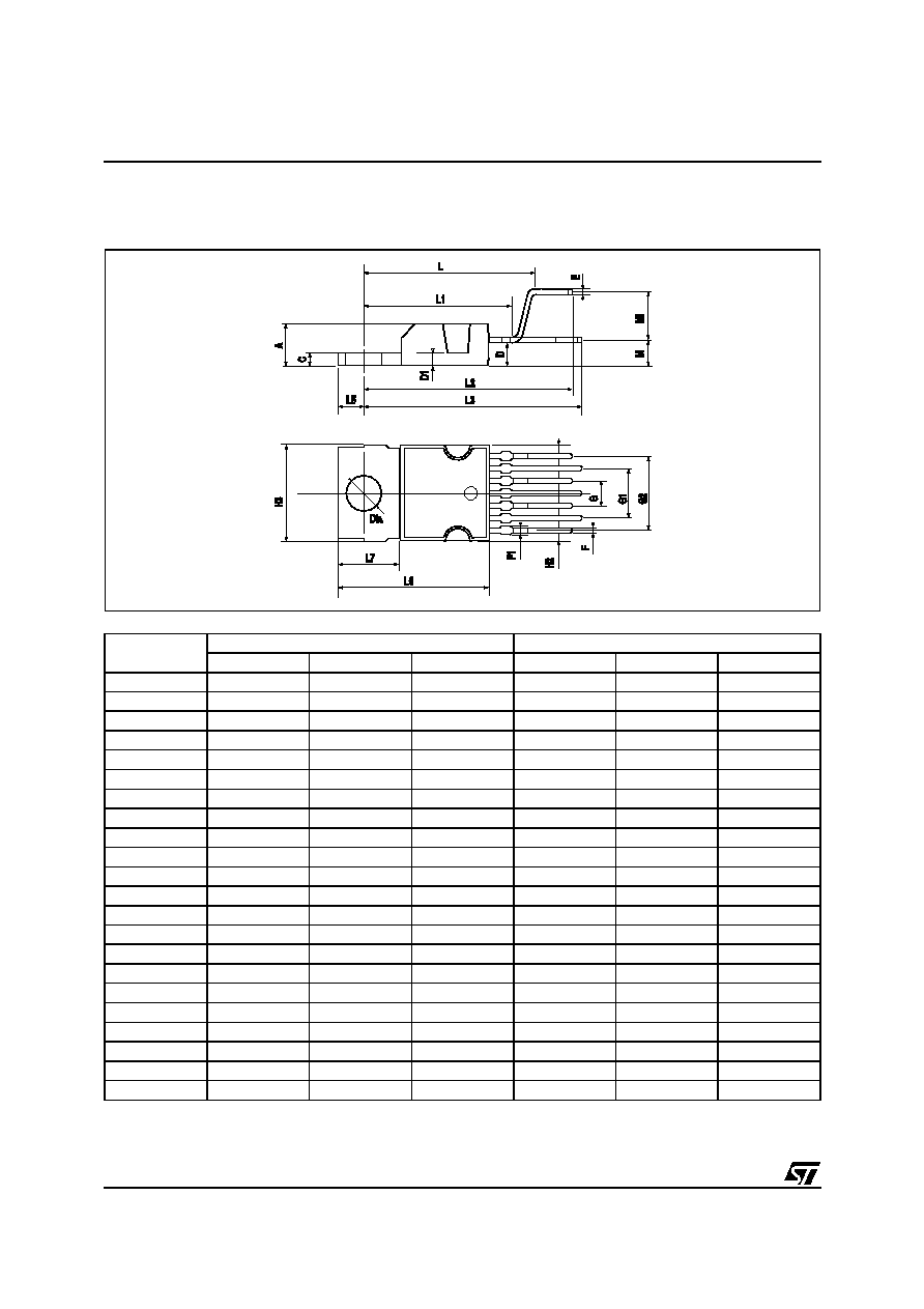
PACKAGE MECHANICAL DATA
9-PINS - PLASTIC HEPTAWATT
Figure 4. 9-Pin Package
Dimensions
Millimeters
Inches
Min.
Typ.
Max.
Min.
Typ.
Max.
A
4.8
0.189
C
1.37
0.054
D
2.4
2.8
0.094
0.110
D1
1.2
1.35
0.047
0.053
E
0.35
0.55
0.014
0.022
F
0.6
0.8
0.024
0.031
F1
0.9
0.035
G
2.41
2.54
2.67
0.095
0.100
0.105
G1
4.91
5.08
5.21
0.193
0.200
0.205
G2
7.49
7.62
7.80
0.295
0.300
0.307
H2
10.4
0.409
H3
10.05
10.40
0.396
0.409
L
16.97
0.668
L1
14.92
0.587
L2
21.54
0.848
L3
22.62
0.891
L5
2.6
3.0
0.102
0.118
L6
15.10
15.80
0.594
0.622
L7
6.0
6.6
0.236
0.260
M
2.8
0.110
M1
5.08
0.200
Dia.
3.65
3.85
0.144
0.152
1

STV8131
5/5
Information furnished is believed to be accurate and reliable. However, STMicroelectronics assumes no responsibility for the consequences
of use of such information nor for any infringement of patents or other rights of third parties which may result from its use. No license is granted
by implication or otherwise under any patent or patent rights of STMicroelectronics. Specifications mentioned in this publication are subject
to change without notice. This publication supersedes and replaces all information previously supplied. STMicroelectronics products are not
authorized for use as critical components in life support devices or systems without the express written approval of STMicroelectronics.
The ST logo is a registered trademark of STMicroelectronics
©
2003 STMicroelectronics - All Rights Reserved.
Purchase of I
2
C Components by STMicroelectronics conveys a license under the Philips I
2
C Patent. Rights to use these components in an
I
2
C system is granted provided that the system conforms to the I
2
C Standard Specification as defined by Philips.
STMicroelectronics Group of Companies
Australia - Brazil - China - Finland - France - Germany - Hong Kong - India - Italy - Japan - Malaysia - Malta - Morocco - Singapore - Spain
Sweden - Switzerland - United Kingdom - U.S.A.
http://www.st.com
1