 | –≠–ª–µ–∫—Ç—Ä–æ–Ω–Ω—ã–π –∫–æ–º–ø–æ–Ω–µ–Ω—Ç: STV8163 | –°–∫–∞—á–∞—Ç—å:  PDF PDF  ZIP ZIP |

STV8163
+3.3 V, +5 V and Adjustable Triple-Voltage Regulator
with Disable and Reset Functions
Æ
September 2003
1/11
FEATURES
s
Input Voltage range between 5V and 18V,
limited to V
OUT
+ 6.5V
s
Maximum Available Output Currents greater than
0.8 A
s
Fixed Precision Output 1 voltage of 3.3 V ± 2% (at
10 mA)
s
Fixed Precision Output 2 voltage of 5 V ± 2% (at
10 mA)
s
Programmable Output 3 voltage: 2.5 to 16 V ± 2%
s
Output 1 with Reset facility
s
Outputs 2 and 3 can be disabled by digital input
s
Short Circuit Protection on each output
s
Thermal Protection
s
Low Dropout Voltages
DESCRIPTION
The STV8163 is a monolithic triple positive voltage
regulator designed to provide fixed precision output
voltages of 3.3 V, 5 V and an adjustable voltage for
currents up to 0.6 A.
The adjustable value of the third output can be fixed
from 2.5 V to 16 V.
An internal reset circuit generates a reset pulse
when the voltage of Output 1 drops below the
regulated voltage value.
Outputs 2 and 3 can be disabled by a digital input.
Short-circuit and thermal protections are included in
all versions.
Clipwatt11
(Plastic Package)
Order Code: STV8163
PROGRAM
9
8
7
6
5
4
3
2
1
INPUT3
OUTPUT3
INPUT2
GROUND
OUTPUT2
INPUT1
OUTPUT1
DELAY CAPACITOR
RESET
11
DISABLE
10
STV8163
2/11
TABLE OF CONTENTS
Chapter 1
GENERAL INFORMATION . . . . . . . . . . . . . . . . . . . . . . . . . . . . . . . . . . . . . . . . . .3
Chapter 2
ELECTRICAL CHARACTERISTICS . . . . . . . . . . . . . . . . . . . . . . . . . . . . . . . . . . . .4
2.1
Absolute Maximum Ratings ................................................................................................ 4
2.2
Thermal Data ...................................................................................................................... 4
2.3
Electrical Characteristics ...................................................................................................... 4
Chapter 3
CIRCUIT DESCRIPTION . . . . . . . . . . . . . . . . . . . . . . . . . . . . . . . . . . . . . . . . . . . . .6
3.1
Currents versus Maximum Power Limitation ........................................................................ 6
Chapter 4
APPLICATION DIAGRAM . . . . . . . . . . . . . . . . . . . . . . . . . . . . . . . . . . . . . . . . . . .8
Chapter 5
PACKAGE MECHANICAL DATA . . . . . . . . . . . . . . . . . . . . . . . . . . . . . . . . . . . . .9
Chapter 6
REVISION HISTORY . . . . . . . . . . . . . . . . . . . . . . . . . . . . . . . . . . . . . . . . . . . . . . .10
3/11
STV8163
GENERAL INFORMATION
1
GENERAL INFORMATION
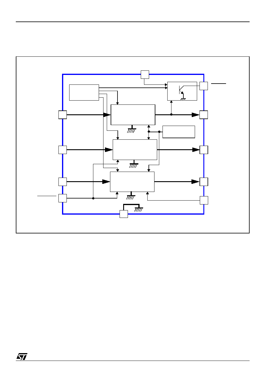
Figure 1: STV8163 Block Diagram
4
Regulator 1
1
3
Reference
INPUT1
OUTPUT1
RESET
DELAY CAPACITOR
2
Protections
7
Regulator 2
5
INPUT2
OUTPUT2
9
8
Regulator 3
11
10
INPUT3
DISABLE
OUTPUT3
PROGRAM
GROUND
6
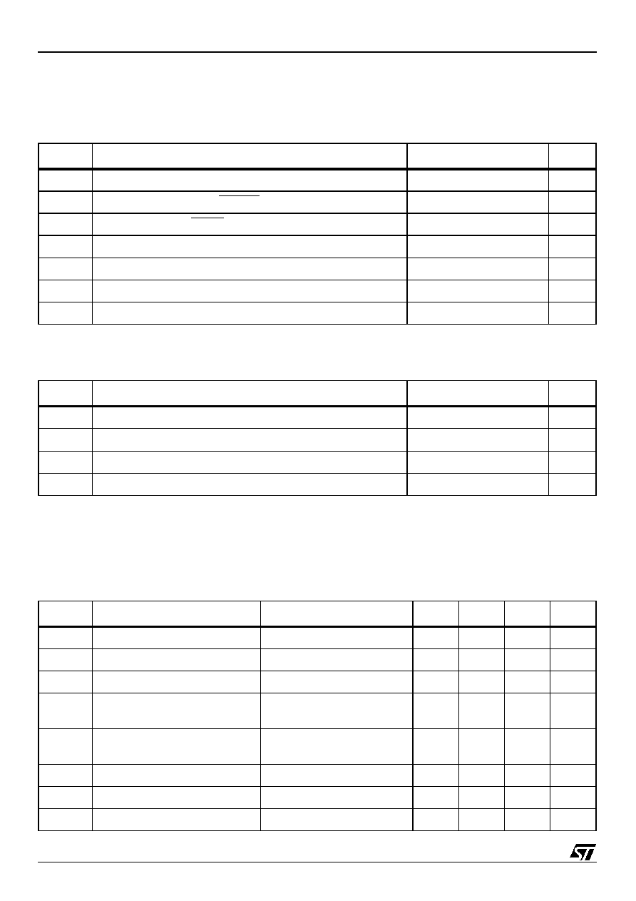
ELECTRICAL CHARACTERISTICS
STV8163
4/11
2
ELECTRICAL CHARACTERISTICS
2.1
Absolute Maximum Ratings
2.2
Thermal Data
2.3
Electrical Characteristics
T
AMB
= 25∞ C, V
IN1
= 5.3 V, V
IN2
= 7 V and V
IN3
= 10 V, unless otherwise specified.
Symbol
Parameter
Value
Unit
V
IN
DC Input Voltage at pins INPUT1, INPUT2 and INPUT3
20
V
V
DIS
Disable Input Voltage at pin DISABLE
20
V
V
RST
Output Voltage at pin RESET
20
V
I
OUTPUT
Output Currents
Internally Limited
P
t
Power Dissipation
Internally Limited
T
STG
Storage Temperature
-65 to +150
∞C
T
J
Junction Temperature
0 to +150
∞C
Symbol
Parameter
Value
Unit
R
thJC
Thermal Resistance (Junction-to-Case)
3
∞C/W
R
thJA
Thermal Resistance (Junction-to-Ambient)
10
1
1. Depending on heat sink conditions.
∞C/W
T
J
Maximum Recommended Junction Temperature
140
∞C
T
OPER
Operating Free Air Temperature Range
0 to +70
∞C
Symbol
Parameter
Test Conditions
Min.
Typ.
Max.
Unit
V
OUT1
Output Voltage
I
OUT1
= 10 mA
3.24
3.30
3.36
V
V
OUT2
Output Voltage
I
OUT2
= 10 mA
4.90
5.00
5.10
V
V
OUT3
Output Voltage
I
OUT3
= 10 mA
2.5
16
V
V
OUT1
Output Voltage
5.3 V < V
IN1
< 10 V
5 mA < I
OUT1
< 600 mA
3.18
3.42
V
V
OUT2
Output Voltage
7 V < V
IN2
< 12 V
5 mA < I
OUT2
< 600 mA
4.80
5.20
V
V
IO1
Dropout Voltage
I
OUT1
= 0.6 A
1
1.4
V
V
IO2
Dropout Voltage
I
OUT2
= 0.6 A
1
1.4
V
V
IO3
Dropout Voltage
I
OUT3
= 0.6 A
1
1.4
V
5/11
STV8163
ELECTRICAL CHARACTERISTICS
V
OUT1LI
Line Regulation
5.3 V < V
IN1
< 10 V,
I
OUT1
= 200 mA
30
mV
V
OUT2LI
Line Regulation
7 V < V
IN2
< 12 V,
I
OUT2
= 200 mA
50
mV
V
OUT3LI
Line Regulation
10 V < V
IN3
< 15 V,
I
OUT3
= 200 mA, V
OUT3
= 8 V
80
mV
V
OUT1LO
Load Regulation
5 mA < I
OUT1
< 600 mA
100
mV
V
OUT2LO
Load Regulation
5 mA < I
OUT2
< 600 mA
100
mV
V
OUT3LO
Load Regulation
5 mA < I
OUT3
< 600 mA,
V
OUT3
= 8 V
160
mV
I
Q
Quiescent Current
I
OUT1
= 10 mA
Outputs 2 and 3 disabled
2.2
3.0
mA
V
O1RST
Reset Threshold Voltage
1
K = V
OUT1,
I
OUT1
> 50 mA
K-0.4
K-0.25
K-0.10
V
V
RTH
Reset Threshold Hysteresis
See circuit description.
30
75
120
mV
t
RD
Reset Pulse Delay
C
E
= 100 nF
See circuit description.
25
ms
V
RL
Saturation Voltage in Reset
Condition
I
RESET
= 5 mA
0.4
V
I
RH
Leakage Current in Normal
Condition, at RESET pin
V
RESET
= 10 V
10
µ
A
K
OUT1
K
OUT2
K
OUT3
Output Voltage Thermal Drift
T
J
= 0 to 125∞C
100
ppm/∞C
I
OUT1SC
Short Circuit Output Current
V
IN1
= 5.3 V
0.8
1.3
1.8
A
I
OUT2SC
Short Circuit Output Current
V
IN2
= 7 V
0.8
1.3
1.8
A
I
OUT3SC
Short Circuit Output Current
V
IN3
= V
OUT3
+ 2V
0.8
1.3
1.8
A
V
PROG
Input Voltage at PROGRAM pin
2
V
I
PROG
Input Current at PROGRAM pin
5
µ
A
V
DISH
Voltage High Level at DISABLE pin (Outputs 2 and 3 active)
2
V
V
DISL
Voltage Low Level at DISABLE pin (Outputs 2 and 3 disabled)
0.8
V
I
DIS
Bias Current at DISABLE pin
0 V < V
DISABLE
< 5.3 V
-100
2
µ
A
T
JSD
Junction Temperature for Thermal Shutdown
150
∞C
T
SDH
Thermal Shutdown Temperature Hysteresis
15
∞C
1. This reset signal is activated by a decrease of V
OUT1
voltage which can be due to an overload of pin OUT1
or by a lack of Input Voltage (VIN1).
Symbol
Parameter
Test Conditions
Min.
Typ.
Max.
Unit
K
OUT
V
OUT
10
6
T V
OUT
--------------------------------
=