 | –≠–ª–µ–∫—Ç—Ä–æ–Ω–Ω—ã–π –∫–æ–º–ø–æ–Ω–µ–Ω—Ç: STV8226 | –°–∫–∞—á–∞—Ç—å:  PDF PDF  ZIP ZIP |
DATASHEET
Æ
STV82x6
Multistandard TV Audio Processor
and Digital Sound Demodulator
February 2005
1/97
Rev. 3
This device incorporates the
SRS (Sound Retrieval
System) under licence from
SRS Labs, Inc.
Key Features
NICAM, AM, FM Mono and FM 2 Carrier
Stereo Demodulators for all sound carriers
between 4.5 and 7 MHz
Mono input provided for optimum AM
Demodulation performances
Demodulation controlled by Automatic
Standard Recognition System
Sound IF AGC with wide range
Overmodulation and Carrier Offset recovery
Smart Volume Control
5-band Equalizer & Bass/Treble Control
Automatic Loudness Control
Loudspeaker and Headphone outputs with
Volume/Balance Controls and Beeper
Subwoofer output with Volume Control and
Programmable Bandwidth
Spatial Sound Effects
(ST WideSurround and
Pseudo-Stereo)
SRSÆ 3D Surround
3-to-2 Analog Stereo Audio I/Os (SCART
compatible) with Audio Matrix
Low-noise Audio Mutes and Switches
I≤S Output to interface with DolbyÆ Pro
Logic
Æ Decoder
I≤C Bus-controlled
Single and standard 27 MHz Crystal
Oscillator
Power supplies: 3.3 V Digital, 5 V or 8 V
Analog
Embedded 3.3 V Regulators
Packages: SDIP56 or TQFP80
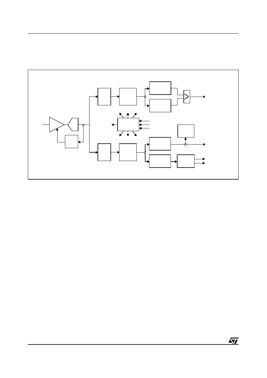
Audio
AGC
Audio
A/D
A/D
SDA
SCL
SIF
AI1L
AI1R
LSL
LSR
SW
Matrix
AI2L
AI2R
AI3L
AI3R
Input
Stereo
MONOIN
Multi-Standard
Demodulator
Digital
Audio
Matrix
Analog
Source Preprocessing
FM, AM, A2
and NICAM
Loudspeaker Audio Processing
Smart Volume Control, ST WideSurround,
5-band Equalizer and Loudness,
Headphone Audio Processing
Smart Volume Control,
Beeper and Subwoofer Output
Bass/Treble and Beeper
I≤S Interface
Audio
Stereo
D/A
Audio
Stereo
D/A
Audio
Stereo
D/A
Vol./
Low Noise
Audio Mute
1V
rms
HPL
HPR
Low Noise
Audio Mute
1V
rms
SCK
SDO
WS
I≤C Interface
Gain
Audio
Matrix
Output
Analog
Low Noise
Audio Mute
Low Noise
Audio Mute
2V
rms
2V
rms
AO1L
AO1R
AO2L
AO2R
IRQ
ST
BUS0
BUS1
HPD
0.5V
rms
2V
rms
2V
rms
2V
rms
Single Crystal
Clock Generation
Audio Matrixing
Audio Processing
Demodulation
XTI
XTO
Power Supply Management
DC Regulators, Standby mode
I≤C Bus Expander
Input SCARTs
Sound IF
Output Scarts
Headphone
Subwoofer
Loudspeaker
Headphone
Detection
Mono In
Stereo
Interrupt
STV82x6
Digital Stereo
Request
Flag
Stereo
Flag
Bal.
Vol./
Bal.

STV82x6
2/97
Table of Contents
Chapter 1
General Description . . . . . . . . . . . . . . . . . . . . . . . . . . . . . . . . . . . . . . . . . . . . . . . .5
1.1
Overview .............................................................................................................................. 5
1.2
Typical Applications ......................................................................................................... 6
1.3
I/O Pin Description ............................................................................................................. 10
Chapter 2
Demodulator Block . . . . . . . . . . . . . . . . . . . . . . . . . . . . . . . . . . . . . . . . . . . . . . .12
2.1
Digital Demodulator ............................................................................................................ 12
2.2
System Clock ..................................................................................................................... 16
Chapter 3
Audio Processor Block . . . . . . . . . . . . . . . . . . . . . . . . . . . . . . . . . . . . . . . . . . . .17
3.1
Main Features .................................................................................................................... 17
3.2
Smart Volume Control (SVC) ............................................................................................. 18
3.3
ST WideSurround ............................................................................................................... 19
3.4
5-Band Audio Equalizer ..................................................................................................... 19
3.5
Bass/Treble Control ........................................................................................................... 19
3.6
Volume/Balance Control .................................................................................................... 20
3.7
Automatic Loudness Control .............................................................................................. 22
3.8
Subwoofer Control ............................................................................................................. 22
3.9
Beeper ................................................................................................................................ 22
3.10
SRSTM 3D Surround (STV8226/36 only) ............................................................................ 23
Chapter 4
Audio Matrices . . . . . . . . . . . . . . . . . . . . . . . . . . . . . . . . . . . . . . . . . . . . . . . . . . .25
4.1
Input Audio Matrix .............................................................................................................. 26
4.2
Output Audio Matrix ........................................................................................................... 26
Chapter 5
Additional Controls and Flags . . . . . . . . . . . . . . . . . . . . . . . . . . . . . . . . . . . . . .27
5.1
Interrupt Request ............................................................................................................... 27
5.2
I≤C Bus Expander ............................................................................................................... 27
5.3
Stereo Flag ......................................................................................................................... 27
5.4
Headphone Detection ........................................................................................................ 27
Chapter 6
I≤S Interface . . . . . . . . . . . . . . . . . . . . . . . . . . . . . . . . . . . . . . . . . . . . . . . . . . . . . .28

3/97
STV82x6
Chapter 7
Power Supplies . . . . . . . . . . . . . . . . . . . . . . . . . . . . . . . . . . . . . . . . . . . . . . . . . . .29
7.1
Supply Voltages ................................................................................................................. 29
7.2
Standby Mode .................................................................................................................... 30
Chapter 8
I≤C Bus . . . . . . . . . . . . . . . . . . . . . . . . . . . . . . . . . . . . . . . . . . . . . . . . . . . . . . . . . .31
8.1
I≤C Address and Protocol ................................................................................................... 31
8.2
STV82x6 Reset .................................................................................................................. 31
Chapter 9
Register List . . . . . . . . . . . . . . . . . . . . . . . . . . . . . . . . . . . . . . . . . . . . . . . . . . . . .33
9.1
I≤C Register Map ................................................................................................................ 33
9.2
STV82x6 General Control Registers .................................................................................. 37
9.3
Analog Block ...................................................................................................................... 39
9.4
Clocking ............................................................................................................................. 41
9.5
Demodulator ....................................................................................................................... 43
9.6
Demodulator Channel 1 ..................................................................................................... 46
9.7
Demodulator Channel 2 ..................................................................................................... 49
9.8
NICAM Registers ............................................................................................................... 55
9.9
Zweiton ............................................................................................................................... 56
9.10
Sound Preprocessing and Selection Registers .................................................................. 57
9.11
Automatic Standard Recognition ........................................................................................ 64
9.12
Smart Volume Control ........................................................................................................ 68
9.13
Surround ............................................................................................................................ 70
9.14
5- Band Equalizer ............................................................................................................... 72
9.15
Loudness/Bass & Treble .................................................................................................... 74
9.16
Volume/Balance Control Registers .................................................................................... 76
9.17
Subwoofer .......................................................................................................................... 79
9.18
Beeper ................................................................................................................................ 80
Chapter 10
Input/Output Groups . . . . . . . . . . . . . . . . . . . . . . . . . . . . . . . . . . . . . . . . . . . . . .82
Chapter 11
Electrical Characteristics . . . . . . . . . . . . . . . . . . . . . . . . . . . . . . . . . . . . . . . . . .86
11.1
Absolute Maximum Ratings .............................................................................................. 86
11.2
Thermal Data .................................................................................................................... 86
11.3
Supply ................................................................................................................................ 86
11.4
Crystal Recommendations ................................................................................................ 87

STV82x6
4/97
11.5
Analog Sound IF Signal Recommendations ..................................................................... 87
11.6
SIF to LS/HP/SCART Path Characteristics ....................................................................... 88
11.7
SCART to SCART Analog Path Characteristics ............................................................... 88
11.8
SCART to I2S Output Path (via ADC) Characteristics ...................................................... 89
11.9
MONOIN to ADC and I2S Output Path Characteristics .................................................... 89
11.10
I2S to LS/HP/SW Path Characteristics ............................................................................. 89
11.11
I2S to SCART Path Characteristics .................................................................................. 90
11.12
Loudspeaker and Headphone Volume Control Characteristics ........................................ 90
11.13
MUTE Performance ........................................................................................................... 90
11.14
Digital I/Os ......................................................................................................................... 90
11.15
I≤C Bus Interface .............................................................................................................. 91
Chapter 12
Package Mechanical Data . . . . . . . . . . . . . . . . . . . . . . . . . . . . . . . . . . . . . . . . .93
Chapter 13
Revision History . . . . . . . . . . . . . . . . . . . . . . . . . . . . . . . . . . . . . . . . . . . . . . . . .95
5/97
STV82x6 General
Description
1
General Description
1.1
Overview
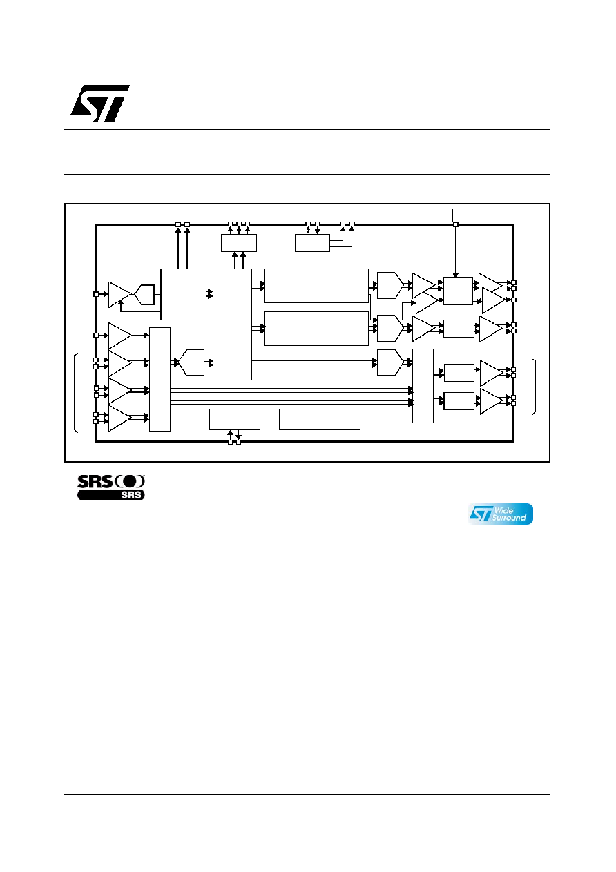
The STV82x6 is composed of three main parts:
1. TV Sound Demodulator: provides all the necessary circuitry for the demodulation of audio
transmissions of European and Asian terrestrial TV broadcasts. The various transmission
standards are automatically detected and demodulated without user intervention.
2. Audio Processor: based on DSP technology, independently controls loudspeaker, subwoofer
and headphone signals. It offers basic and advanced features, such as a ST WideSurround,
Equalizer, Automatic Loudness and Smart Volume Control for television viewer comfort. The
STV8226/36 versions can perform additionally the SRS
Æ 3D Surround for stereo and mono
signals.
3. Audio Matrix: 3 stereo and 1 mono external analog audio inputs to loudspeakers and
headphone, with 2 stereo external analog audio outputs (SCART compatible).
Table 1: STV82x6 Version List
Feature
STV8206
STV8216
STV8226
STV8236
AM-FM Mono
X
X
X
X
Zweiton
X
X
X
X
NICAM
X
X
ST WideSurround
X
X
X
X
SRS
Æ 3D Surround
X
X
Figure 1: Package Ordering Information
SDIP56 Package
Order Code: STV82x6D
TQFP80 Package
Order Code: STV82x6 (Tray)
STV82x6T (Tape & Reel)
General Description
STV82x6
6/97
1.2
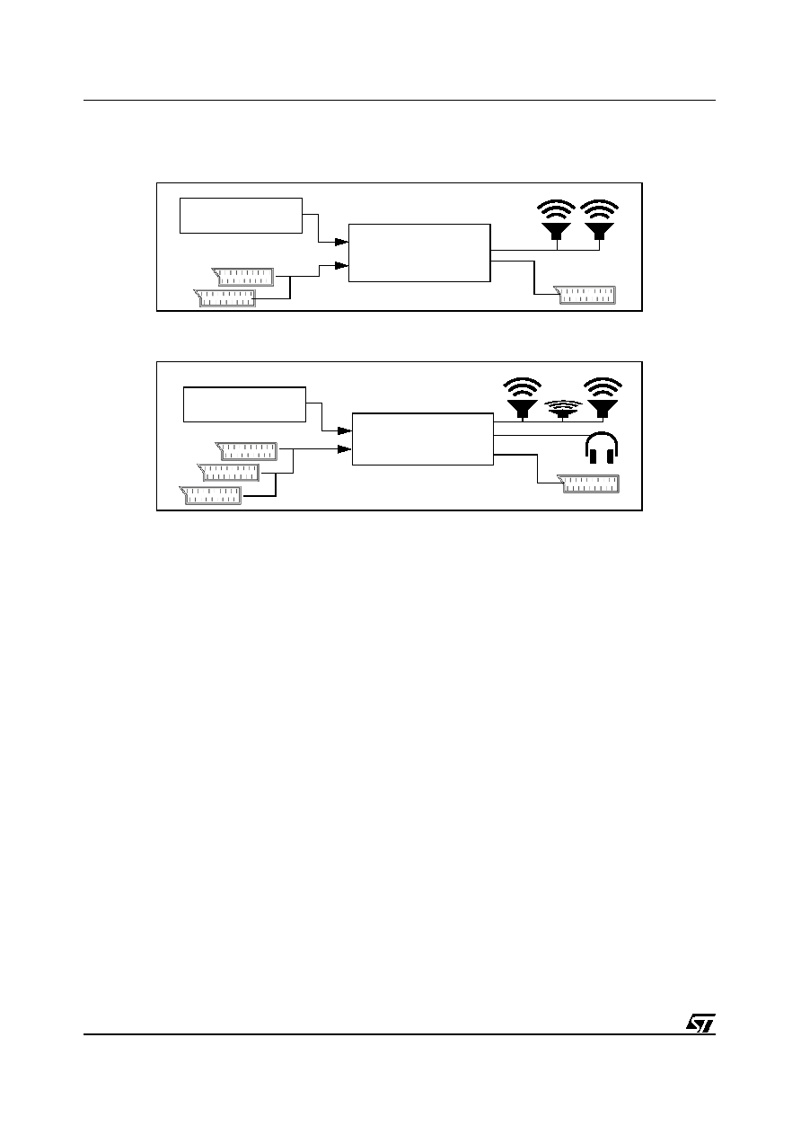
Typical Applications
Figure 2: Typical Application (Low-cost Stereo TV)
Figure 3: Typical Application with Subwoofer and Headphone
STV82x6
TV Sound Demodulation
and Audio Processing
Cable and Terrestrial
Analog TV Tuner
STV82x6
TV Sound Demodulation
and Audio Processing
Cable and Terrestrial
Analog TV Tuner
Woofer
7/97
STV82x6 General
Description
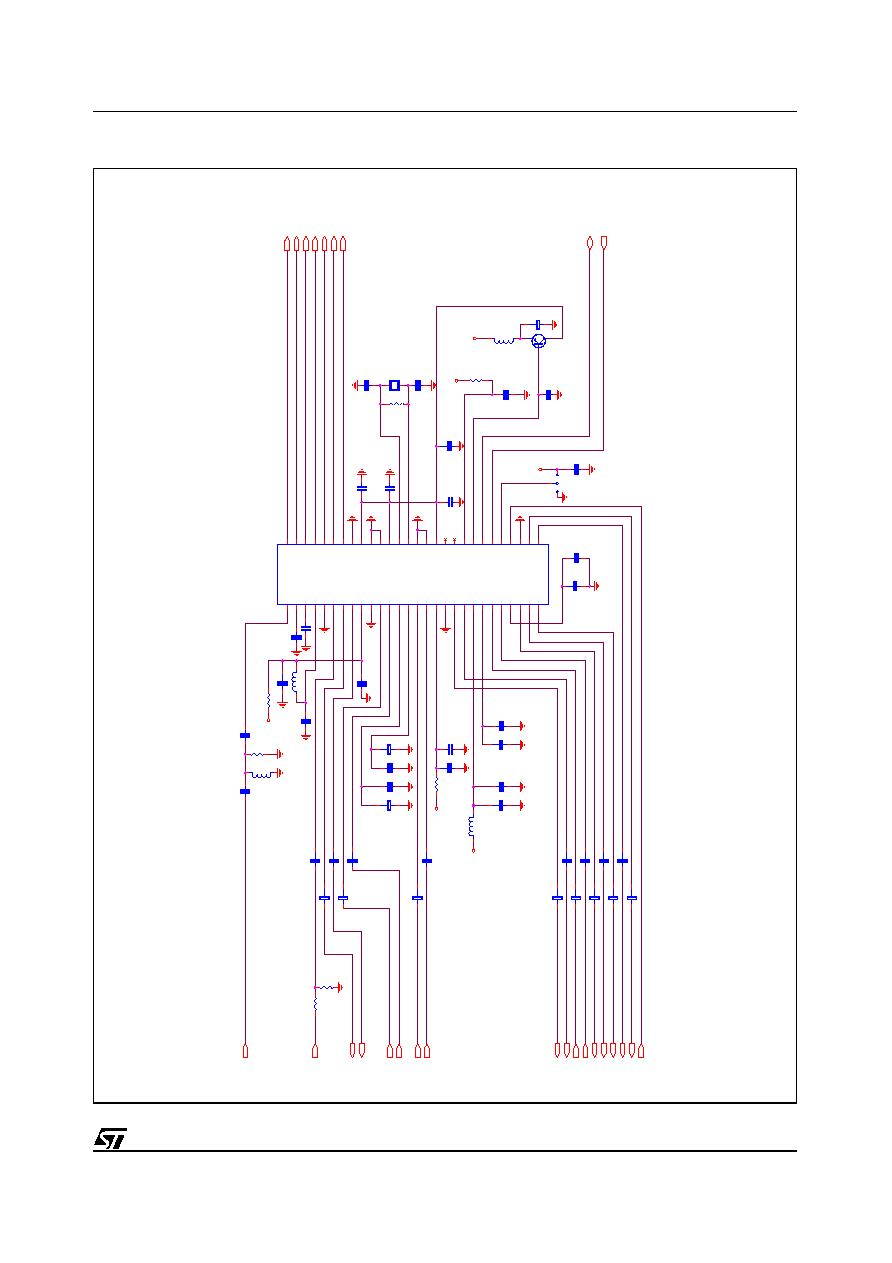
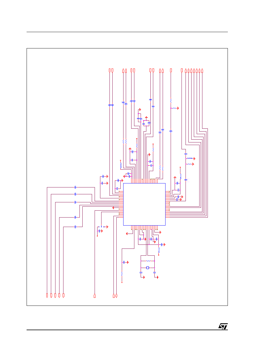
Figure 4: Typical Application Electrical Diagram for STV82x6 in SDIP56 package
MONO IN
SC1 OUT Left
SC1 OUT Right
SC1 IN Left
SC1 IN Right
SC2 OUT Left
SC2 OUT Right
LSL
SC2 IN Left
SC2 IN Right
SC3 IN Right
SC3 IN Left
LSR
Subwoofer
HPL
HPR
SIF
SCK
WS
STEREO ident
SDO
BUS1
IRQ
BUS0
HPD
SCL
SDA
+8V
+5V
+8V
+5V
+5V
+5V
RESET
SDIP56
Adress select
+
C31
10uF
+
C31
10uF
C32
100nF
C32
100nF
+
C11
1uF
+
C11
1uF
L2
10uH
L2
10uH
+
C41
1uF
+
C41
1uF
C12
22pF
C12
22pF
+
C10
1uF
+
C10
1uF
R10
22
R10
22
+
C38
1uF
+
C38
1uF
+
C3
10uF
+
C3
10uF
C4
220nF
C4
220nF
+
C17
47uF
+
C17
47uF
C20
100nF
C20
100nF
R13
330
R13
330
C14
100nF
C14
100nF
+
C7
1uF
+
C7
1uF
C22
100nF
C22
100nF
C21
100nF
C21
100nF
R9
560
R9
560
3
2
1
T1
BC327-40
T1
BC327-40
L3
10uH
L3
10uH
C39
220nF
C39
220nF
+
C19
10uF
+
C19
10uF
+
C26
10uF
+
C26
10uF
R12
10K
R12
10K
C5
100nF
C5
100nF
C2
10nF
C2
10nF
+
C30
10uF
+
C30
10uF
C1
100pF
C1
100pF
C40
100nF
C40
100nF
R14
100K
R14
100K
C46
100nF
C46
100nF
C6
100nF
C6
100nF
C29
470nF
C29
470nF
L1
10uH
L1
10uH
C13
100nF
C13
100nF
+
C37
10uF
+
C37
10uF
R11
10K
R11
10K
+
C36
10uF
+
C36
10uF
R15
270K
R15
270K
+
C44
1uF
+
C44
1uF
SIF
1
VTOP
2
VREFIF
3
VDDIF
4
GNDIF
5
MONOIN
6
AO1L
7
AO1R
8
VDCC
9
GNDC
10
AI1L
11
AI1R
12
VMC1
13
VMC2
14
AI2L
15
AI2R
16
VDDA
17
GNDAH
18
AO2L
19
AO2R
20
VDDH
21
VREFA
22
AI3L
23
AI3R
24
BGAP
25
LSL
26
LSR
27
SW
28
IRQ
56
BUS0
55
BUS1
54
SCK
53
WS
52
ST
51
SDO
50
CKTST
49
VDD2
48
GND2
47
GNDP
46
VDDP
45
XTO
44
XTI
43
GNDSP
42
GND1
41
VDD1
40
MCK
39
SYSCK
38
RESET
37
REG
36
SDA
35
SCL
34
ADR
33
HPD
32
GNDSA
31
HPR
30
HPL
29
IC1
STV82x6
IC1
STV82x6
C27
100nF
C27
100nF
C23
22pF
C23
22pF
+
C34
10µ
F
+
C34
10µ
F
+
C35
10uF
+
C35
10uF
+
C25
1uF
+
C25
1uF
1
2
XT1
27MHz
XT1
27MHz
+
C43
1uF
+
C43
1uF
+
C18
10uF
+
C18
10uF
+
C24
1uF
+
C24
1uF
+
C47
1uF
+
C47
1uF
+
C42
1uF
+
C42
1uF
C28
100nF
C28
100nF
1
2
3
ST1
ST1
+
C45
1uF
+
C45
1uF
+
C9
10uF
+
C9
10uF
L5
10uH
L5
10uH
+
C8
10uF
+
C8
10uF
C33
100nF
C33
100nF
General Description
STV82x6
8/97
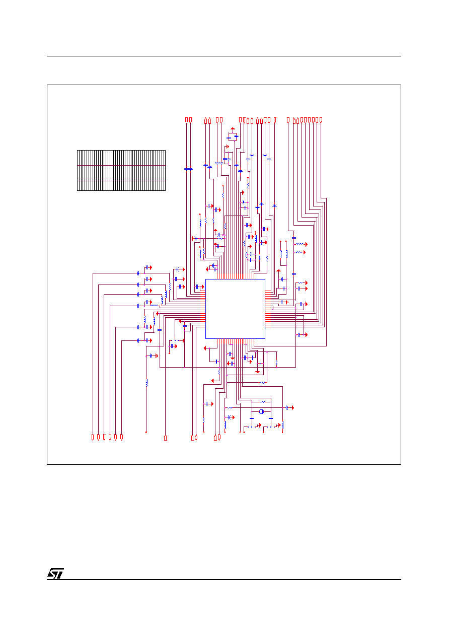
Figure 5: Typical Application Electrical Diagram for STV82x6 in TQFP80 package
SCL
Headphone detection
HP Left
Subwoofer
LS Right
LS Left
SIF
IRQ
BUS0
Mono IN
SC1 OUT Right
SC1 OUT Left
SC1 IN Right
SC1 IN Left
SC2 IN Right
SC2 IN Left
SC3 IN Left
SC3 IN Right
SC2 OUT Right
SC2 OUT Left
HP Right
SDA
BUS1
SCK
WS
STEREO ident
SDO
+3.3V
+3.3V
+8V
+8V
+8V
+3.3V
+3.3V
Address select
1
3
TQFP80
Reset
220
220
220
220
CRYSTAL
+
C4
1µ
F
+
C4
1µ
F
+
C56
10µ
F
+
C56
10µ
F
+
C5
1µ
F
+
C5
1µ
F
C25
100nF
C25
100nF
L11
10µH
L11
10µH
L4
10µ
H
L4
10µ
H
1
2
3
SL1
SL1
C31
100nF
C31
100nF
C50
100nF
C50
100nF
C12
100nF
C12
100nF
+
C76
10µ
F
+
C76
10µ
F
+
C6
1µ
F
+
C6
1µ
F
+
C17
47µ
F
+
C17
47µ
F
R5
R5
C57
100nF
C57
100nF
C58
100nF
C58
100nF
+
C77
10µ
F
+
C77
10µ
F
L7
10µ
H
L7
10µ
H
C26
100nF
C26
100nF
R12
75
R12
75
+
C53
1µ
F
+
C53
1µ
F
C35
100pF
C35
100pF
C32
220nF
C32
220nF
R8
R8
+
C54
1µ
F
+
C54
1µ
F
+
C49
10µ
F
+
C49
10µ
F
+
C79
10µ
F
+
C79
10µ
F
+
C7
1µ
F
+
C7
1µ
F
C33
100nF
C33
100nF
R3
560
R3
560
R4
R4
+
C40
10µ
F
+
C40
10µ
F
C52
100nF
C52
100nF
+
C45
1µ
F
+
C45
1µ
F
R1
100K
R1
100K
R10
330
R10
330
AO1L
1
AO1R
2
N/C
3
N/C
4
N/C
5
N/C
6
VDDC
7
GNDC
8
AI1L
9
AI1R
10
VMC1
11
N/C
12
VMC2
13
AI2L
14
AI2R
15
VDDA
16
GNDAH
17
AO2L
18
AO2R
19
VDDH
20
N/C
21
VREFA
22
AI3L
23
AI3R
24
N/C
25
BGAP
26
N/C
27
LSL
28
LSR
29
SW
30
HPL
31
HPR
32
GNDSA
33
N/C
34
HPD
35
ADR
36
N/C
37
N/C
38
SCL
39
SDA
40
N/C
41
REG
42
RESET
43
SYSCK
44
MCK
45
VDD1
46
GND1
47
N/C
48
GNDSP
49
N/C-
50
N/C
51
XTI
52
XTO
53
VDDP
54
GNDP
55
GND2
56
VDD2
57
CKTST
58
N/C
59
N/C
60
SDO
61
ST/SDI
62
WS
63
SCK
64
BUS1
65
N/C
66
N/C
67
BUS0
68
IRQ
69
N/C
70
N/C
71
N/C
72
SIF
73
VTOP
74
VREFIF
75
VDDIF
76
GNDIF
77
MONOIN
78
N/C
79
N/C
80
IC1
STV82x6
IC1
STV82x6
+
C55
10µ
F
+
C55
10µ
F
+
C8
1µ
F
+
C8
1µ
F
+
C61
1µ
F
+
C61
1µ
F
R6
10K
R6
10K
+
C51
10µ
F
+
C51
10µ
F
+
C36
1µ
F
+
C36
1µ
F
C22
22pF
C22
22pF
C19
100nF
C19
100nF
+
C39
10µ
F
+
C39
10µ
F
C63
100nF
C63
100nF
+
C41
10µ
F
+
C41
10µ
F
L2
10µ
H
L2
10µ
H
C21
22pF
C21
22pF
+
C60
1µ
F
+
C60
1µ
F
+
C59
10µ
F
+
C59
10µ
F
C14
100nF
C14
100nF
XT1
27MHz
XT1
27MHz
R7
10K
R7
10K
R9
R9
+
C78
10µ
F
+
C78
10µ
F
R2
270k
R2
270k
C44
100nF
C44
100nF
+
C46
1µ
F
+
C46
1µ
F
C34
10nF
C34
10nF
C16
470nF
C16
470nF
9/97
STV82x6 General
Description
Figure 6: Typical Compatible Application Electrical Diagram for STV82x6 and STV82x7 in TQFP80 package
47 µF
R2
220
C68,C69
100 nF
*
between 2-3
Not Connected
Not Connected
R17
L15,L16
Not Connected
3
C70,C71
10 µF
*
Not Connected
L13,L14
R18
Part
0 ohm
C78
330pF
C3
C63
Note : comp
onents with * are only mandatory in case of DOLBY certification
10µH
100 nF
C15,C18
R19
R14
10 µF
Not Connected
TQFP80
220
L2
100 nF
strap
100 nF
10µH
100 nF
0 ohm
Not Connected
Not Connected
Not Connected
between 1-2
Reset
10µH
220
33 nF
100 nF
C21,C22
R15
100µH *
1 µF
with STV82x7
SL2
330pF
330 pF
10µH
330pF
C64,C65
Not Connected
22 pF
Not Connected
Not Connected
Not Connected
L3
100µH *
between 2-3
STV82x6 / STV82x7
330 pF
R11
STV82x6 / STV82x7 compatible Application El
ectrical Diagram
330pF
220
C41
27 pF
C59
Not Connected
0 ohm
R10
Not Connected
Not Connected
Not Connected
Not Connected
CRYSTAL
Not Connected
10 µF
with STV82x6
C23
10µH
0 ohm
330
C72,C73
L17,L18
between 1-2
330pF
33 nF
Not Connected
Not Connected
C9
*
R16
Not Connected
L5,L6
SL3
C74,C75
330pF
10 µF
C66,C67
47 µF
Not Connected
strap
Not Connected
R12
Not Connected
Not Connected
220
Not Connected
*
47 µF
C42
C27,C29
10µH
L1
330 µF
0 ohm
330 pF
Address select
220
C79
33 nF
*
strap
C43
C30
Not Connected
C10,C13
0 ohm
C76,C77
82
L4
270K
Not Connected
Not Connected
Not Connected
Not Connected
Not Connected
Not Connected
10 µF
10 µF
L8
100µH *
1
33 nF
Not Connected
*
0 ohm
C31
100 nF
0 ohm
Not Connected
R13
Not Connected
+3
.
3
V
+1
.
8
V
1.
8V
+8
V
+3
.
3
V
+1
.
8
V
+1
.
8
V
+8
V
+3
.
3
V
+1
.
8
V
+1
.
8
V
+8
V
+8
V
+3
.
3
V
+3
.
3
V
L6
10µH
R1
5
0
+
C7
1µF
+
C7
6
10µF
+
C7
8
10µF
+
C6
1µF
+
C2
3
47µF
C7
5
L5
10µH
+
C3
7
1µF
R1
470K
+
C3
1µF
L7
10µH
SL
2
1
2
3
C7
3
C1
0
100nF
+
C4
7
10µF
C6
4
33nF
C1
9
100nF
R1
3
0
+
C4
1µF
XT
1
27M
H
z
C3
4
22nF
+
C7
9
47µF
C7
1
R4
R1
9
0
C7
0
L8
10µH
L4
10µH
R1
8
0
C3
5
100pF
R5
+
C5
5
10µF
+
C6
1
1µF
+
C3
9
10µF
+
C5
9
47µF
L16
100µH
R1
0
330
R9
C6
9
33nF
L2
10µH
R2
270k
+
C4
3
10µF
IC1
1
2
3
4
5
6
7
8
9
10
11
12
13
14
15
16
17
18
19
20
21
22
23
24
25
26
27
28
29
30
31
32
33
34
35
36
37
38
39
40
41
42
43
44
45
46
47
48
49
50
51
52
53
54
55
56
57
58
59
60
61
62
63
64
65
66
67
68
69
70
71
72
73
74
75
76
77
78
79
80
AO
1
L
AO
1
R
N/
C
N/
C
N/
C
N/
C
V
DDC
G
NDC
AI
1
L
AI
1
R
VM
C
1
N/
C
VM
C
2
AI
2
L
AI
2
R
V
DDA
G
NDA
H
AO
2
L
AO
2
R
V
DDH
N/C
VREF
A
AI3
L
AI3
R
N/C
BGAP
N/C
LSL
LSR
SW
HPL
HPR
GNDS
A
N/C
HPD
ADR
N/C
N/C
SCL
SDA
N/
C
RE
G
RE
S
E
T
SYSC
K
MC
K
VD
D
1
G
ND1
N/
C
G
NDS
P
N/
C
N/
C
XT
I
XT
O
VD
D
P
G
NDP
G
ND2
VD
D
2
CK
T
S
T
N/
C
N/
C
SDO
ST/S
DI
WS
SCK
BUS1
N/C
N/C
BUS0
IRQ
N/C
N/C
N/C
SIF
VTO
P
VREF
IF
VDDIF
GNDIF
MON
OIN
N/C
N/C
R6
C7
4
C5
8
100nF
+
C9
330µF
L17
100µH
C3
2
220nF
C6
3
+
C6
0
1µF
+
C4
1
10µF
+
C4
9
10µF
C1
4
100nF
L18
100µH
C3
3
100nF
C4
2
100nF
C2
7
100nF
L3
10µH
C6
2
33nF
+
C5
3
1µF
+
C1
7
10µF
R8
C1
3
100nF
C4
4
100nF
L13
100µH
C5
7
100nF
L15
100µH
+
C
3
6
1µF
C2
6
100nF
+
C4
5
1µF
L11
10µH
C2
2
+
C4
0
10µF
+
C5
1µF
SL
1
1
2
3
C1
2
100nF
C6
8
33nF
C1
6
470nF
C6
6
33nF
C5
0
100nF
R1
7
0
C2
9
100nF
+
C8
1µF
C2
5
100nF
R7
C1
5
100nF
+
C5
1
10µF
C7
2
C2
1
+
C3
8
1µF
R1
6
0
C1
8
100nF
+
C7
7
10µF
R1
2
82
C3
1
100nF
C3
0
100nF
L1
10µH
R3
560
C6
5
33nF
SL
3
1
2
3
+
C4
6
1µF
+
C4
8
10µF
R1
1
0
R1
4
0
L14
100µH
C6
7
33nF
C
5
2
100nF
+
C5
4
1µF
+
C5
6
10µF
S
C
2 I
N
Lef
t
I
2
S SC
L
K
/
SD
O
H
eadphone det
ec
t
i
on
S
C
3 OU
T
R
i
ght
I
2
S L
R
C
L
K /
SD
I
S
C
1 I
N
Lef
t
S
P
D
IF
IN
S
C
1 OU
T
Lef
t
LS
Lef
t
LS
R
i
ght
I2
S
DA
T
A
0
/
W
S
S
C
3 I
N
Lef
t
S
C
3 I
N
R
i
ght
SC
L
S
C
4 I
N
Lef
t
SI
F
S
C
2 OU
T
R
i
ght
S
C
2 I
N
R
i
ght
IRQ
I
2
S D
A
T
A
2
/
BU
S1
H
P
Lef
t
/
L
S
s
u
rround Lef
t
BU
S EX
PAN
D
E
R
/
BU
S0
S
C
4 I
N
R
i
ght
LS
C
ent
er
S
C
2 OU
T
Lef
t
M
ono I
N
H
P
R
i
ght
/
L
S
s
u
rround R
i
ght
I2
S
P
C
M
CL
K
S
C
1 OU
T
R
i
ght
SPD
I
F
O
U
T
S
ubw
oof
er
SD
A
I
2
S
D
A
T
A
1
/ S
C
K
S
C
1 I
N
R
i
ght
S
C
3 OU
T
Lef
t
General Description
STV82x6
10/97
1.3
I/O Pin Description
Legend / Abbreviations for
Table 2
:
Type:
AP = Analog Power Supply
DP = Digital Power Supply
I =
Input
O
= Output
OD = Open Drain
B =
Bidirectional
A =
Analog
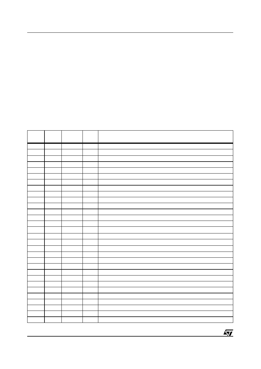
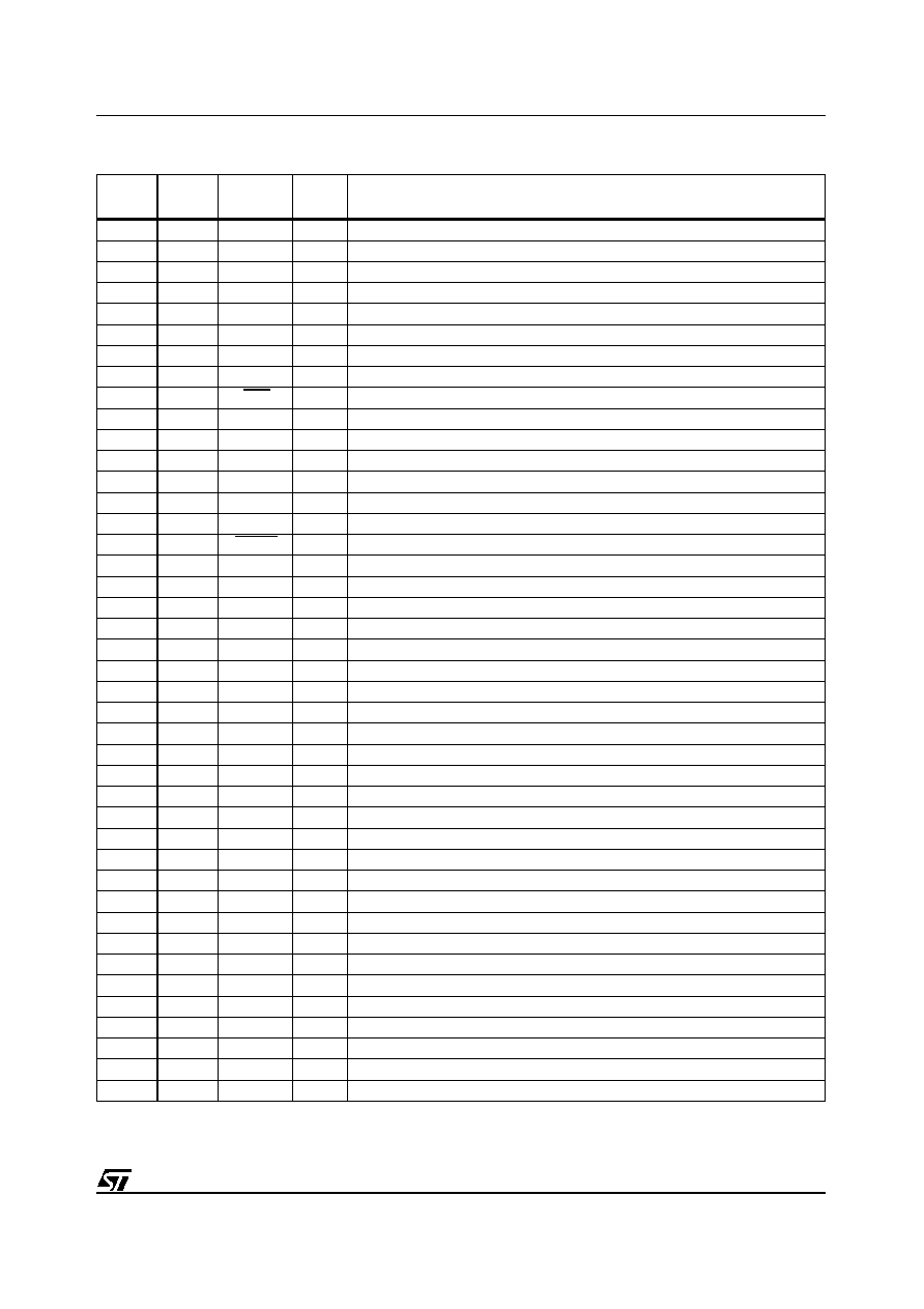
Table 2: Pin Description
SDIP
56
TQFP
80
Name
Type
Function
1
73
SIF
A
Sound IF Input
2
74
VTOP
A
ADC V
TOP
Decoupling Pin
3
75
VREFIF
A
AGC Voltage Reference Decoupling Pin
4
76
VDDIF
AP
3.3 V Power Supply for IF AGC & ADC
5
77
GNDIF
AP
0 V Power Supply for IF AGC & ADC
6
78
MONOIN
A
Mono Input
79/80
N/C
Not Used
7
1
AO1L
A
Left SCART1 Audio Output
8
2
AO1R
A
Right SCART1 Audio Output
-
3/4/5/6
N/C
Not used
9
7
VDDC
AP
3.3 V Power Supply for Audio DAC/ADC
10
8
GNDC
AP
0 V Power Supply for DAC/ADC
11
9
AI1L
A
Left SCART1 Audio Input
12
10
AI1R
A
Right SCART1 Audio Input
13
11
VMC1
A
Switched V
REF
Decoupling Pin for Audio Converters (VMCP)
-
12
N/C
Not used
14
13
VMC2
A
V
REF
Decoupling Pin for Audio Converters (VMC)
15
14
AI2L
A
Left SCART2 Audio Input
16
15
AI2R
A
Right SCART2 Audio Input
17
16
VDDA
AP
3.3 V Power Supply for Audio Buffers, Matrix & Bias
18
17
GNDAH
AP
0 V Power Supply for Audio Buffers & SCART
19
18
AO2L
A
Left SCART2 Audio Output
20
19
AO2R
A
Right SCART2 Audio Output
21
20
VDDH
AP
8 V / 5 V Power Supply for SCART & Audio Buffers
-
21
N/C
Not Used
22
22
VREFA
A
Voltage Reference for Audio Buffers
23
23
AI3L
A
Left SCART3 Audio Input
24
24
AI3R
A
Right SCART3 Audio Input
-
25
N/C
Not Used
25
26
BGAP
A
Bandgap Voltage Source Decoupling
11/97
STV82x6 General
Description
-
27
N/C
Not Used
26
28
LSL
A
Left Loudspeaker Output
27
29
LSR
A
Right Loudspeaker Output
28
30
SW
A
Subwoofer Output
29
31
HPL
A
Left Headphone Output
30
32
HPR
A
Right Headphone Output
31
33
GNDSA
AP
Substrate Analog/Digital Shield
-
34
N/C
Not Used
32
35
HPD
B
Headphone Detection Input (Active Low)
33
36
ADR
I
Hardware I≤C Chip Address Control
-
37/38
N/C
Not Used
34
39
SCL
OD
I≤C Serial Clock
35
40
SDA
OD
I≤C Serial Data
-
41
N/C
Not Used
36
42
REG
A
5 V Power Regulator Control
37
43
RESET
I
Hardware Reset (Active Low)
38
44
SYSCK
B
System Clock Output
39
45
MCK
B
I≤S Master Clock Output
40
46
VDD1
DP
3.3V Power Supply for Digital Core & IO Cells
41
47
GND1
DP
0V Power Supply for Digital Core & IO Cells
-
48
N/C
Not Used
42
49
GNDSP
AP
Substrate Analog/Digital Shield for Clock-PLL
50/51
N/C
Not Used
43
52
XTI
I
Crystal Oscillator Input
44
53
XTO
O
Crystal Oscillator Output
45
54
VDDP
AP
3.3 V Power Supply for Analog PLL Clock
46
55
GNDP
AP
0 V Power Supply for Analog PLL Clock
47
56
GND2
DP
0 V Power Supply for Digital Core, DSPs & IO Cells
48
57
VDD2
DP
3.3 V Power Supply for Digital Core, DSPs & IO Cells
49
58
CKTST
I
Must be Connected to 0 V
-
59/60
N/C
Not Used
50
61
SDO
B
I≤S Bus Data Output
51
62
ST/SDI
B
Stereo Detection Output / I≤S Bus Data Input
52
63
WS
B
I≤S Bus Word Select Output
53
64
SCK
B
I≤S Bus Clock Output
54
65
BUS1
B
I≤C Bus Expander Output 1
-
66/67
N/C
Not Used
55
68
BUS0
B
I≤C Bus Expander Output 2
56
69
IRQ
B
I≤C Status Read Request
-
70
N/C
Not Used
-
71
N/C
Not Used
-
72
N/C
Not Used
Table 2: Pin Description (Continued)
SDIP
56
TQFP
80
Name
Type
Function
Demodulator Block
STV82x6
12/97
2
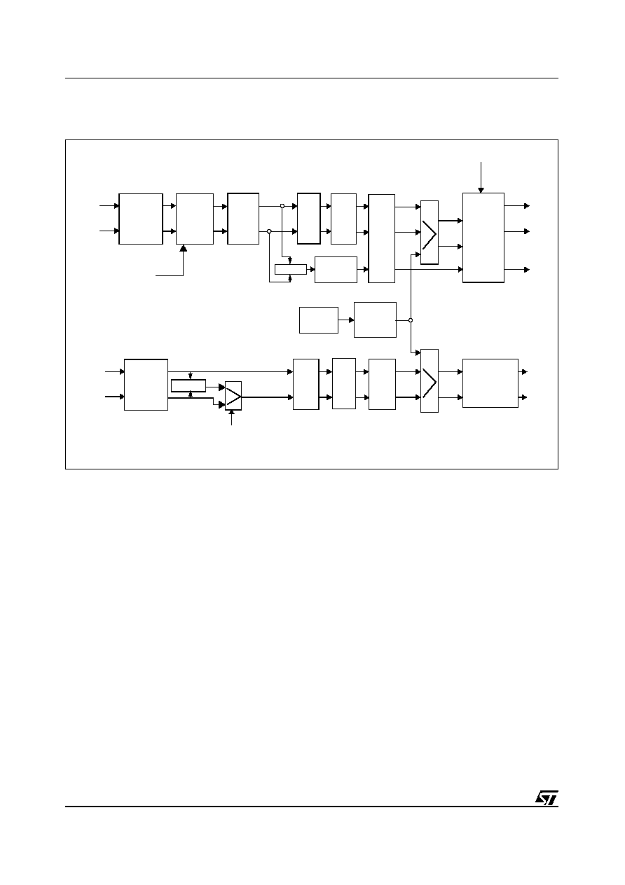
Demodulator Block
Note:
Zweiton is the Dual (Two Tone) FM stereo or A2 system.
2.1
Digital Demodulator
2.1.1
Sound IF Signal
The Analog Sound Carrier IF is connected to STV82x6 via the SIF pin. Before Analog-to-Digital
Conversion (ADC), an Automatic Gain Control (AGC) is performed to adjust the incoming IF signal
to the full scale of the ADC. A preliminary video rejection is recommended to optimize conversion
and demodulation performances. The AGC system provides a wide range of SIF input levels and is
activated for all standards, except L/L'. In this particular case, the sound carrier is AM-modulated
and an automatic level adjustment would only damage transmitted audio signal. A preset I≤C
parameter is required to define the gain of the AGC used in Manual mode (Registers
AGCC
and
AGCS
).
2.1.2
Demodulation
The demodulation system operates by default in Automatic mode. In this mode, the STV82x6 is able
to identify and demodulate any TV sound standard including NICAM and A2 systems (see
Table 2
) without any external control via the I≤C interface. It consists of the two demodulation
channels (Channel 1 = Mono Left and Channel 2 = Mono Right/Stereo) to simultaneously process
two sound carriers in order to handle all transmission modes (stereo and up to three mono
languages). The built-in Automatic Standard Recognition System (AUTOSTD) automatically
programs the appropriate bits in the I≤C registers which are forced to Read-only mode for users (see
Section 9.1
). The programming is optimized for each standard to be identified and demodulated.
Figure 7: Demodulator Block Diagram
Mixer
Mixer
DCO2 +
Channel
Filter
FIR1
Channel
Filter
FIR2
AM
Demodulator
FM
Demodulator
FM
Demodulator
DQPSK
Demodulator
AUTOSTD
AGC
Control
SIF
NICAM
Decoder
DCO1+
Zweiton
A/D
NICAML
NICAMR
AM/FM Mono
AM
FML
FM Stereo
AUTO_CTRL(50h)
AUTO_SCKM(51h)
AUTO_SCKST(52h)
AUTO_STAT(54h)
DEMOD_STAT(0Dh)
ZWT_STAT(41h)
NICAM_STAT(3Fh)
CAROFFSET1(22h)
CAROFFSET2(3Ah)
Channel 1 = Mono Left
Channel 2 = Stereo/Mono Right
AGCC(0Eh)
AGCS(0Fh)
(To Sound Preprocessing)
(To Sound Preprocessing)
(To Sound Preprocessing)
Decoder
AGC
Amp
13/97
STV82x6 Demodulator
Block
Each mono and stereo standard can be removed (or added) from the List of Standards to be
recognized by programming registers
AUTO_SCKM
and
AUTO_SCKST
, respectively. The identified
standard is displayed in register
AUTO_STAT
and any change to standard is flagged to the host
system via pin IRQ. This flag must be reset by re-programming the MSBs of register
AUTO_CTRL
while checking the detected standard status by reading registers
AUTO_STAT
,
NICAM_STAT
and
ZWT_STAT
. Moreover, the detection of Stereo mode during demodulation is also flagged in register
AUTO_STAT
and on output pin ST.
Important: L/L' and D/K standards cannot be automatically processed because the same frequency
is used for the MONO carrier. An exclusive L/DK selection must programmed in register
AUTO_CTRL
. This may be externally controlled by detecting the RF modulation sign, which is
negative for all TV standards except L/L'.
To recover out-of standard FM deviations or the Sound Carrier Frequency Offset, additional I≤C
controls are provided without interfering with the Automatic Standard Recognition System
(AUTOSTD).
DK-NICAM Overmodulation Recovery: Four different FM deviation ranges can be selected (via
register
AUTO_CTRL
) for the DK standard while the AUTOSTD system remains active. The
maximum FM deviation is 500 kHz in DK Mono mode and 350 kHz in DK NICAM mode (limited by
overlapping FM and NICAM spectrum values). The demodulated signal peak level (proportional to
the FM deviation) is detected by the Peak Detector and written to registers
PEAK_DET_STATL
and
PEAK_DET_STATR
. This value is used to implement Automatic Overmodulation Detection via an
external I≤C control.
Important: Only the selection of the 50 kHz FM deviation standard is compatible with the other DK-
A2* standards (DK1, DK2 or DK3). These standards must be removed from the list of standards
(registers
AUTO_SCKM
and
AUTO_SCKST
) when programming larger FM deviations reserved
only for DK-NICAM standards.
Table 3: Standards covered by the Automatic Standard Recognition System (AUTOSTD)
System
Sound Type
Type
Name
Carrier 1
(MHz)
Carrier 2
(MHz)
FM/AM Deviation
De-emphasis
Roll-
off
(%)
Pilot
Frequency
(kHz)
Min.
Typ.
Max.
M/N
FM Mono
4.5
15
27
50
75 µs
FM 2 Carriers
A2+
4.724
55.069
B/G
FM Mono
5.5
27
50
80
50 µs
FM/NICAM
5.850
J17
40
FM 2 Carriers
A2
5.742
50 µs
54.6875
I
FM Mono
6.0
27
50
80
50 µs
100
FM/NICAM
6.552
J17
100
L
AM Mono
6.5
0.5
1.0
AM/NICAM
5.850
J17
40
D/K
FM Mono
27
50
80
50 µs
FM/NICAM
5.850
J17
40
D/K1
FM 2 Carriers
A2*
6.258
50 µs
54.6875
D/K2
FM 2 Carriers
6.742
D/K3
FM 2 Carriers
5.742
Demodulator Block
STV82x6
14/97
Sound Carrier Frequency Offset Recovery: Both Mono and Stereo IF Carrier frequencies can be
adjusted independently (registers
CAROFFSET1
and
CAROFFSET2
) within a large range (up to
120 kHz for standard mono FM deviations) while the AUTOSTD system remains active. The
frequency offset estimation is written in registers
FM_DCL
and
FM_DCR
(Mono Left / Channel 1
And Mono Right / Channel 2, respectively) and can be used to implement the Automatic Frequency
Control (AFC) via an external I≤C control.
If required, the AUTOSTD system can be disabled (Manual mode) and the user can control all
registers including those only controlled by the AUTOSTD function when active. Manual mode is
selected in registers
RESET
or
AUTO_SCKM
.
2.1.3
Sound Preprocessing and Selection
The demodulated sound signal can be redirected to 4 different output audio channels:
1. Loudspeaker & Subwoofer,
2. Headphone,
3. SCART,
4. I≤S Interface.
Each output channel can independently select the demodulator source, analog SCART or I≤S inputs
using register
CH_SEL
.
Figure 8: Sound Preprocessing and Selection Block Diagram
DC
Prescaler
Dematrix
FM
FM
NICAM
I≤S OUT
Peak
Detector
FM/AM
AUDIO IN
(From Input Analog Audio Matrix)
(From Demodulator)
Cha
nne
l & La
ngu
age
S
e
lec
t
ion
LS IN
(To Loudspeaker Processing)
HP IN
(To Headphone Processing)
AUDIO OUT
(To Output Analog Audio Matrix)
(To I≤S Interface)
(From Demodulator)
PRE_FM(44h)
PRE_NICAM(45h)
PRE_AUX(46h)
PEAK_DET_CTRL(4Bh)
PEAK_DET_STATL(4Ch)
CH_MX(48h)
CH_SEL(49h)
CH_LANG(4Ah)
FM_DCL(42h)
FM_DCR(43h)
D
e
mod
u
la
tion
Mat
r
i
x
SC
A
R
T
Matrix
Removal
Prescaler
Dematrix
NICAM
NICAM
Prescaler
SCART
Di
gital
A
udi
o
Matri
x
De-emphasis
NICAM
De-emphasis
FM
I≤S IN
PRE_AUX(46h)
CH_MX(48h)
I≤S
Ma
trix
Prescaler
I≤S
PEAK_DET_STATR(4Dh)
15/97
STV82x6 Demodulator
Block
The level of the demodulated sound may require adjusting in order to compensate for the difference
in levels between the multiple source (NICAM, FM or AM) and standard source (FM deviation wide
range from 15 to 500 kHz) signals. The correct range for all level variations (+24 to -6 dB) is
selected in registers
PRE_FM
and
PRE_NICAM
. The internal sound level of the various sources
(FM/AM, NICAM and SCART) is read in registers
PEAK_DET_CTRL
,
PEAK_DET_STATL
and
PEAK_DET_STATR
before audio processing and can be used to implement Automatic Pre-scaling
via an external I≤C interface.
In Automatic mode, the STV82x6 selects and performs all appropriate de-emphasis, dematrixing,
sound selection and mute functions according to the standard and transmission mode detected.
Mono system: Mono audio signals received by an FM or AM carrier are demodulated. Left and
right audio outputs are identical. Automatic mute is applied when the mono standard cannot be
identified.
A2 systems (or Zweiton): Transmission of mono, stereo or bilingual audio signals using 2 separate
FM carriers + identification pilot. The pilot, transmitted by the second carrier, can be modulated by
two different tones in order to define Stereo or Dual-Mono mode. If not modulated, only the mono
signal is broadcast on the first carrier. Zweiton mode is read in register
ZWT_STAT
and described in
Table 4
. In the event of poor signal detection, the audio output is switched back to FM Mono mode
(backup). In Dual Mono mode, the language (A on Channel 1, B on Channel 2) can be selected
separately for each audio output channel (Loudspeaker, Headphone, SCART or I≤S) in register
CH_LANG
.
Note:
A2 and A2* standards are German Zweiton, while A2+ is Korean Zweiton.
NICAM systems: Transmission of mono, stereo, bilingual or trilingual audio signals using a
modulated-QPSK carrier and an FM/AM sound carrier backup. The digital QPSK modulation
broadcasts either channel stereo, dual mono, mono + data or data only. The selected NICAM mode
is read in register
NICAM_STAT
and described in
Table 5
. In the event of high bit-error rates, the
audio output is automatically switched back to the reserve sound transmission (FM/AM Mono) or
muted if there is no backup. In Dual Mono or Stereo mode with no backup, the language can be
selected separately for each audio output channel (Loudspeaker, Headphone, SCART or I≤S) in
register
CH_LANG
.
Table 4: A2 System Transmission Modes
System Mode
ZWT-STAT
[2:0]
FM Dematrix
FM
De-emphasis
CH_LANG
[1:0]
Sound
Selection
Sound
Backup
German Zweiton Mono
100
L,R
50 µs
XX
FM Mono
X
German Zweiton Stereo
110
(L+R)/2,R
50 µs
XX
FM Stereo
FM Mono
German Zweiton Dual
Mono (CH1=A, CH2=B)
101
L,R
50 µs
01
FM Mono A
X
10
FM Mono B
Mute
Korean Zweiton Mono
100
L,R
75 µs
XX
FM Mono
X
Korean Zweiton Stereo
110
(L+R)/2,(L-R)/2
75 µs
XX
FM Stereo
FM Mono
Korean Zweiton Dual Mono
(CH1 = A, CH2 = B)
101
L,R
75 µs
01
FM Mono A
X
10
FM Mono B
Mute
Zweiton undefined
0XX or 111
L,R
50 µs
XX
FM Mono
X
Demodulator Block
STV82x6
16/97
Note:
D1 and D2 define the two channels encoded in the NICAM packet.
2.2
System Clock
The System Clock integrates a low-jitter PLL clock and can be fully reprogrammed via registers
PLL_DIV
,
PLL_MD
,
PLL_PEH
and
PLL_PEL
. The default values are designed for a standard
27-MHz quartz crystal frequency, which is the recommended frequency for minimizing potential
RF interference in the application. This sinusoidal clock frequency, and any harmonic products,
remains outside the TV picture and sound IF (PIF/SIF) and Band-I RF passbands and has been
selected in order to reduce the risk of potential interference to the TV IF and RF system.
However, if required, the PLL clock can be re-programmed for an other quartz crystal frequency
within a range between 23 and 30 MHz.
Note:
A change in the crystal frequency is compatible with other default I≤C programming values,
including those of the built-in Automatic Standard Recognition System.
Table 5: NICAM System Transmission Modes
System Mode
NICAM_STAT[
4:1]
NICAM
De-emphasis
CH_LANG[1:0]
Sound
Selection
Sound
Backup
NICAM Stereo
1000
J17
XX
NICAM Stereo
FM/AM Mono
NICAM Dual Mono
(CH1 = A, CH2 = B)
1010
J17
01
NICAM Mono A
FM/AM Mono
10
NICAM Mono B
Mute
NICAM Mono+Data
(D1 = A, D2 = Data)
1001
J17
XX
NICAM Mono A
FM/AM Mono
NICAM Data
1011
J17
XX
FM/AM Mono
X
NICAM Stereo (no backup)
0000
J17
01
FM/AM Mono A
X
00
NICAM Stereo
Mute
NICAM Dual Mono (no backup) (D1
= B, D2 = C)
0010
J17
01
FM/AM Mono A
X
10
NICAM Mono B
Mute
11
NICAM Mono C
NICAM Mono+Data (no backup)
(D1 = B, D2 = Data)
0001
J17
01
FM/AM Mono A
X
10
NICAM Mono B
Mute
NICAM undefined (no backup)
X1XX
J17
XX
FM/AM Mono
X

17/97
STV82x6
Audio Processor Block
3
Audio Processor Block
3.1
Main Features
The STV82x6 Audio Processor is based on a dedicated audio Digital Signal Processor (DSP) that
performs basic and advanced audio post-processing for 4 different output audio channels.
3.1.1
Loudspeaker and Subwoofer Features
Smart Volume Control (See
Note 1
)
Spatial effects:
-- Pseudo Stereo (for Mono source)
-- ST WideSurround ("Movie" and "Music" modes for Stereo source)
5-band Equalizer
Volume and Balance controls (See
Note 4
)
Automatic Loudness control
Subwoofer (See
Note 4
)
Beeper (See
Note 3
)
Additionally on STV8226/36 only:
SRS
TM 3D Mono signal processing
SRS
TM 3D Stereo signal processing
3.1.2
Headphone
(See
Note 2
)
Smart Volume Control (See
Note 1
)
Bass and Treble controls
Volume and Balance controls
Beeper (See
Note 3
)
Note: 1 The Smart Volume Control can be used in either the loudspeaker or headphone path, but not both
at the same time.
2 The headphone is forced into Mono mode when the subwoofer is active.
3 The beeper is common for both the loudspeaker and the headphone.
4 The Auto-mute function is activated when a headphone plug is detected.
5 All audio postprocessing can be disabled.
3.1.3
SCART 1 and 2 Outputs
No audio post-processing
3.1.4
I≤S Output
No audio post-processing
Audio Processor Block
STV82x6
18/97
Note:
The audio signals available on the I≤S and SCART outputs are not affected by any digital or analog
matrix processing.
3.2
Smart Volume Control (SVC)
The Smart Volume Control (SVC) feature is designed to process sound level variations caused by
changes in signal sources (e.g. when switching channels) or in volume (e.g. when advertisements
are broadcast). The SVC is controlled by the SVC_ON bit in the
SVC_CTRL
register.
When the SVC_ON bit is set, the Smart Volume Control prevents annoying volume changes by
automatically adjusting the selected sound source (demodulator or SCART) to a programmable
reference level before audio processing. The regulation ranges from +6 dB to -30 dB with a fast
attenuation and a programmable slow amplification. The fast attenuation reduces audio peak (and
potential clipping) and slow amplification is a compromise between regulation recovery and limited
audio amplification during audio silence. The programmable output reference level must be defined
to prevent internal clipping depending on the selected audio processing boosting functions such as
Surround (up to +9 dB), Equalizer or Bass/Treble (up to +12 dB) and Loudness (up to +6 dB). When
the SVC is enabled, recommended reference values are -18 dB for the Loudspeaker path and -9 dB
for the Headphone path.
When the SVC is disabled, it acts as a wide-range prescaler (between -30 dB and +15.5 dB) before
audio-processing to prevent internal clipping depending on the selected functions (see above). If
Figure 9: Audio Processor Block Diagram
Equalizer
L
oudness
Spatial
Effects
Balance
Vo
lume
LS
IN
Volume
Lowpass
Beeper
Bass/
Woofer
Balance
Volume
SRS
1
0
(L+R)/2
(L+R)/2
Treble
5-band
(From
Di
gital
Au
dio
Ma
tri
x
)
Loudspeaker Processing
LS
OU
T
SW_ON
SW OUT
HP OU
T
Headphone Processing
Gain
HP IN
(
F
ro
m
D
i
gi
ta
l Audi
o Mat
r
ix)
Low
Audio
Audio Mute
Smart
Volume
Control
BEEPER_CTRL (79h)
BEEPER_TONE (7Ah)
SVC_SEL (59h)
SVC_CTRL (5Ah)
LS_EQ_CTRL (60h)
LS_EQ_BAND1 (61h)
LS_EQ_BAND2 (62h)
LS_EQ_BAND3 (63h)
LS_EQ_BAND4 (64h)
LS_EQ_BAND5 (65h)
LS_BAL(69h)
SW_BAND (6Bh) SW_GAIN (6Ah)
ANA_LS_HP (07h)
HPD
LS_VOL_CTRL(67h)
LS_CVOL(68h)
LS_SRD_CTRL (5Bh)
LS_STS_GAIN (5Ch)
LS_STS_FREQ (5Dh)
LS_SRS_SPACE (5Eh)
LS_SRS_CENTER (5Fh)
ANA_LS_HP (07h)
HP_VOL_CTRL (75h)
HP_CVOL (76h)
HP_BAL (77h)
HP_BT_CTRL (71h)
HP_BASS_GAIN (72h)
HP_TREB_GAIN (73h)
SVC_SEL (59h)
SVC_CTRL (5Ah)
CUT_ID (00h)
ANA_LS_HP (07h)
Low Noise
Noise
Mute
LS_LOUD(66h)_
Smart
Volume
Control
19/97
STV82x6
Audio Processor Block
required, it complements the dedicated prescaler for FM, NICAM or SCART sources. The internal
level can be measured using the peak detector.
The SVC can be used either in the Loudspeaker or Headphone path (but not both simultaneously).
When used in the Headphone path, the SVC prevents the sound level from becoming suddenly too
strong, causing ear damage. The SVC is configured in registers
SVC_SEL
and
SVC_CTRL
.
3.3
ST WideSurround
STV82x6 offers three preset ST WideSurround effects on the Loudspeaker path:
Music, a concert hall effect
Movie, for films on TV
Simulated Stereo, which generates a pseudo-stereo effect from mono source
"ST WideSurround" is an extension of the conventional stereo concept which improves the spatial
characteristics of the sound. This could be done simply by adding more speakers and coding more
channels into the source signal as is done in the cinema, but this approach is too costly for normal
home use. The ST WideSurround system exploits a method of phase shifting to achieve a similar
result using only two speakers. It restores spatiality by adding artificial phase differences.
The Surround/Pseudo-stereo mode is automatically selected by the Automatic Standard
Recognition System (AUTOSTD) depending on the detected stereo or mono source. By default,
"Movie" is selected for Surround mode. This value may be changed to "Music" by the STS_MODE
bit in the
LS_SRD_CTRL
register.
Additional user controls are provided to better adapt the spatial effect to the source. The ST
WideSurround Gain (
LS_STS_GAIN
) and ST WideSurround Frequency (
LS_STS_FREQ
) registers
can be used to enhance music predominance in Music mode and theater effect + voice
predominancy in Movie mode.
3.4
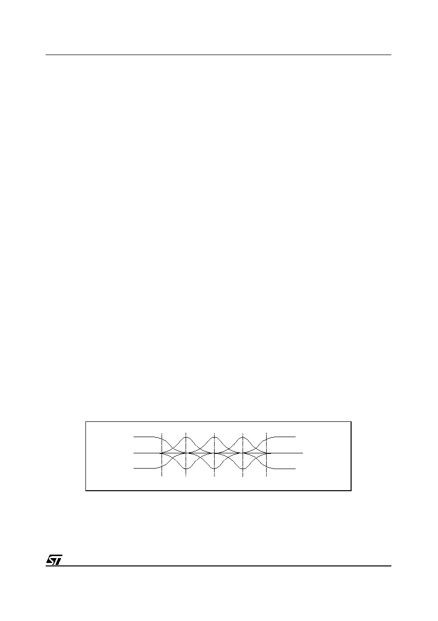
5-Band Audio Equalizer
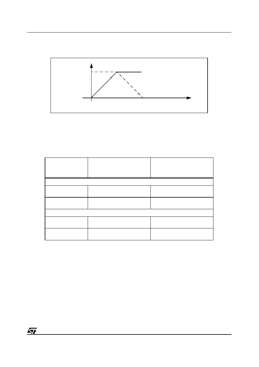
The Loudspeaker audio spectrum is split into 5 frequency bands and the gain of each of them can
be adjusted within a range from -12 dB to +12 dB in steps of 1 dB. The Audio Equalizer may be
used to pre-define frequency band enhancement features dedicated to various kinds of music or to
attenuate frequency resonances of loudspeakers or the listening environment. The Equalizer is
enabled by the EQ_ON bit in the
LS_EQ_CTRL
register. The Bass, Medium and Treble values are
programmed in registers
LS_EQ_BAND[1:5]
.
3.5
Bass/Treble Control
The gain of bass and treble frequency bands for the headphone can be also tuned within a range
from -12 dB to +12 dB in steps of 1 dB. It may be used to pre-define frequency band enhancement
Figure 10: Equalizer
f
1
=100Hz f
2
=330Hz
f
3
=1KHz
f
4
=3.3KHz f
5
=6.6KHz
Audio Processor Block
STV82x6
20/97
features dedicated to various kinds of music, to implement programmable Loudness or Super-bass
functions. The Headphone Bass/Treble feature is enabled by setting the BT_ON bit in the
HP_BT_CTRL
register. The Bass and Treble gain values are adjusted in registers
HP_BASS_GAIN
and
HP_TREBLE_GAIN
, respectively.
3.6
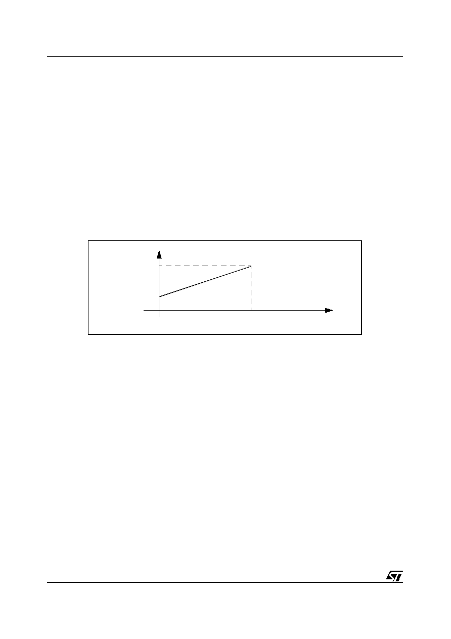
Volume/Balance Control
The STV82x6 provides a Volume/Balance Control for each of the Loudspeaker, Subwoofer and
Headphone audio outputs. Its wide range (from 0 to -96 dB in a linear scale) largely covers typical
home applications (approx. 60 dB) while maintaining a good S/N ratio. Its fine resolution (0.375 dB)
provides simple volume programming and a relative OSD scale representation. The Loudspeaker,
Subwoofer and Headphone volume values should be programmed progressively in steps of less
than 1 dB in order to prevent audible envelope variations and a minimum duration of 16 ms is
required between two successive programming commands to guarantee that there are no audible
plops during volume changes. In this case, a full 8-bit volume scan with minimum steps of 0.375 dB
will last approximately 4 s (minimum).
The Volume/Balance Control can operate in one of two different modes:
In Differential mode (default value), the volume control is a common volume value for both the
Left and Right Loudspeaker and Headphone channels.
In Independent mode, the volume for the Left and Right channels for Loudspeakers or
Headphone is controlled independently.
As the Loudspeaker bass frequencies are output by the Subwoofer, its reference volume is
controlled by default with the value of the
LS_CVOL
common volume register. The
SW_GAIN
register value is used to adjust the level of the Subwoofer output in regards to this reference. In
Independent mode, the
SW_GAIN
register is used as a separated volume control and does not take
into account the Loudspeaker audio level.
3.6.1
Differential Mode
The common value for the Right/Left volume controls for the Loudspeaker, Subwoofer and
Headphone outputs are programmed in registers
LS_CVOL
,
SW_GAIN
and
HP_CVOL
,
respectively. A differential balance can be applied using registers
LS_BAL
and
HP_BAL
to adjust
the Left/Right level ratio as shown in
Figure 12
.
Figure 11: Volume Control
Ou
tpu
t
Ga
in
0 dB
-96 dB
Mute
00h
FFh
I≤C Control
21/97
STV82x6
Audio Processor Block
3.6.2
Independent Mode
This is enabled by setting the BAL_MODE bits in both the
LS_VOL_CTRL
and
HP_VOL_CTRL
registers to Independent mode. In this case, the register values are used to control the volume/
balance functions as described in
Table 6
.
3.6.3
Mute Control
An Independent Mute Control can be used to smooth audio envelope variations in order to prevent
any audible plops can be applied to all audio outputs. This feature is controlled by register
ANA_LS_HP
.
A Headphone Detection Mode that will automatically mute the Loudspeaker and Subwoofer outputs
when a headphone is detected can be enabled by the HDP_ON bit in the
ANA_LS_HP
register. In
this case, only the Headphone output will remain active. See also
Section 3.8: Subwoofer Control
and
Section 5.4: Headphone Detection
.
When a demodulated source is selected on the audio output, the mute is also controlled by
Automatic Standard Recognition system (AUTOSTD). In case of no mono detected or bad detection
of language without backup, the corresponding audio output is automatically muted. In case of
multi-language, the output will be de-muted by selecting an other language with backup.
Figure 12: Differential Balance
Table 6: Volume/Balance Control Registers
Mode
LS_CVOL/LS_VOL_L
HP_CVOL/HP_VOL_L
Register 68h/76h
LS_BAL/LS_VOL_R
HP_BAL/HP_VOL_R
Register 69h/77h
LS_VOL_CTRL (Loudspeaker Volume Control)
BAL_MODE = 0
(Independent Mode)
LS_VOL_L
Left Volume value
LS_VOL_R
Right Volume value
BAL_MODE = 1
(Differential Mode)
LS_CVOL
Common Right/Left Volume value
LS_BAL
Differential Balance value
HP_VOL_CTRL (Headphone Volume Control)
BAL_MODE = 0
(Independent Mode)
HP_VOL_L
Left Volume value
HP_VOL_R
Right Volume value
BAL_MODE = 1
(Differential Mode)
HP_CVOL
Common Right/Left Volume value
HP_BAL
Differential Balance value
Outp
ut Gain
100%
Mute
80h
7Fh
I≤C Control
00h
Right
C
hanne
l
Le
ft C
hannel
Audio Processor Block
STV82x6
22/97
3.7
Automatic Loudness Control
As the human ear does not hear the audio frequency range the same way depending on the power
of the audio source, the Loudness Control corrects this effect by sensing the volume level and then
boosting bass and treble frequencies proportionally to middle frequencies at lower volume.
While maintaining the amplitude of the 1 kHz components at an approximately constant value, the
gain values of lower and higher frequencies are automatically progressively amplified up to +18 dB
when the audio volume level decreases.The maximum treble amplification can be adjusted from
0 dB (first order loudness) to +18 dB (second order loudness). As the volume is proportional to the
external audio amplification power, the loudness amplification threshold is programmable in order to
tune the absolute level. The Loudspeaker Loudness function is enabled by setting the LOUD_ON bit
in register
LS_LOUD
. The Loudness Threshold and Maximum Treble Gain values are also
programmed in this register.
Two bass cut-off frequencies are available:
40 Hz for Normal mode
120 Hz for Bass Amplified mode
The mode is selected by the LOUD_FREQ bit in register
LS_LOUD
(66h).
3.8
Subwoofer Control
The subwoofer signal is created by adding the bass frequency of the Left/Right Loudspeaker
channels. The Subwoofer output is enabled by setting the SW_ON bit in register
ANA_LS_HP
. This
will also force the Headphone output into Mono mode.
The Subwoofer Gain and Frequency Bandwidth values are programmed in registers
SW_GAIN
and
SW_BAND
, respectively. The cut-off frequency can be adjusted from between 50 and 400 Hz in
steps of 50 Hz.
3.9
Beeper
The beeper is used to replace the audio signal with a tone on the Loudspeaker or Headphone
outputs. It can be used for various applications such as beep sounds for remote control, alarm clock
or other features.
Table 7: Headphone/Mute Register Configuration
ANA_LS_HP Register
Output Status
HPD_IN
HPD_ON
SW_ON
MUTE_LS
MUTE_SW
MUTE_HP
Muted
Active
X
0
0
0
X
0
SW
LS, HP Stereo
X
X
1
0
0
1
HP
LS & SW
X
X
X
1
1
1
LS, SW & HP (Channel Change: Mute All)
X
0
1
0
0
0
LS, SW & HP Mono
0
1
0
0
0
0
SW & HP
LS (Default)
1
1
0
0
0
0
SW & LS
HP Stereo
23/97
STV82x6
Audio Processor Block
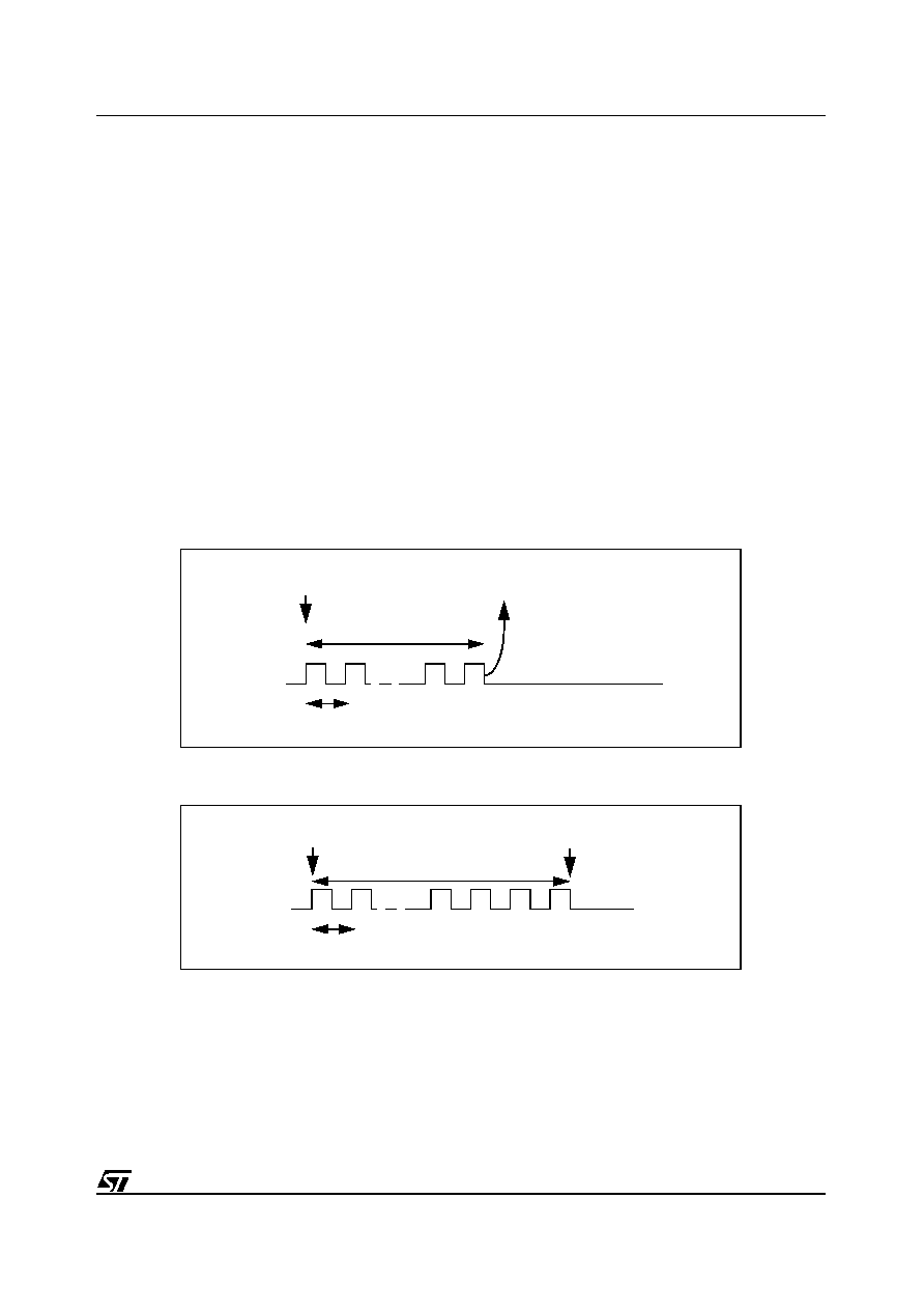
The Beeper operates in one of two modes:
Pulse mode (beep applications) A tone with a programmable short duration (between 128 ms
and 1 s) is generated. Afterwards, the beeper is automatically disabled and the output is
switched back to the audio signal.
Continuous mode (alarm application) A tone with a programmable long duration is generated.
Its start and stop controls must be programmed by I≤C.
In both modes, it is recommended to use the mute function to smooth the audio-to-beeper and
beeper-to-audio (Continuous mode only) transitions. The second transition is automatically muted
in Pulse mode. Beeper parameters are controlled in register
BEEPER_CTRL
.
The beeper tone level and frequency are programmed in register
BEEPER_TONE
. The level (or
volume) ranges between 0 dB and -93 dB in steps of 3 dB and the tone frequency ranges between
62.2 Hz and 8 kHz in steps of 1 octave.
A beep generator is shared only by the Loudspeaker or Headphone outputs. Therefore, in the event
of simultaneous beeps when in Pulse mode, only the first beep will define the effective duration that
will be the same for both outputs.
Note:
The audio output is not affected by the Automatic Mute Control of Automatic Standard Recognition
function when the beeper is activated.
3.10
SRSTM 3D Surround (STV8226/36 only)
In addition to ST WideSurround, the STV8226/36 provides SRSTM 3D Stereo and Mono outputs
which are spatial effects patented by SRS Labs. The SRSTM system is available on the IC when the
SRS_ON bit of register
CUT_ID
is set (STV8226/36 identification). ST and SRSTM Surround
systems cannot be used simultaneously. These signals are output only on the Loudspeaker path.
Figure 13: Pulse Mode
Figure 14: Continuous Mode
0.125s < T < 1s
62.5 Hz < F < 8 kHz
BEEP_ON = 1
BEEP_ON = 0
T predefined
62.5 Hz < F < 8 kHz
BEEP_ON = 1
BEEP_ON = 0
T defined by I≤C write

Audio Processor Block
STV82x6
24/97
SRSTM creates a fully immersed three-dimensional soundfield through the use of a standard
2-speaker stereo configuration. For monaural audio, the source is first converted into a synthetic
stereo signal before creating the 3D effect. The virtual gain for the Surround and Center
components can be adjusted by registers
LS_SRS_SPACE
and
LS_SRS_CENTER
(respectively)
in Stereo mode only. These values are used to adapt spatial effects to the source.
For ST WideSurround Sound, Stereo or Mono output mode is automatically selected by the
Automatic Standard Recognition System (AUTOSTD) according to the detected audio source. By
default, ST WideSurround Sound is selected. SRSTM Surround is selected in register
LS_SRD_CTRL
.
25/97
STV82x6 Audio
Matrices
4
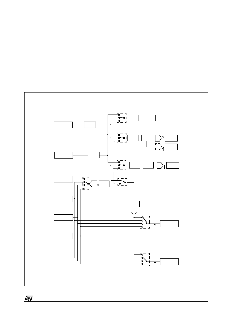
Audio Matrices
In addition to the sound carrier source (SIF), the STV82x6 accepts up to three analog stereo audio
inputs (2 V
RMS
SCART compatible) and one analog mono audio input (0.5 V
RMS
). These different
sources can go back out through four analog stereo audio outputs which are Loudspeaker +
Subwoofer and Headphone (1 V
RMS
) and two compatible SCART audio outputs (2 V
RMS
). An extra
digital stereo output (I≤S compatible) is available for interfacing with a Dolby Pro Logic Decoder or
an external Digital-to-Analog Converter (DAC).
Figure 15: Audio Matrix Block Diagram
SCART1 In
SCART2 In
SCART3 In
Mono In
I≤S
LS
SCART1 Out
SCART2 Out
A/D
D/A
Lang.
Select
CH_SEL (49h)
Low Noise
Mute
SW1
SW2
SW3
SW4
SW6
SW7
D/A
Low Noise
Mute
SW5
D/A
SW
Low Noise
Low Noise
Switch
Demodulator
Level
Prescaling
CH_LANG (4Ah)
CH_SEL (49h)
CH_LANG (4Ah)
CH_SEL (49h)
CH_LANG (4Ah)
CH_SEL (49h)
CH_LANG (4Ah)
ANA_SCART (06h)
ANA_SCART (06h)
ANA_SCART (06h)
CH_MX (48h)
Demod.
Matrix
CH_MX (48h)
SIF
MONOIN
(AI1L, AI1R)
(AI2L, AI2R)
(AI3L, AI3R)
(AO1L, AO1R)
(AO2L, AO2R)
SDO
(LSL, LSR)
SW
(HPL, HPR)
Lang.
Select
Audio
DSP
HP
D/A
Lang.
Select
Audio
DSP
Low Noise
Mute
Lang.
Select
SCART
Matrix
Low Noise
Mute
Switch
Low Noise
Low Noise
Mute
Switch
I≤S
I≤S
Matrix
CH_MX (48h)
SDI

Audio Matrices
STV82x6
26/97
4.1
Input Audio Matrix
The mono input (MONOIN) and three stereo SCART inputs (AI1L, AIR1), (AI2L, AI2R) and (AI3L,
AI3R) can be switched to any audio output and the same source can be connected to different
outputs. The inputs can totally bypass the STV82x6 functions (Thru mode) via the full analog
SCART path or use the audio processing corresponding to the different audio outputs. The input
matrix is programmed in bits DSP_ISCART_SEL[1:0] of register
ANA_SCART
.
In Thru mode, the STV82x6 is switched into Low Power mode (Standby) and the audio matrix
configuration (ANA_SCART register) is memorized and is not reset when switched back to Full
Power mode. See
Section 7.2: Standby Mode
.
Before processing the audio signal, the selected analog input is converted into a digital 16-bit signal
and pre-processed. Its sound level can be prescaled within a range between -6 dB and +6 dB in
steps of 1 dB (register
PRE_AUX
) and for Left/Right channels (register
CH_MX
). The internal level
can be measured with the Peak Level Detector.
4.2
Output Audio Matrix
The Loudspeaker+Subwoofer (LSL, LSR, SW), Headphone (HPL, HPR) and I≤S (SDO) outputs can
directly select two possible sources which are either the demodulated signal or the converted audio
input (from the SCART or mono input) in register
CH_SEL
. In the event of a dual mono source, the
language is selected in register
CH_LANG
.
The two analog SCART outputs (AO1L, AO1R) and (AO2L, AO2R) can be used to bypass the
STV82x6 functions by directly selecting the analog input SCARTs or the output digital source from
the demodulator or the converted audio input (with prescaling and Left/Right re-matrixing). The
SCART output is selected in register
ANA_SCART
and the digital source in register
CH_SEL
. In the
event of a dual mono source, the language is selected in register
CH_LANG
as other audio outputs.
In the event of a demodulator source selection, the mute is automatically controlled for all audio
outputs.

27/97
STV82x6
Additional Controls and Flags
5
Additional Controls and Flags
5.1
Interrupt Request
The identified TV sound standard is displayed in register
AUTO_STAT
. Each change in the detected
standard is flagged to the host system via hardware pin IRQ. The flag must be reset by re-
programming the IRQ bit in register
AUTO_CTRL
and then checking the detected standard status
by reading registers AUTO_STAT, NICAM_STAT, ZWT_STAT and CH_MX.
5.2
I≤C Bus Expander
Pins BUS0 and BUS1 can be used to control external switchable IF SAW filters or audio switches.
These pins can be directly programmed by register
CTRL
.
5.3
Stereo Flag
For Loudspeakers only, a Stereo Mode Detection flag (the ST_ID bit in register
AUTO_STAT
) is set
when a demodulated source is selected and a stereo standard is detected. The stereo flag is also
output on pin ST in order to control an external indicator (e.g. LED). The stereo mode is also
displayed by status register
AUTO_STAT
.
CAUTION: When the I≤S input is selected, the stereo flag is no longer available on pin ST.
5.4
Headphone Detection
For the headphone, the HPD input can be used to automatically mute the Loudspeaker and
Subwoofer outputs when the HPD_ON bit is set in register
ANA_LS_HP
(active low). The HPD pin
must be set for the mute function to be active.
Figure 16: Headphone Detection
A
u
dio Matrix
Mute Control
Headphone
Left
Right
Sub-
I≤C Control
STV82x6
Loudspeaker
Audio Processing
Headphone
Audio Processing
Subwoofer
Audio Processing
woofer
Detection

I≤S Interface
STV82x6
28/97
6
I≤S Interface
A digital stereo input is available for a virtual Dolby source from an external decoder.
A digital stereo output (I≤S compatible) is available for routing the demodulated signal or a converted
input audio signal into a Dolby Pro Logic Decoder or an external DAC. The STV82x6 I≤S interface
drives the serial bus (SCK, WS, SDO) in Master mode in format 32.fs with a sampling frequency (f
S
)
of 32 kHz. An additional master clock (MCK) in format 256.fs (f
S
= 8.192 MHz) is provided if
required for the slave interface.
Both Philips and Sony modes are supported with programmable Word Selection (WS) polarity
(register
I2S
). By default, all I≤S digital outputs are set in high impedance and must be switched to
low impedance via register
CTRL
before use.
A clock system output (SYSCK) is also available for clock peripherals using the same quartz
frequency as the STV82x6. By default, this clock output (identical to the crystal oscillator) is set to
high impedance and must be switched to low impedance via register
CTRL
before use.
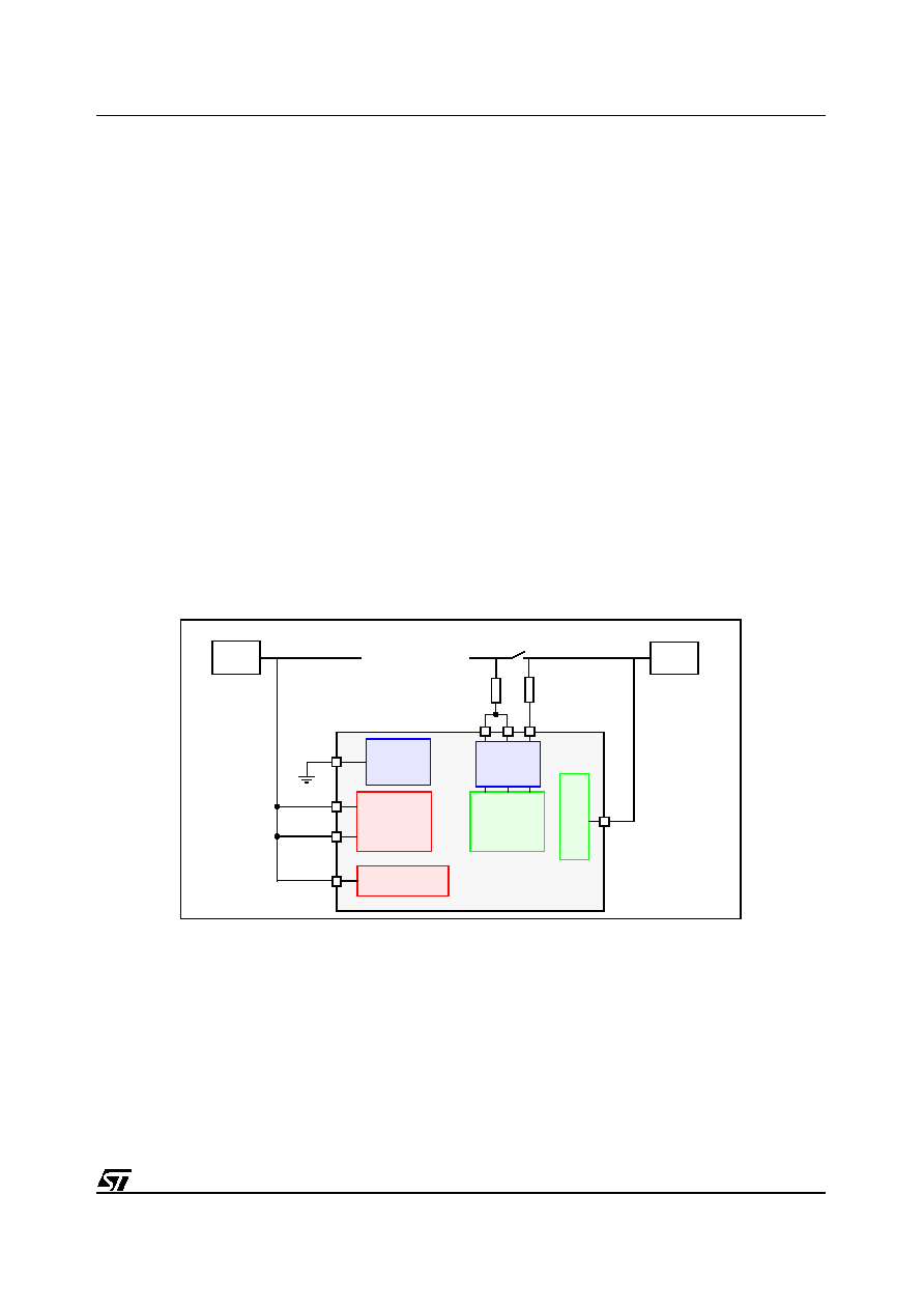
29/97
STV82x6 Power
Supplies
7
Power Supplies
7.1
Supply Voltages
The STV82x6 supports different power configurations due to its integrated voltage regulators.
Typically, two power supplies, which are grouped into two sets of IC pins, are required.
1. Digital Power Supply (DPS) This supply may be either 3.3 V or 5 V if an external power
transistor is used. The DPS supplies pins VDD1, VDD2 and VDDP.
-- In 3.3 V mode, the power is directly supplied to the digital power pins. In this case, the REG
pin is not used and must be connected to the ground.
-- 5 V mode requires the use of an external transistor coupled to the integrated voltage
regulator via the REG pin in order to generate a stable 3.3 V supply to the digital power pins.
2. Analog Power Supply (APS) This supply may be either 8 V or 5 V. In both cases, external
resistors are required, except for pin VDDH. The APS supplies pins VDDIF, VDDC, VDDA and
VDDH.
-- The 8 V power supply is directly connected to pin VDDH and offers a 2 V
RMS
dynamic
voltage on SCART outputs. The other analog power pins can be supplied with an 8 V or 5 V
supply through external resistors.
-- If only a 5 V power supply is available for pin VDDH, the SCART outputs will be reduced to
1 V
RMS
. In this case, the SEL5V bit must be set in register
ANA_CTRL
.
Figure 17: 3.3 V / 8 V or 3.3 V / 5 V Application
3.3 V
Regulator
Digital Core
Clock Generator
Au
dio
Bu
f
f
er
Analog
REG
VDDH
STV82x6
3.3 V
DPS
Standby
VDD1
VDD2
VDDP
VDDI
F
VDDC
VDDA
8 or 5 V
APS
Core
Digital
3.3 V
Regulator
Analog
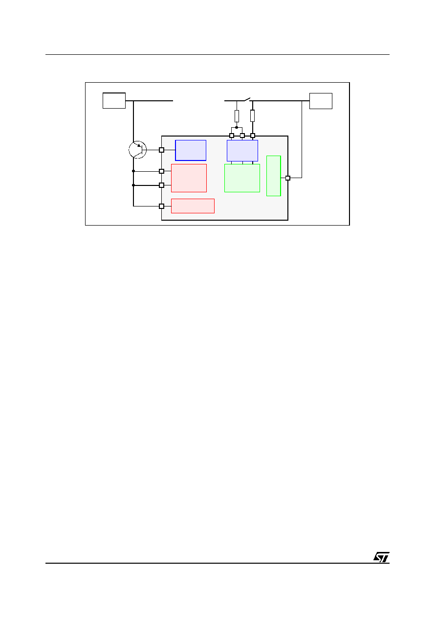
Power Supplies
STV82x6
30/97
7.2
Standby Mode
The STV82x6 provides a Thru mode configuration that bypasses IC functions via a SCART I/O pin
(Full Analog Path only). In this case, only minimum power is required (Standby mode).
In Standby mode, the digital and analog power supplies are switched off, except for pins VDDA and
VDDH which are used to maintain the SCART path, the last configuration programmed for analog
matrixing (register
ANA_SCART
) and the power configuration (register
ANA_CTRL
). When
switching back to normal Full Power mode, all I≤C registers are reset except for those used in
Standby mode to maintain the original configuration.
In Standby mode, the I≤C bus does not operate. However, the bus can still be used by other ICs
since the I≤C I/O pins (SDA and SCL) of the STV82x6 are forced into a high-impedance
configuration.
Figure 18: 5 V / 8 V or 5 V / 5 V Application
Digital Core
Clock Generator
Au
dio
Bu
f
f
er
Analog
REG
VDDH
STV82x6
5 V
DPS
Standby
VDD1
VDD2
VDDP
VDDI
F
VDDC
VDDA
8 or 5 V
APS
Core
3.3 V
Regulator
Analog
3.3 V
Regulator
Digital
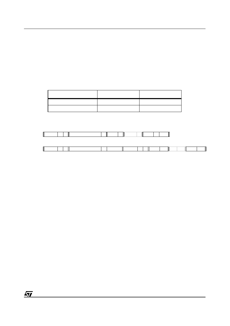
31/97
STV82x6
I≤C Bus
8
I≤C Bus
8.1
I≤C Address and Protocol
The STV82x6 I≤C interface works in Slave mode and is fully compliant with I≤C standards in Fast
mode (maximum frequency of 400 kHz). Two pairs of I≤C chip addresses are used to connect two
STV82x6 chips to the same I≤C serial bus. The device address pairs are defined by the polarity of
the ADR pin and are listed in the following table:
Protocol Description
Write Protocol
Read Protocol
W = Write address,
R = Read address,
A = Acknowledge,
N = No acknowledge.
Sub-address is the register address pointer; this value auto-increments for both write and read.
The STV82x6 cannot immediately reply to an I≤C read request when addressing DSP registers
(addresses 40h and greater).The I≤C interface holds the I≤C Serial Clock (SCL) line low before each
data byte is read to compensate for the latency of the DSP response (64 µs in worst case). The
implemented I≤C Pulling Down mode is compatible with a Continuous or Stopped SCL when held
low (restart at high level, if stopped) and operates between 24 kHz and 400 kHz. If SCL Pulling
Down mode is not supported by the Master I≤C interface, the Pulling Down system can be de-
activated by setting the SCLPD_OFF bit in register
RESET
. In this case, two successive reads of
the same DSP register are required and only the second one is valid (first read is `don't care'). This
special protocol is no longer compatible with the I≤C sub-address auto-incrementation function in
Read mode.
8.2
STV82x6 Reset
All STV82x6 features are controlled via the I≤C bus. However, the device is designed to power up
into a fully working default mode without having to be sent I≤C bus data to set it up.
The STV82x6 can be "reset" in 2 ways:
1. By Software via the I≤C bus: This clears all synchronous logic, except for the I≤C bus registers.
2. By Hardware via the RESET pin: In addition to clearing all synchronous logic, the RESET input
(active low) resets all the I≤C bus registers to the default values listed below.
Table 8: I≤C Read/Write Addresses
ADR
Write address (hex) (W)
Read address (hex) (R)
LOW (connected to GND1)
80h
81h
HIGH (connected to VDD1)
A0h
A1h
Start
W
A
Sub-address
A
Data
A
....
A
Data
A
Stop
Start
W
A
Sub-address
A
Stop
Start
R
A
Data
A
....
A
Data
N
I≤C Bus
STV82x6
32/97
Table 9: RESET Default Values
Function
Default mode
Demodulation
Auto-standard
ON
Scanned Standards
M/N, B/G, I, L/L'
FM Deviation
± 125 kHz (Max.)
Audio Outputs
Automatic Mute Mode
ON
Loudspeaker Source
Demodulated Sound
Loudspeaker Volume
-48 dB / muted
Loudspeaker L/R Balance
L/R = 100%
Subwoofer
-48 dB / OFF
Headphone Source
Demodulated Sound
Headphone Automatic Detection
ON
Headphone Volume
-48 dB / Muted
Headphone L/R Balance
L/R = 100%
SCART-1 out
Demodulated Sound
SCART-2 out
SCART1 Source
I≤S out
OFF
Audio Processing
Loudspeaker/Headphone SVC
OFF, 0 dB Reference Value
Loudspeaker Surround
OFF
Loudspeaker 5-Band Equalizer
OFF, 0 dB (Flat Band)
Loudspeaker Loudness
OFF
Headphone Bass/Treble
OFF, 0 dB (Flat Band)
Loudspeaker/Headphone Beeper
-48 dB / OFF
33/97
STV82x6
Register List
9
Register List
Note:
The unused bits (defined as reserved) in I≤C registers must be kept to zero.
The system clock registers (from address 08h to 0Bh) do not need to be modified if a standard
27 MHz quartz crystal is used
The demodulator registers (from address 0Ch to 54h) default values are optimum and any change
is not recommended, except for:
AGCS (0Fh) to adjust AGC gain for AM carrier in L/L' standard (AGC used in open loop)
CAROFFSET1(22h) and CAROFFSET2(3Ah) to compensate IF carrier frequency with an out-
of-standard offset
Soundlevel Prescaling PRE_FM(44h), PRE_NICAM(45h) and PRE_AUX(46h) to equalize
demodulated or external audio signal before audio processing. Peak detector registers
PEAK_DET_CTRL(4Bh) and PEAK_DET_STAT(4Ch) can be used to measure internal sound
level.
Sound source selection for each audio output channel Loudspeaker+Subwoofer, Headphone,
SCART and I≤S to be done using CH_SEL(49h)
In Multi-lingual mode, CH_LANG(4Ah) selects separately the language for each audio output
channel.
AUTO_CTRL(50h) to select between L/L' or D/K/K1/K2/K3 standard which can be
discriminated automatically. To be used also to change maximum FM deviation (125 kHz, by
default) in case of wide overmodulation.
AUTO_SCKM(51h) and AUTO_SCKST(52h) to define the list of mono and stereo standards to
be recognized automatically.
Note:
() used in reset value column means that the bit or the byte is read-only.
(S) symbol indicates that the field value is represented in signed binary format.
(*) The field AGC_ERR[4:0] (AGCS) can be written by user if the bit AGC_CMD (AGCC) is set to
one (by default controlled by AUTOSTD). To be used to adjust manually the input gain of analog
AGC amplifier for AM carrier (L/L').
9.1
I≤C Register Map
By default, all I≤C registers controlled by Automatic Standard Recognition System (AUTOSTD) are
forced to Read-only mode for the user. These registers and bits are shaded in
Table 10
.
Table 10: List of I≤C Registers (Sheet 1 of 5)
Name
Addr.
(Hex)
Reset
Value (Bin)
Register Function and Description
Bit 7
Bit 6
Bit 5
Bit 4
Bit 3
Bit 2
Bit 1
Bit 0
IC General Control
CUT_ID
00h
(0001 0001)
SRS_ON
0
CUT_NUMBER[5:0]
RESET
02h
0000 0000
0
SCLPD_OF
F
AUTO_OFF
0
0
SOFT_LRS
T1
SOFT_LRS
T2
SOFT_RST
CTRL
03h
0000 0000
0
BUS_EXPAND[1:0]
I≤S_EN
SDI_EN
0
MCK_EN
SYSCK_EN
I2S
04h
0000 0000
0
0
0
0
I2S_STD
I2S_WSPO
L
0
0
Register List
STV82x6
34/97
Audio Mute & Switch
ANA_CTRL
05h
0000 0000
SEL5V
0
0
0
0
0
0
0
ANA_SCART
06h
0010 1100
DSP_ISCART_SEL[1:0]
MUTE_OSC
ART2
OSCART2_SEL[1:0]
MUTE_OSC
ART1
OSCART1_SEL[1:0]
ANA_LS_HP
07h
(0)100 0111
HPD_IN
HPD_ON
SW_ON
0
0
MUTE_LS
MUTE_SW
MUTE_HP
Clocking
PLL_DIV
08h
0000 0101
0
0
SDIV[2:0]
FDIV[2:0]
PLL_MD
09h
0001 1110
0
0
0
MD2[4:0]
PLL_PEH
0Ah
0000 0001
0
0
0
0
PE1[11:8]
PLL_PEL
0Bh
1110 1000
PE1[7:0]
Demodulator
DEMOD_CTRL
0Ch
0000 0110
0
0
0
0
AM_SEL
DEMOD_MODE[2:0]
DEMOD_STAT
0Dh
(0000 0000)
0
0
0
QPSK_LK
FM2_CAR
FM2_SQ
FM1_CAR
FM1_SQ
AGCC
0Eh
0001 0001
AGC_ CMD
0
0
AGC_REF[2:0]
AGC_CST[1:0]
AGCS
0Fh
(0000 0000)
0
AGC_ERR[4:0] (*)
SIG_OVER
SIG_UNDE
R
DCS
10h
(0000 0000)
DC_ERR[7:0]
Demodulator Channel 1
CARFQ1H
12h
0011 1110
CARFQ1[23:16]
CARFQ1M
13h
1000 0000
CARFQ1[15:8]
CARFQ1L
14h
0000 0000
CARFQ1[7:0]
FIR1C0
15h
0000 0000
FIR1C0[7:0] (S)
FIR1C1
16h
1111 1110
FIR1C1[7:0] (S)
FIR1C2
17h
1111 1100
FIR1C2[7:0] (S)
FIR1C3
18h
1111 1101
FIR1C3[7:0] (S)
FIR1C4
19h
0000 0010
FIR1C4[7:0] (S)
FIR1C5
1Ah
0000 1101
FIR1C5[7:0] (S)
FIR1C6
1Bh
0001 1000
FIR1C6[7:0]6 (S)
FIR1C7
1Ch
0001 1111
FIR1C7[7:0] (S)
ACOEFF1
1Dh
0010 0011
ACOEFF1[7:0]
BCOEFF1
1Eh
0001 0010
BCOEFF1[7:0]
CRF1
1Fh
(0000 0000)
CRF[7:0] (S)
CETH1
20h
0010 0000
CETH1[7:0]
SQTH1
21h
0011 1100
SQTH1[7:0]
CAROFFSET1
22h
0000 0000
CAROFFSET1[7:0] (S)
Demodulator Channel 2
IAGCR
25h
1000 1000
IAGC_REF[7:0]
IAGCC
26h
0000 0011
IAGC_ OFF
0
0
0
0
IAGC_CST[2:0]
Table 10: List of I≤C Registers (Sheet 2 of 5)
Name
Addr.
(Hex)
Reset
Value (Bin)
Register Function and Description
Bit 7
Bit 6
Bit 5
Bit 4
Bit 3
Bit 2
Bit 1
Bit 0
35/97
STV82x6
Register List
IAGCS
27h
(0000 0000)
IAGC_CTRL[7:0]
CARFQ2H
28h
0100 0100
CARFQ2[23:16]
CARFQ2M
29h
0100 0000
CARFQ2[15.8]
CARFQ2L
2Ah
0000 0000
CARFQ2[7:0]
FIR2C0
2Bh
0000 0000
FIR2C0[7:0] (S)
FIR2C1
2Ch
0000 0000
FIR2C1[7:0] (S)
FIR2C2
2Dh
0000 0000
FIR2C2[7:0] (S)
FIR2C3
2Eh
0000 0000
FIR2C3[7:0] (S)
FIR2C4
2Fh
1111 1111
FIR2C4[7:0] (S)
FIR2C5
30h
0000 0100
FIR2C5[7:0] (S)
FIR2C6
31h
0001 0100
FIR2C6[7:0] (S)
FIR2C7
32h
0010 0101
FIR2C7[7:0] (S)
ACOEFF2
33h
1001 0000
ACOEFF2[7:0]
BCOEFF2
34h
1010 1100
BCOEFF2[7:0]
SCOEFF
35h
0001 1100
SCOEFF[7:0]
SRF
36h
(0000 0000)
SRF[7:0] (S)
CRF2
37h
(0000 0000)
CRF2[7:0] (S)
CETH2
38h
0010 0000
CETH2[7:0]
SQTH2
39h
0011 1100
SQTH2[7:0]
CAROFFSET2
3Ah
0000 0000
CAROFFSET2[7:0] (S)
NICAM
NICAM_CTRL
3Dh
0000 0000
0
0
0
0
0
DIF_POL
ECT
MAE
NICAM_BER
3Eh
(0000 0000)
ERROR[7:0]
NICAM_STAT
3Fh
(0000 0000)
NIC_DET
F_MUTE
LOA
CBI[4:1]
NIC_MUTE
Stereo FM
ZWT_CTRL
40h
0011 0001
0
STD_MODE
THRESH[3:0]
TSCTRL[1:0]
ZWT_STAT
41h
(0000 0000)
0
0
0
0
0
ZW_DET
ZW_ST
ZW_DM
Sound Preprocessing & Selection
FM_DCL
42h
(0000 0000)
FM_DCL[7:0] (S)
FM_DCR
43h
(0000 0000)
FM_DCR[7:0] (S)
PRE_FM
44h
0000 0110
0
0
FM_PRESCALE[5:0] (S)
PRE_NICAM
45h
0000 1101
0
0
NICAM_PRESCALE[5:0] (S)
PRE_AUX
46h
0000 0000
I2S_PRESCALE[3:0] (S)
SCART_PRESCALE[3:0] (S)
CH_CTRL
47h
0000 0000
MUTE_D01
2
MUTE_D12
NIC_DMX
NICDPH_O
FF
FM_DMX[1:0]
FMDPH_OF
F
FMDPH_S
W
CH_MX
48h
0000 0000
I2S_MX[1:0]
SC_MX[1:0]
DEMOD_MX[3:0]
CH_SEL
49h
0000 0000
I2S_SEL[1:0]
SC_SEL[1:0]
HP_SEL[1:0]
LS_SEL[1:0]
CH_LANG
4Ah
0000 0000
I2S_LANG[1:0]
SC_LANG[1:0]
HP_LANG[1:0]
LS_LANG[1:0]
Table 10: List of I≤C Registers (Sheet 3 of 5)
Name
Addr.
(Hex)
Reset
Value (Bin)
Register Function and Description
Bit 7
Bit 6
Bit 5
Bit 4
Bit 3
Bit 2
Bit 1
Bit 0
Register List
STV82x6
36/97
PEAK_DET_CTRL
4Bh
0000 0000
0
0
0
0
0
0
PD_SEL[1:0]
PEAK_DET_STATL
4Ch
(0000 0000)
PEAK_LEVEL_LEFT[7:0]
PEAK_DET_STATR
4Dh
(0000 0000)
PEAK_LEVEL_RIGHT[7:0]
Automatic Standard Recognition System
AUTO_CTRL
50h
0000 0001
0
0
0
IRQ
SINGLE_SH
OT
DK_DEV[1:0]
LDK_SW
AUTO_SCKM
51h
0000 1111
0
0
0
0
LDK_SCK
I_SCK
BG_SCK
MN_SCK
AUTO_SCKST
52h
0001 1111
LDK_ZWT3
LDK_ZWT2
LDK_SWT1
LDK_NIC
I_NIC
BG_ZWT
BG_NIC
MN_ZWT
AUTO_TIMER
53h
1010 0100
FM_TIME[1:0]
NICAM_TIME[2:0]
ZWEITON_TIME[2:0]
AUTO_STAT
54h
0(000 0000)
ST_ID
STEREO_S
TATE
MONO_STA
TE
AUTO_ON
STEREO_SID[1:0]
MONO_SID[1:0]
Audio Processing
SVC_SEL
59h
0000 0000
0
0
0
0
0
0
0
SVC_SW
SVC_CTRL
5Ah
0000 0000
SVC_ON
SVC_TIME[1:0]
SVC_REF[4:0] (S)
LS_SRD_CTRL
5Bh
0000 0000
SRD_ON
0
0
0
0
SRD_SEL
SRD_STER
EO
STS_MODE
LS_STS_GAIN
5Ch
1000 0000
ST_GAIN[7:0]
LS_STS_FREQ
5Dh
00010101
0
0
BASS_FREQ[1:0]
MEDIUM_FREQ[1:0]
TREBLE_FREQ[1:0]
LS_SRS_SPACE
5Eh
1000 0000
SRS_SPACE[7:0] (for Stereo mode only)
LS_SRS_CENTER
5Fh
1000 0000
SRS_CENTER[7:0] (for Stereo mode only)
LS_EQ_CTRL
60h
0000 0000
EQ_ON
0
0
0
0
0
0
R
LS_EQ_BAND1
61h
0000 0000
0
0
0
EQ_BAND1_GAIN[4:0] (S)
LS_EQ_BAND2
62h
0000 0000
0
0
0
EQ_BAND2_GAIN[4:0] (S)
LS_EQ_BAND3
63h
0000 0000
0
0
0
EQ_BAND3_GAIN[4:0] (S)
LS_EQ_BAND4
64h
0000 0000
0
0
0
EQ_BAND4_GAIN[4:0] (S)
LS_EQ_BAND5
65h
0000 0000
0
0
0
EQ_BAND5_GAIN[4:0] (S)
LS_LOUD
66h
0000 0010
LOUD_TH_
ON
LOUD_TH[2:0]
LOUD_
FREQ
LOUD_TH_GHR[2:0]
LS_VOL_CTRL
67h
0000 0001
0
0
0
0
0
0
0
BAL_MODE
LS_CVOL
/
LS_VOL_L
68h
1000 0000
CVOL[7:0]
LS_BAL
/
LS_VOL_R
69h
0000 0000
BAL[7:0] (S)
SW_GAIN
6Ah
1000 0000
SW_GAIN[5:0]
SW_BAND
6Bh
0000 0011
0
0
0
0
0
SW_FREQ[2:0]
Headphone Channel
HP_BT_CTRL
71h
0000 0000
BT__ON
0
0
0
0
0
0
0
HP_BASS_GAIN
72h
0000 0000
0
0
0
BASS_GAIN[4:0] (S)
HP_TREBLE_GAIN
73h
0000 0000
0
0
0
TREBLE_GAIN[4:0] (S)
HP_VOL_CTRL
75h
0000 0001
BAL_MODE
Table 10: List of I≤C Registers (Sheet 4 of 5)
Name
Addr.
(Hex)
Reset
Value (Bin)
Register Function and Description
Bit 7
Bit 6
Bit 5
Bit 4
Bit 3
Bit 2
Bit 1
Bit 0
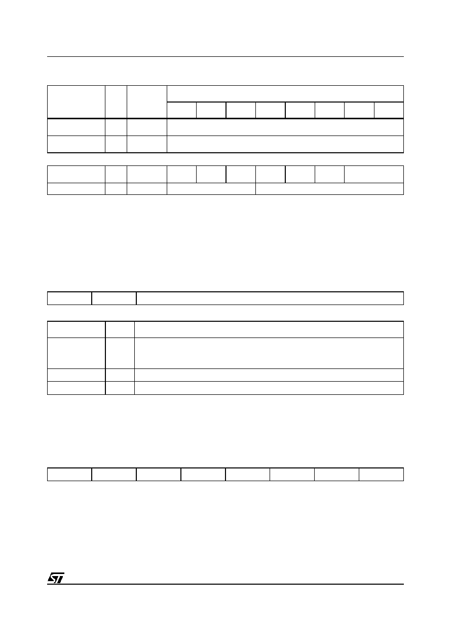
37/97
STV82x6
Register List
9.2
STV82x6 General Control Registers
CUT_ID Version
Identification
RESET
Software Reset Register
Description
The built-in Automatic Standard Recognition System (AUTOSTD) can be disabled by bit
AUTO_OFF (when high). In this case, the Software Reset function (bits SOFT_LRESTART1 and
SOFT_LRESTART2) can be used to implement the Automatic Standard Recognition by I≤C
Software. This is not required if the built-in Automatic Standard Recognition System function is used
(default).
HP_CVOL
/
HP_VOL_L
76h
1000 0000
CVOL[7:0]
HP_BAL
/
HP_VOL_R
77h
0000 0000
BAL[7:0] (S)
Beeper
BEEPER_CTRL
79h
0000 0000
LS_BEEP_
ON
HP_BEEP_
ON
BEEP_MOD
E
0
0
0
BEEP_DURATION[1:0]
BEEPER_TONE
7Ah
0111 0000
BEEP_FREQ[2:0]
BEEP_VOL[4:0]
Address (hex): 00h
Type: R
Bit 7
Bit 6
Bit 5
Bit 4
Bit 3
Bit 2
Bit 1
Bit 0
SRS_ON
0
CUT_NUMBER[5:0]
Bit Name
Reset
Function
SRS_ON
0
Identifies the STV82x6 version
0: version without SRSTM (STV82x6) - Only ST WideSurround can be used
1: version with SRSTM (STV8226/36) - Both SRSTM and ST WideSurround are available
Bit 6
0
Reserved.
CUT_NUMBER[5:0]
010001 Dice Version Identification
Address (hex): 02h
Type: R/W
Bit 7
Bit 6
Bit 5
Bit 4
Bit 3
Bit 2
Bit 1
Bit 0
0
SCLPD_OFF
AUTO_OFF
0
0
SOFT_LRST1 SOFT_LRST2
SOFT_RST
Table 10: List of I≤C Registers (Sheet 5 of 5)
Name
Addr.
(Hex)
Reset
Value (Bin)
Register Function and Description
Bit 7
Bit 6
Bit 5
Bit 4
Bit 3
Bit 2
Bit 1
Bit 0
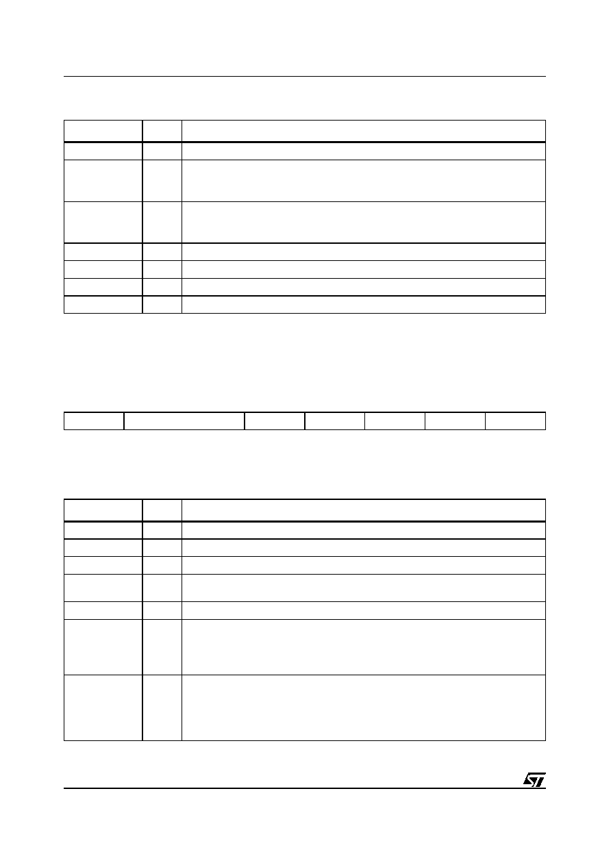
Register List
STV82x6
38/97
CTRL
Hardware Interface Control Register
Description
Provides all hardware controls to drive external components (SAW Filter, Audio Switches) and
additional Audio Decoder (Dolby Pro Logic) via register
I2S
including the Master and Quartz Clocks.
Bit Name
Reset
Function
Bit7
0
Reserved.
SCLPD_OFF
SCL Pulling-down System Disable
0: System is enabled
1: System is disabled
AUTO_OFF
0
Automatic Standard Recognition System Disable
0: System is enabled
1: System is disabled
Bits[4:3]
00
Reserved.
SOFT_LRESTART1
0
Softreset (active high) of Channel 1 detectors only.
SOFT_LRESTART2
0
Softreset (active high) of Channel 2 detectors only.
SOFTRST
0
General softreset (active high) to reset all hardware registers except for I≤C data.
Address (hex): 03h
Type: R/W
Bit 7
Bit 6
Bit 5
Bit 4
Bit 3
Bit 2
Bit 1
Bit 0
0
BUS_EXPAND[1:0]
I2S_EN
SDI_EN
0
MCK_EN
SYSCK_EN
Bit Name
Reset
Function
Bit 7
0
Reserved.
BUS_EXPAND[1:0]
00
Static control by I≤C of hardware pins BUS1 and BUS0.
I2S_EN
0
When 1, the I≤S hardware pin is enabled (SCK, WS, SDO)
SDI_EN
0
When 1, the SDI input pin is enabled (switch with ST output). Must be used when I≤S mode is
selected.
Bit 2
0
Reserved.
MCK_EN
0
Master Clock Enable
Enables the master clock output (256.fs) to interface by I≤S with the Dolby Pro Logic Decoder.
0: Disabled.
1: Enabled
SYSCK-EN
0
System Clock Enable
Enables the system clock output to provide the quartz clock required to interface with the Dolby Pro
Logic Decoder.
0: Disabled.
1: Enabled
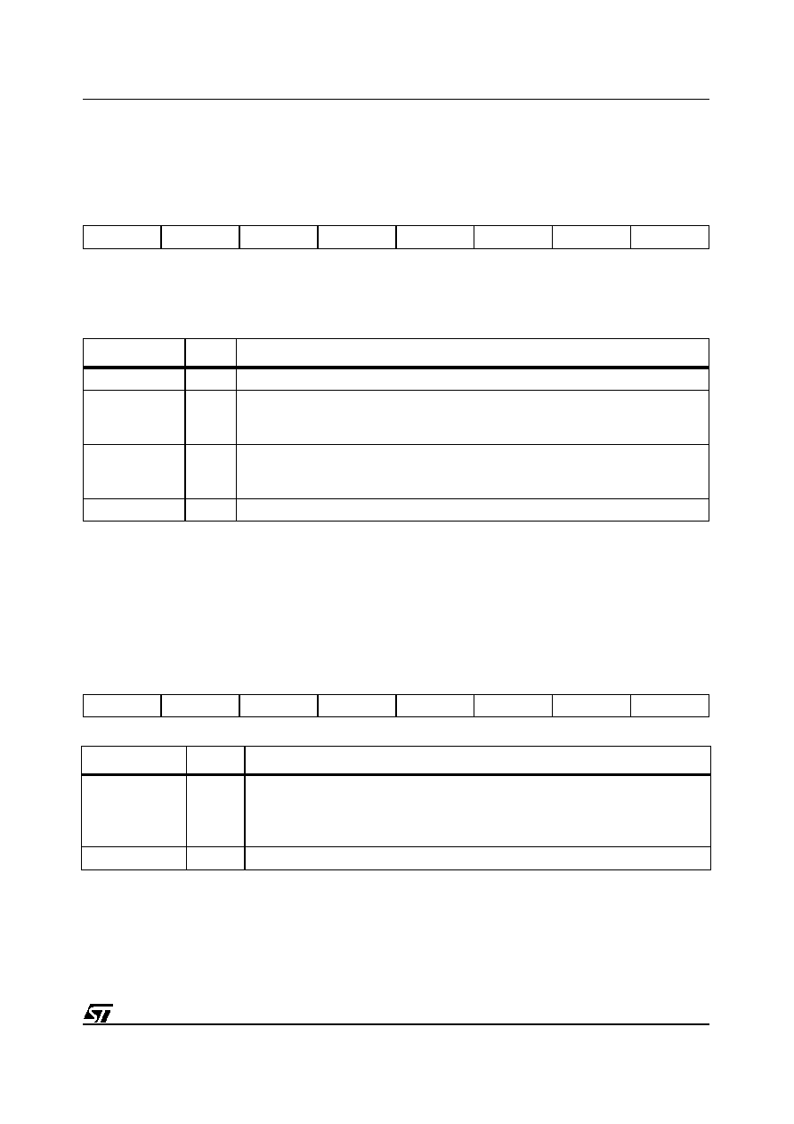
39/97
STV82x6
Register List
I2S
I≤S Interface Control Register
Description
Proposes most used I≤S standard (Philips and Sony) with Word Select (WS) polarity programming.
Only Master mode is supported. All interfaced chip must be set in slave mode.
9.3
Analog Block
ANA_CTRL
Power Supply Configuration Control Register
Address (hex): 04h
Type: R/W
Bit 7
Bit 6
Bit 5
Bit 4
Bit 3
Bit 2
Bit 1
Bit 0
0
0
0
0
I2S_STD
I2S_WSPOL
0
0
Bit Name
Reset
Function
Bits[7:4]
0000
Reserved.
I2S_STD
0
I≤S Standard Select
0: Philips Standard (Default)
1: Sony Standard
I2S_WSPOL
0
I≤S Word Select Polarity Select
0: No WS inversion (Default)
1: WS with polarity inversion
Bits[1:0]
00
Reserved.
Address (hex): 05h
Type: R/W
Bit 7
Bit 6
Bit 5
Bit 4
Bit 3
Bit 2
Bit 1
Bit 0
SEL5V
0
0
0
0
0
0
0
Bit Name
Reset
Function
SEL5V
0
5 V Analog Power Supply Select
The audio power amplifiers should be muted before changing this bit.
0: 8 V Analog Power Supply (Default).
1: 5 V Analog Power Supply
Bit[6:0]
0000000
Reserved
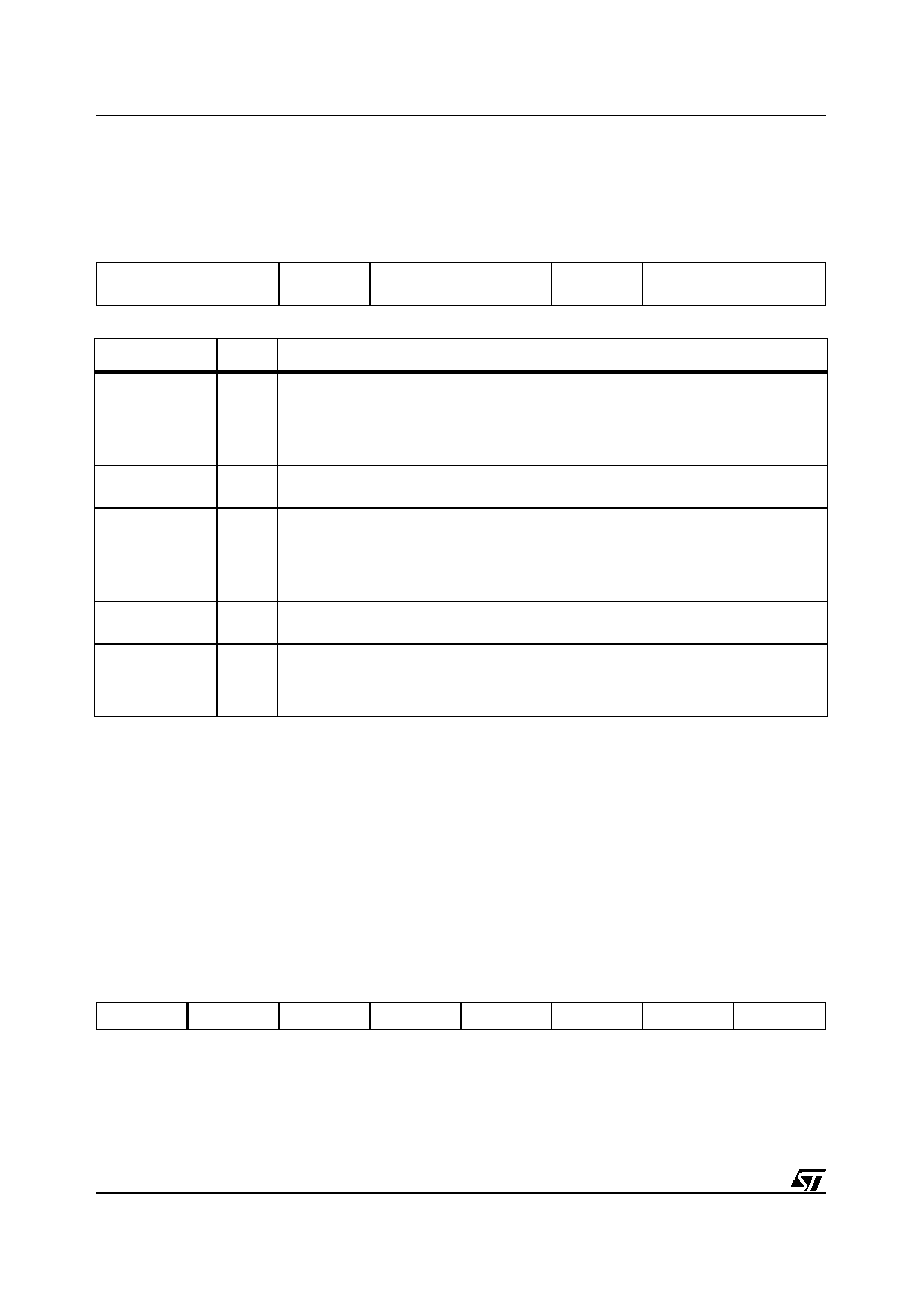
Register List
STV82x6
40/97
ANA_SCART
SCART Control Register
Note:
SCART I≤C programming (matrixing and mute control) is maintained during Standby mode
Before switching to Standby mode, the output SCART mute is recommended if the demodulated
sound source (DSP_OSCART) is selected by this output. This source might cause an audible plop
during the digital power down.
ANA_LS_HP
Loudspeaker/Subwoofer/Headphone Mute Control
Address (hex): 06h
Type: R/W
Bit 7
Bit 6
Bit 5
Bit 4
Bit 3
Bit 2
Bit 1
Bit 0
DSP_ISCART_SEL[1:0]
MUTE_OSCA
RT2
OSCART2_SEL[1:0]
MUTE_OSCA
RT1
OSCART1_SEL[1:0]
Bit Name
Reset
Function
DSP_ISCART
_SEL[1:0]
00
Analog Audio Matrixing for Mono and SCART Inputs (with Low Noise Audio Switching)
00: ISCART1 (Default)
01: ISCART2
10: ISCART3
11: Mono input
MUTE_OSCART2
1
0: No Mute
1: x Output muted
OSCART2_SEL
[1:0]
01
Analog Audio Matrixing for SCART outputs (with Low Noise Audio Switching)
00: DSP_OSCART
01: ISCART1 (Default)
10: ISCART2
11: ISCART3
MUTE_OSCART1
1
0: No Mute
1: x Output muted
OSCART1_SEL
[1:0]
00
00: DSP_OSCART (Default)
01: ISCART1
10: ISCART2
11: ISCART3
ANA_LS/HP
Address (hex): 07h
Type: R/W
Bit 7
Bit 6
Bit 5
Bit 4
Bit 3
Bit 2
Bit 1
Bit 0
HPD_IN
HPD_ON
SW_ON
0
0
MUTE_LS
MUTE_SW
MUTE_HP
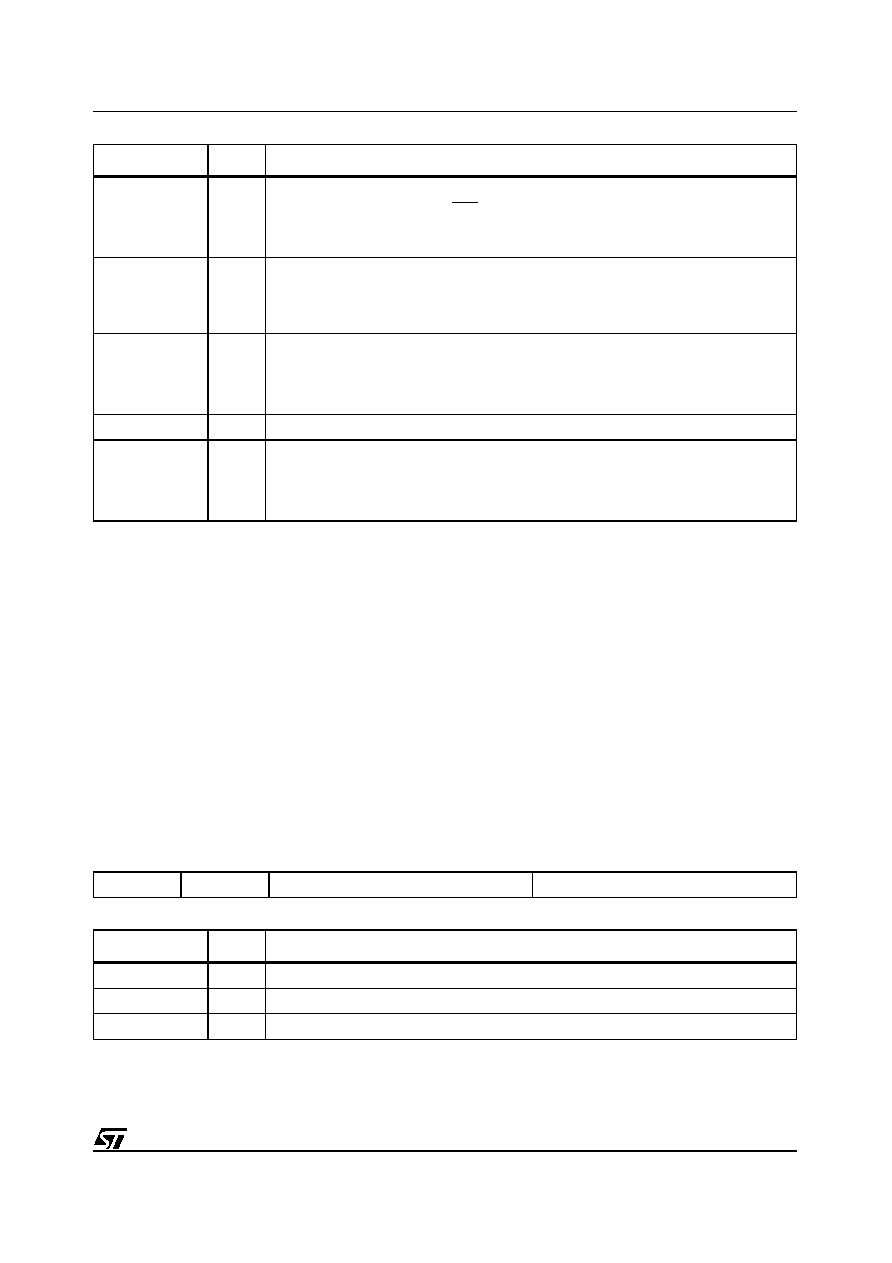
41/97
STV82x6
Register List
9.4
Clocking
A low-jitter PLL Clock is integrated and can be fully reprogrammed using the registers described
below. By default, the programming is defined for a 27-MHz quartz crystal frequency, which is the
frequency recommended for reducing potential RF interference in the application. (See
Section
2.2: System Clock
.) However, if necessary, the PLL Clock can be re-programmed for other quartz
crystal frequencies within a range from 23 to 30 MHz. Other quartz crystal frequencies can be
programmed on your demand.
Note:
A Crystal Frequency change is compatible with other default I≤C programming including the built-in
Automatic Standard Recognition System.
PLL_DIV
PLL Frequency Divider Register
Bit Name
Reset
Function
HPD_IN
0
Headphone Input Pin Status
Read only I≤C bit that displays the HPD pin Status
0: Headphone is detected
1: Headphone is not detected
HPD_ON
0
Headphone Detection Enable
0: Headphone Detection is disabled
1: Headphone Detection is enabled. If the HPD_IN bit is set, the Loudspeaker and Subwoofer
mute is activated
SW_ON
0
Subwoofer Enable
Before switching on/off the subwoofer, a mute is recommended to prevent an audible plop.
0: Subwoofer is disabled. Headphone output is selected.
1: Subwoofer is enabled. Subwoofer output is selected and Headphone output is in Mono mode
Bits[4:3]
00
Reserved.
MUTE_LS
MUTE_SW
MUTE_HP
000
000: LS + SW + HP mono
100: Not used.
001: LS + SW
101: Not used.
010: LS + HP stereo
110: HP stereo only.
011: LS only
111: All muted (Default)
Address (hex): 08h
Type: R/W
Bit 7
Bit 6
Bit 5
Bit 4
Bit 3
Bit 2
Bit 1
Bit 0
0
0
SDIV[2:0]
FDIV[2:0]
Bit Name
Reset
Function
Bits[7:6]
00
Reserved.
SDIV[2:0]
000
PLL Frequency S-Divider
FDIV[2:0
101
PLL Frequency F-Divider
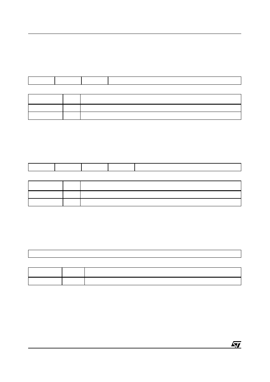
Register List
STV82x6
42/97
PLL_MD
PLL Coarse Frequency Control Register
PLL_PEH
PLL Fine Frequency Control Register (MSBs)
PLL_PEL
PLL Fine Frequency Control Register (LSBs)
Address (hex): 09h
Type: R/W
Bit 7
Bit 6
Bit 5
Bit 4
Bit 3
Bit 2
Bit 1
Bit 0
0
0
0
MD2[4:0]
Bit Name
Reset
Function
Bits[7:5]
000
Reserved.
MD2[4:0]
11110
PLL Coarse Frequency Control
Address (hex): 0Ah
Type: R/W
Bit 7
Bit 6
Bit 5
Bit 4
Bit 3
Bit 2
Bit 1
Bit 0
0
0
0
0
PE1[11:8]
Bit Name
Reset
Function
Bits[7:4]
000
Reserved.
PE1[11:8]
0001
PLL Fine Frequency Control (4 MSBs)
Address (hex): 0Bh
Type: R/W
Bit 7
Bit 6
Bit 5
Bit 4
Bit 3
Bit 2
Bit 1
Bit 0
PE1[7:0]
Bit Name
Reset
Function
PE1[7:0]
11101000
PLL Fine Frequency Control (8 LSBs)
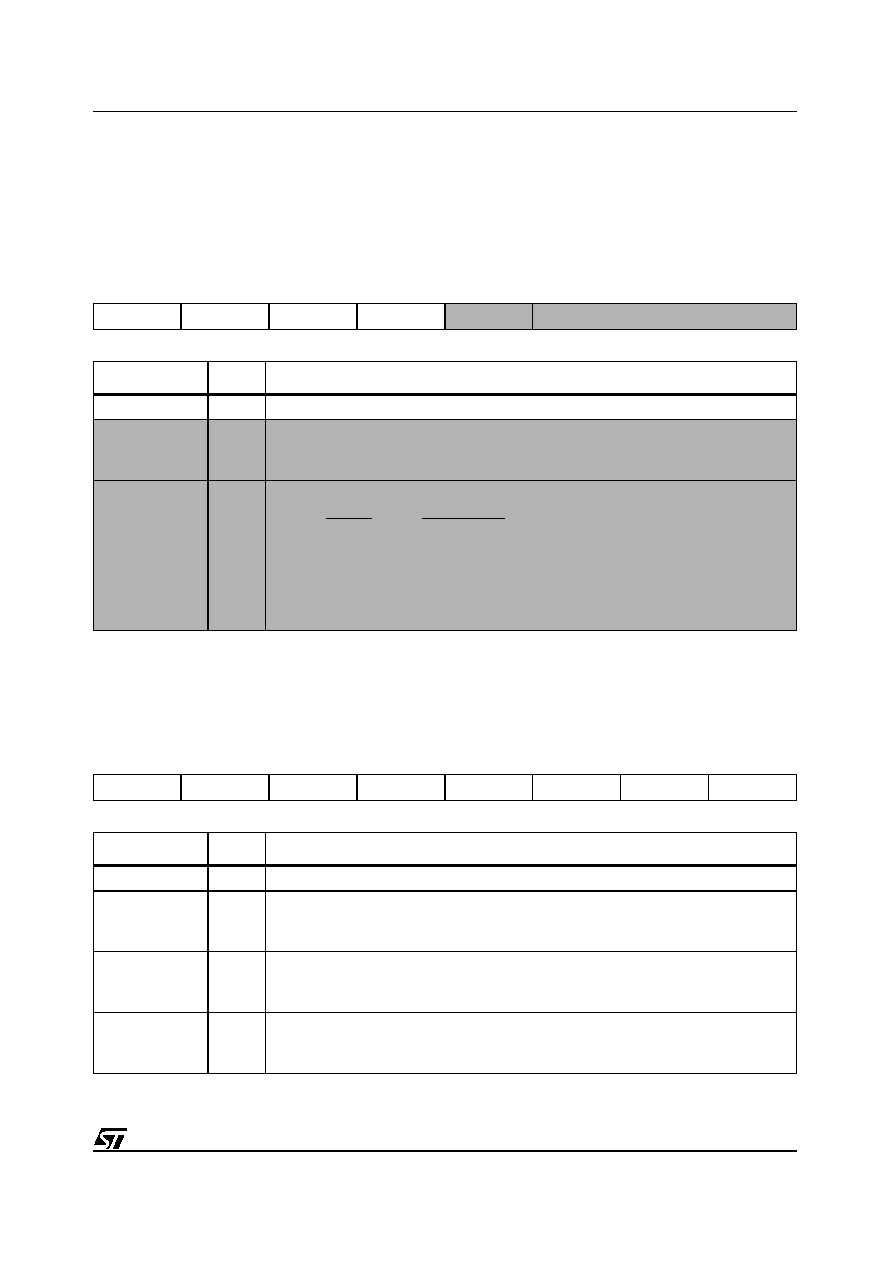
43/97
STV82x6
Register List
9.5
Demodulator
DEMOD_CTRL
Demodulator Control Register
DEMOD_STAT
Demodulator Detection Status Register
Address (hex): 0Ch
Type: R/W
Bit 7
Bit 6
Bit 5
Bit 4
Bit 3
Bit 2
Bit 1
Bit 0
0
0
0
0
AM_SEL
DEMOD_MODE[2:0]
Bit Name
Reset
Function
Bits[7:4]
0000
Reserved.
AM_SEL
0
Demodulator Configuration Select
0: FM configuration of demodulator (Default)
1: AM configuration of demodulator
DEMOD_MODE[
2:0]
110
Demodulator Mode Select
CH1 FM
CH2 FM/QPSK
X00:
Normal
FM Normal
X01:
Wide
FM Wide
010:
Normal
QPSK System B/G/L/D/K
011:
Wide
QPSK System B/G/L/D/K
110:
Normal
QPSK System I
111:
Wide
QPSK System I
Address (hex): 0Dh
Type: R
Bit 7
Bit 6
Bit 5
Bit 4
Bit 3
Bit 2
Bit 1
Bit 0
0
0
0
QPSK_LK
FM2_CAR
FM2_SQ
FM1_CAR
FM1_SQ
Bit Name
Reset
Function
Bit [7:5]
000
Reserved.
QPSK_LK
0
QPSK Lock detection flag
0: Not detected
1: Detected
FM2_CAR
0
Channel 2 FM/AM Carrier detector flag
0: Not detected
1: Detected
FM2_SQ
0
Channel 2 FM Squelch detector flag
0: Not detected
1: Detected
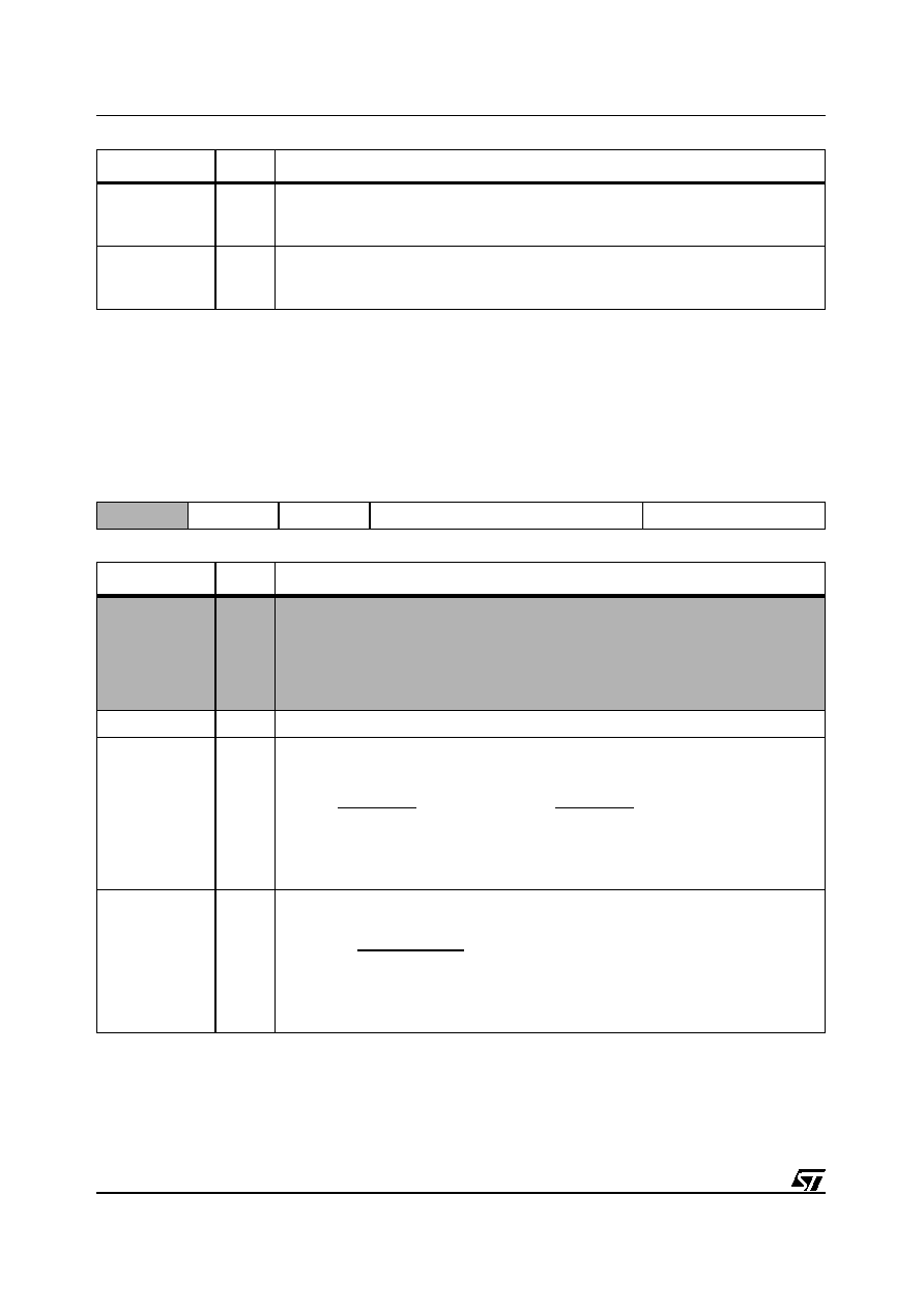
Register List
STV82x6
44/97
Note:
These registers allow direct access to the demodulator signal detectors.
AGCC
AGC Control for IF ADC
FM1_CAR
0
Channel 1 FM/AM Carrier detector flag
0: Not detected
1: Detected
FM1_SQ
0
Channel 1 FM Squelch detector flag
0: Not detected
1: Detected
Address (hex): 0Eh
Type: R/W
Bit 7
Bit 6
Bit 5
Bit 4
Bit 3
Bit 2
Bit 1
Bit 0
AGC_CMD
0
0
AGC_REF[2:0]
AGC_CST[1:0]
Bit Name
Reset
Function
AGC_CMD
0
Automatic Gain Control Command Mode
Normally set to 0 enabling automatic mode. For L/L' standards, the AGC should be switched off
due to the presence of the AM sound carrier. In this case, a fixed gain value should be set using
the AGCS register.
0: Automatic mode. AGC controlled by the AUTOSTD function. (Default)
1: Manual/Forced mode
Bits[6:5]
00
Reserved.
AGC_REF[2:0]
100
This bitfield is used to defines the clipping level which adjusts the allowable proportion of samples
at the input of the ADC which will be clipped. The AGC tries to maximize the use of the full scale
range of the ADC. The default setting gives a ratio of 1/256.
Clipping Ratio
Clipping Ratio
000:
1/16 (Single carrier)
100:
1/256 (Default
001:
1/32
101:
1/512
010:
1/64
110:
1/1024
011:
1/128
111:
1/2048 (Multiple carriers)
AGC_CST[1:0]
01
AGC Time Constant
This is the time constant between each step of 1.25 dB by the ADC.
Step Duration (ms)
00
1.33
01
2.66
10
5.33
11
10.66
Bit Name
Reset
Function
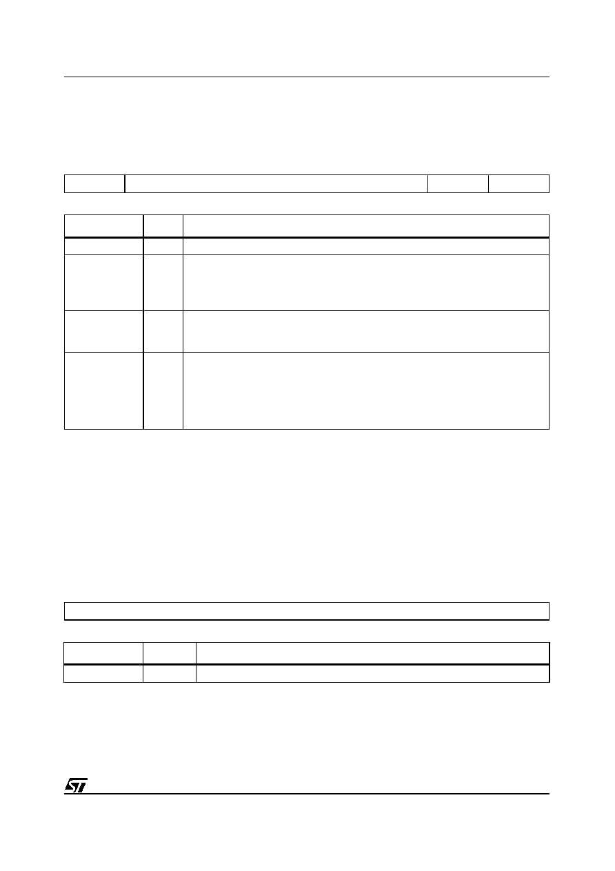
45/97
STV82x6
Register List
AGCS
AGC Control and Status for IF ADC
Note:
When AGC_CMD = 0, AGC_ERR[4:0] can be read -- indicating the input level. It can also be written
to -- presetting the AGC level which will then adjust itself to the final value.
When AGC_CMD = 1, the AGC is off and writing to AGC_ERR[4:0] directly controls the AGC
amplifier gain. Reading AGC_ERR just confirms the fixed value.
DCS
DC Offset Status for IF ADC
Address (hex): 0Fh
Type: R
Bit 7
Bit 6
Bit 5
Bit 4
Bit 3
Bit 2
Bit 1
Bit 0
0
AGC_ERR[4:0]
SIG_OVER
SIG_UNDER
Bit Name
Reset
Function
Bit 7
0
Reserved.
AGC_ERR[4:0]
00000
Amplifier Gain Control
This is the Gain Control value of ADC. There are 31 steps of +1.25 dB (see Note below).
00000: 0 dB Gain
11110: +37.5 dB Gain
SIG_OVER
0
AGC Input SIgnal Upper Threshold
0: Normal signal
1: Signal too large and AGC is overloaded
SIG_UNDER
0
AGC Input SIgnal Lower Threshold
0: Normal signal
1: Signal too small and AGC is underloaded
When the AGC is in Automatic mode (AGC_CMD = 0), bits SIG_OVER and SIG_UNDER indicate
if the input signal is too small/large and the AGC is under/overloaded. This is useful when setting
the STV82x6 SIF input level.
Address (hex): 10h
Type: R
Bit 7
Bit 6
Bit 5
Bit 4
Bit 3
Bit 2
Bit 1
Bit 0
DC_ERR[7:0]
Bit Name
Reset
Function
DC_ERR[7:0]
00000000
DC offset error of IF ADC output
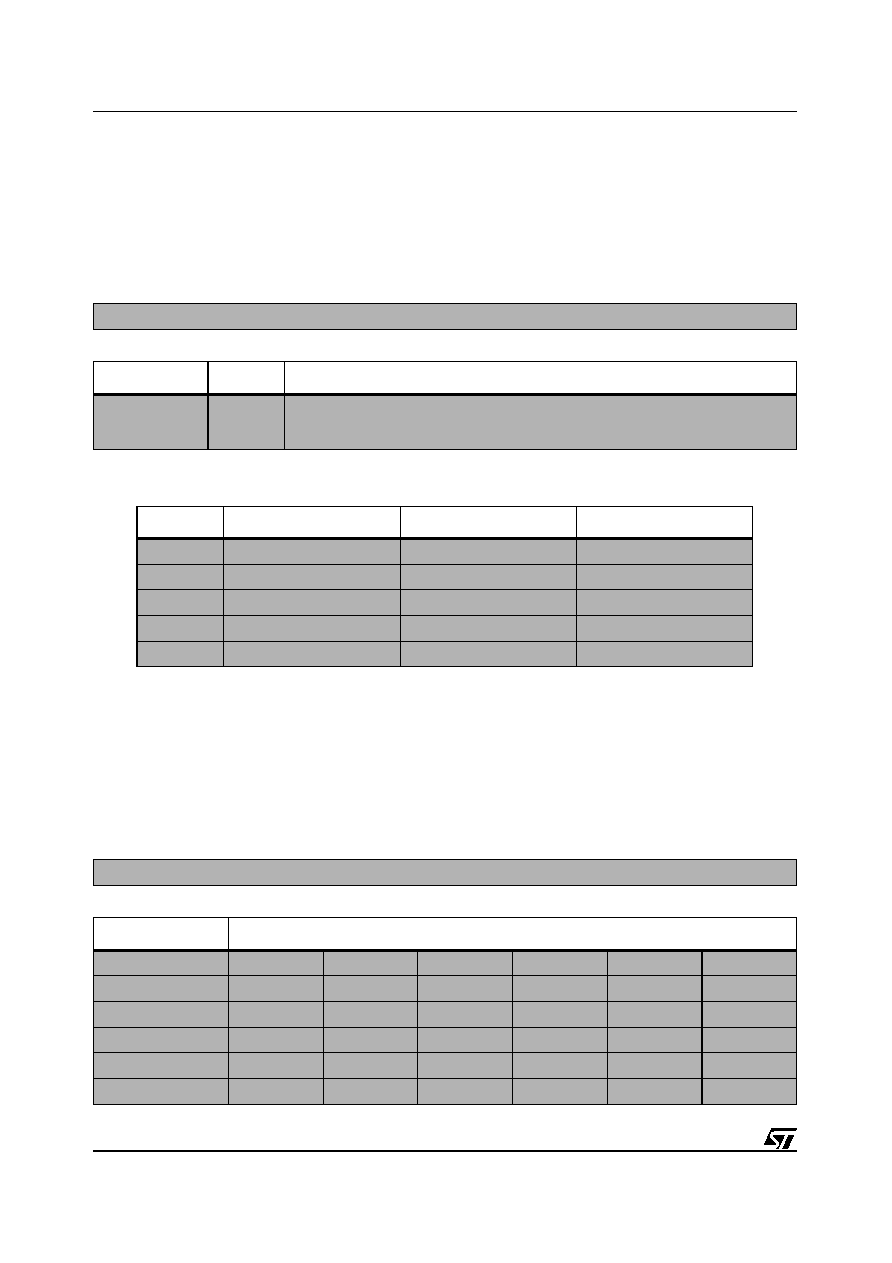
Register List
STV82x6
46/97
9.6
Demodulator Channel 1
CARFQ1H, CARFQ1M, CARFQ1LChannel 1 Carrier DCO Frequency
Note:
Carrier Freq: CARFQ1(dec).Fs/2
24
with Fs = 24.576 MHz (crystal oscillator frequency independent)
FIR1C[0:7]
Channel 1 FIR Coefficients
Address (hex): 13h to 15h
Type: R/W
Bit 7
Bit 6
Bit 5
Bit 4
Bit 3
Bit 2
Bit 1
Bit 0
CARFQ1[23:16], CARFQ1[15:8], CARFQ1[7:0]
Bit Name
Reset
Function
CARFQ1[13:8]
]CARFQ1[13:8]
CARFQ1[7:0]
00111110
10000000
00000000
Channel 1 DCO Carrier Frequency (8 MSBs)
Channel 1 DCO Carrier Frequency
Channel 1 DCO Carrier Frequency (8LSBs)
Table 11: Mono Carrier Frequencies by System
System
Mono Carrier Freq. (MHz)
CARFQ1[23:0] (dec)
CARFQ1[23:0] (hex)
M/N
4.5
3072000
2EE000h
B/G
5.5
3754667
394AABh
I
6.0
4096000
3E8000h
L
6.5
4453717
43F555h
D/K/K1/K2
6.5
4437333
43B555h
Address (hex): 15h to 1Ch
Type: R/W
Bit 7
Bit 6
Bit 5
Bit 4
Bit 3
Bit 2
Bit 1
Bit 0
FIR1C0[7:0] to FIR1C7[7:0]
Bitfield
Description
FM 27 kHz
FM 50 kHz
FM 200 kHz
FM 350 kHz
FM 500 kHz
AM
FIR1C0[7:0]
FFh
00h
00h
02h
01h
00h
FIR1C1[7:0]
FEh
FEh
01h
01h
00h
FEh
FIR1C2[7:0]
FEh
FCh
01h
FCh
04h
FDh
FIR1C3[7:0]
00h
FDh
FCh
03h
FAh
FEh
FIR1C4[7:0]
06h
02h
08h
04h
05h
04h
47/97
STV82x6
Register List
ACOEFF1
Channel 1 Baseband PLL Loop Filter Proportional Coefficient
BCOEFF1
Channel 1 Baseband PLL Loop Filter Integral Coefficient &
DCO Gain
FIR1C5[7:0]
0Eh
0Dh
F6h
F2h
00h
0Dh
FIR1C6[7:0]
16h
18h
F8h
06h
F2h
16h
FIR1C7[7:0]
1Bh
1Fh
4Ah
43h
4Dh
1Dh
Address (hex): 1Dh
Type: R/W
Bit 7
Bit 6
Bit 5
Bit 4
Bit 3
Bit 2
Bit 1
Bit 0
ACOEFF1[7:0]
Bit Name
Reset
Function
ACOEFF1[7:0]
00100011
Used to program the Proportional Coefficient of the baseband PLL loop filter (Channel 1)
Defines the damping factor of the loop. For values, refer to
Table 12
.
Address (hex): 1Eh
Type: R/W
Bit 7
Bit 6
Bit 5
Bit 4
Bit 3
Bit 2
Bit 1
Bit 0
BCOEFF1[7:0]
Bit Name
Reset
Function
BCOEFF1[7:0]
00010010
Used to program the Integral Coefficient of the baseband PLL loop filter and DCO gain
Defines the bandwidth of the loop. For values, refer to
Table 12
.
Table 12: Baseband PLL Loop Filter Adjustment (FM Mode)
FM Mode
Small
Standard
Medium
Large
A2 Standard
ACOEFF (hex)
10h
22h
2Ch
2Ch
10h
BCOEFF (hex)
1Ah
12h
0Ah
0Ah
11h
FM_DEV max (kHz)
62.5
125
250
500
125
DCO Range (kHz)
96
192
384
768
192
Bitfield
Description
Register List
STV82x6
48/97
CRF1
Channel 1 Baseband PLL Demodulator Offset
CETH1
Channel 1 FM/AM Carrier Level Threshold
SQTH1
Channel 1 FM Squelch Threshold Register
Address (hex): 1Fh
Type: R
Bit 7
Bit 6
Bit 5
Bit 4
Bit 3
Bit 2
Bit 1
Bit 0
CRF1[7:0]
Bit Name
Reset
Function
CRF1[7:0]
00000000
Channel 1 Carrier Recovery Frequency
Displays the instantaneous frequency offset of the Channel 1 Baseband PLL Demodulator.
Address (hex): 20h
Type: R/W
Bit 7
Bit 6
Bit 5
Bit 4
Bit 3
Bit 2
Bit 1
Bit 0
CETH1[7:0]
Bit Name
Reset
Function
CETH1[7:0]
00100000
This register is used to compare the carrier level in the channel and the threshold value. This
level is measured after the channel filter and is relative to the full scale reference level (0 dB).
This is used as part of the validation of an FM signal, if the carrier level is below the threshold,
the signal is considered to be non-valid.
CETH
Threshold (dB)
CETH
Threshold (dB)
FFh
-6
10h
-32 (Recommended Value)
80h
-12 08h
-38
40h
-18
00h
OFF (all carrier levels are accepted)
20h
-24 (Default)
Address (hex): 21h
Type: R/W
Bit 7
Bit 6
Bit 5
Bit 4
Bit 3
Bit 2
Bit 1
Bit 0
SQTH1[7:0]
49/97
STV82x6
Register List
CAROFFSET1
Channel 1 DCO Carrier Offset Compensation
9.7
Demodulator Channel 2
IAGCR
Channel 2 Internal AGC Reference for QPSK
Bit Name
Reset
Function
SQTH1[7:0]
00111100
The squelch detector measures the level of high frequency noise (> 40 kHz) and compares it to
the threshold level (SQTH). If the level is below this value, the S/N of the FM signal is
considered to be acceptable. Values are given for FM with standard deviation.
SQTH
S/N (dB)
FAh
0
77h
10
3Ch
15 (Default)
23h
20
19h
25
Address (hex): 22h
Type: R/W
Bit 7
Bit 6
Bit 5
Bit 4
Bit 3
Bit 2
Bit 1
Bit 0
CAROFFSET1[7:0] (S)
Bit Name
Reset
Function
CAROFFSET1[7:0]
00000000
This value is used correct the carrier frequency offset of the incoming IF signal. Automatic
frequency control in FM mode can be implemented by registers
FM_DCR
and
FM_DCL
.
A DCO frequency offset (in two's complement format) is added to the pre-programming value
by AUTOTSD in the CARFQ1 registers (corresponding to the standard IF carrier frequency).
The programmable carrier offset ranges from -192 kHz to +190.5 kHz with a resolution of
1.5 kHz.
For standard FM deviation, the value displays by FM_DCL can be directly loaded in
CAROFFSET1 to exactly compensate the carrier offset on Channel 1
Address (hex): 25h
Type: R/W
Bit 7
Bit 6
Bit 5
Bit 4
Bit 3
Bit 2
Bit 1
Bit 0
IAGC_REF[7:0]
Bit Name
Reset
Function
IAGC_REF[7:0]
10001000
Sets the mean value of the internal AGC, used for QPSK demodulation. The default setting
corresponds to half full scale amplitude at the baseband PLL input.
Register List
STV82x6
50/97
IAGCC
Channel 2 Internal AGC Time Constant for QPSK
IAGCS
Channel 2 Internal AGC Status for QPSK
CARFQ2H, CARFQ2M, CARFQ2LChannel 2 Carrier DCO Frequency
Address (hex): 26h
Type: R/W
Bit 7
Bit 6
Bit 5
Bit 4
Bit 3
Bit 2
Bit 1
Bit 0
IAGC_OFF
0
0
0
0
IAGC_CST[2:0]
Bit Name
Reset
Function
IAGC_OFF
0
AGC Disable
0: Internal AGC is active
1: Internal AGC is disabled
Bits[6:3]
0000
Reserved.
IAGC_CST[2:0]
011
Internal AGC Programmable Step Constant.
These bits control the time per step (values given for QPSK mode). The default value defines the
optimum trade-off between fast settling time (for the fastest NICAM identification) and the noise
immunity (minimum BER degradation)
Step time (us) Time Response (ms)
000
703
128
001
352
64
010
176
32
011
88
16
100
44
8
101
22
4
110
11
2
111
5.5
0.82
Address (hex): 27h
Type: R
Bit 7
Bit 6
Bit 5
Bit 4
Bit 3
Bit 2
Bit 1
Bit 0
IAGC_CTRL[7:0]
Bit Name
Reset
Function
IAGC_CTRL[7:0]
00000000
Indicates the value of the internal AGC gain control
Address (hex): 28H to 2Ah
Type: R/W
Bit 7
Bit 6
Bit 5
Bit 4
Bit 3
Bit 2
Bit 1
Bit 0
CARFQ2[23:16], CARFQ2[15.8], CARFQ2[7:0]
51/97
STV82x6
Register List
FIR2C[0:7]
Channel 2 FIR Coefficients
Bit Name
Reset
Function
CARFQ2[23:16]
CARFQ2[15.8]
CARFQ2[7:0]
01000100
01000000
00000000
Channel 2 DCO Carrier Frequency (8 MSBs)
Channel 2 DCO Carrier Frequency
Channel 2 DCO Carrier Frequency (8 LSBs) See
Table 13
.
Table 13: Stereo Carrier Frequencies by System
System
Stereo Carrier Freq. (MHz)
CARFQ2[23:0] (Dec)
CARFQ2[23:0] (Hex)
M/N A2+
4.724212
3225062
3135E6h
B/G NICAM
5.85
3993600
3CF000h
BG A2
5.7421875
3920000
3BD080h
I NICAM
6.552
4472832
444000h
L NICAM
5.85
3993600
3CF000h
DK NICAM
5.85
3993600
3CF000h
DK1 A2*
6.258125
4272000
412F80h
DK2 A2*
6.7421875
4602667
463B2Bh
DK3 A2*
5.7421875
3920000
3BD080h
Address (hex): 2Bh to 32h
Type: R/W
Bit 7
Bit 6
Bit 5
Bit 4
Bit 3
Bit 2
Bit 1
Bit 0
FIR2C0[7:0] to FIR2C7[7:0]
Table 14: Channel 2 FIR Coefficients
Bitfield
Description
FM 27 kHz
FM 50 kHz
QPSK 40%
QPSK100%
FIR2C0[7:0]
FFh
00h
00h
00h
FIR2C1[7:0]
FEh
FEh
00h
00h
FIR2C2[7:0]
FEh
FCh
FFh
00h
FIR2C3[7:0]
00h
FDh
03h
00h
FIR2C4[7:0]
06h
02h
00h
FFh
FIR2C5[7:0]
0Eh
0Dh
F4h
04h
FIR2C6[7:0]
16h
18h
0Ah
14h
FIR2C7[7:0]
1Bh
1Fh
3Dh
25h
Register List
STV82x6
52/97
ACOEFF2
Channel 2 Baseband PLL Loop Filter Proportional Coefficient
BCOEFF2
Channel 2 Baseband PLL Loop Filter Integral Coefficient &
DCO Gain
Address (hex): 33h
Type: R/W
Bit 7
Bit 6
Bit 5
Bit 4
Bit 3
Bit 2
Bit 1
Bit 0
ACOEFF2[7:0]
Bit Name
Reset
Function
ACOEFF2[7:0]
10010000
This value defines the loop clamping factor used to program the Proportional Coefficient of the
baseband PLL loop filter (Channel 2). See
Table 15
and
Table 16
.
Address (hex): 34h
Type: R/W
Bit 7
Bit 6
Bit 5
Bit 4
Bit 3
Bit 2
Bit 1
Bit 0
BCOEFF2[7:0]
Bit Name
Reset
Function
BCOEFF2[7:0]
10101100
This value defines the loop bandwidth used to program the Integral Coefficient of the Baseband
PLL loop filter and DCO gain. See
Table 15
and
Table 16
.
Table 15: Baseband PLL Loop Filter Adjustments (FM Mode)
FM mode
Small
Standard
Mid
Wide
A2 standard
ACOEFF (hex)
10h
22h
2Ch
2Ch
10h
BCOEFF (hex)
1Ah
12h
0Ah
0Ah
11h
FM_DEV max (kHz)
62.5
125
250
500
125
DCO Range (kHz)
96
192
384
768
192
Table 16: Baseband PLL Loop Filter Adjustments (QPSK Mode)
QPSK mode
Small
Medium
Large
Extra-large
ACOEFF (hex)
90h
90h
90h
90h
BCOEFF (hex)
ACh
A3h
9Ah
91h
DCO_DEV max (kHz)
2.84375
5.6875
11.375
22.75
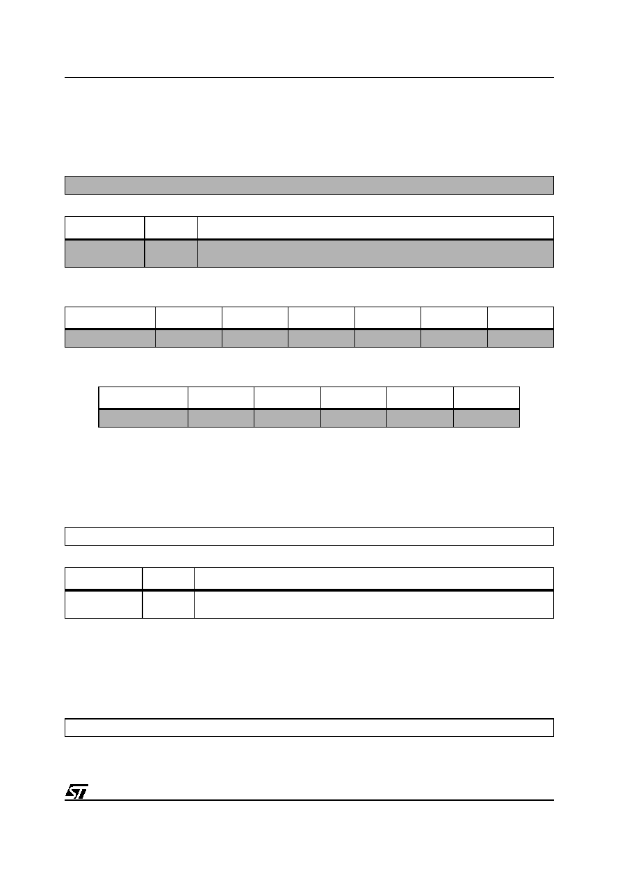
53/97
STV82x6
Register List
SCOEFF
Channel 2 Symbol Tracking Loop Coefficients
SRF
Channel 2 Symbol Tracking Loop Frequency
CRF2
Channel 2 Baseband PLL Demodulator Offset
Address (hex): 35h
Type: R/W
Bit 7
Bit 6
Bit 5
Bit 4
Bit 3
Bit 2
Bit 1
Bit 0
SCOEFF[7:0]
Bit Name
Reset
Function
SCOEFF[7:0]
00011100
This value is used to program the proportional and integral coefficients of the QPSK Symbol
tracking loop. See
Table 17
and
Table 18
.
Table 17: QPSK System - BG/L/DK Standards (40% Roll-off)
Extra-Small
Small
Medium
Large
Extra-Large
Open Loop
SCOEFF (hex)
1Eh
25h
24h
26h
2Ah
80h
Table 18: QPSK System - I Standard (100% Roll-off)
Extra-Small
Small
Medium
Large
Extra-Large
SCOEFF (hex)
16h
1Dh
1Ch
23h
22h
Address (hex): 36h
Type: R/W
Bit 7
Bit 6
Bit 5
Bit 4
Bit 3
Bit 2
Bit 1
Bit 0
SRF[7:0]
Bit Name
Reset
Function
SRF[7:0]
00000000
Displays in two's complement format the frequency deviation between the incoming NICAM
bitstream and the quartz clocks. The maximum error is ±250 ppm.
Address (hex): 37h
Type: R
Bit 7
Bit 6
Bit 5
Bit 4
Bit 3
Bit 2
Bit 1
Bit 0
CRF2[7:0]
Register List
STV82x6
54/97
CETH2
Channel 2 FM Carrier Level Threshold
SQTH2
Channel 2 FM Squelch Threshold
Bit Name
Reset
Function
CRF2[7:0]
00000000
Channel 2 Carrier Recovery Frequency.
Displays the instantaneous frequency offset of the Channel 2 Baseband PLL
Address (hex): 38h
Type: R/W
Bit 7
Bit 6
Bit 5
Bit 4
Bit 3
Bit 2
Bit 1
Bit 0
CETH2[7:0]
Bit Name
Reset
Function
CETH2[7:0]
00100000
This register is used to compare the carrier level in the channel and the threshold value. This
level is measured after the channel filter and is relative to the full scale reference level (0 dB).
This is used as part of the validation of an FM signal, if the carrier level is below the threshold,
the signal is considered to be non-valid.
CETH
Threshold (dB)
CETH
Threshold (dB)
FFh
-6
10h
-32
80h
-12 08h
-38
40h
-18
00h
OFF (All carrier levels are accepted)
20h
-24 (Default)
Address (hex): 39h
Type: R/W
Bit 7
Bit 6
Bit 5
Bit 4
Bit 3
Bit 2
Bit 1
Bit 0
SQTH2[7:0]
Bit Name
Reset
Function
SQTH2[7:0]
00111100
The squelch detector measures the level of high frequency noise (> 40 kHz) and compares it to
the threshold level (SQTH). If the level is below this value, the S/N of the FM signal is
considered to be acceptable. Values are given for FM with standard deviation.
SQTH
S/N (dB)
FAh
0
77h
10
3Ch
15 (Default)
23h
20
19h
25
55/97
STV82x6
Register List
CAROFFSET2
Channel 2 DCO Carrier Offset Compensation
9.8
NICAM Registers
NICAM_CTRL
NICAM Decoder Control Register
Address (hex): 3Ah
Type: R/W
Bit 7
Bit 6
Bit 5
Bit 4
Bit 3
Bit 2
Bit 1
Bit 0
CAROFFSET2[7:0] (S)
Bit Name
Reset
Function
CAROFFSET2
[7:0]
00000000
This value is used to correct the carrier frequency offset of the incoming IF signal. Automatic
frequency control in FM mode can be implemented by registers
FM_DCR
and
FM_DCL
.
A DCO frequency offset (in two's complement format) is added to the pre-programming value
by AUTOTSD in the CARFQ2 registers (corresponding to the standard IF carrier frequency).
The programmable carrier offset ranges from -192 kHz to +190.5 kHz with a resolution of
1.5 kHz.
For standard FM deviation, the value displayed by register
FM_DCR
can be directly loaded in in
register
CAROFFSET2
to exactly compensate the carrier offset on Channel 2.
Address (hex): 3Dh
Type: R/W
Bit 7
Bit 6
Bit 5
Bit 4
Bit 3
Bit 2
Bit 1
Bit 0
0
0
0
0
0
DIF_POL
ECT
MAE
Bit Name
Reset
Function
Bits[7:3]
00000
Reserved.
DIF_POL
0
0: No polarity inversion (Default)
1: Polarity inversion of the differential decoding
ECT
0
Error Counter Timer: Defines the NICAM error measurement period
0: 128 ms (Default)
1: 64 ms
MAE
0
Max. Allowed Errors. Defines the NICAM error decoding for mute function.
0: 511 Max (Default)
1: 255 Max
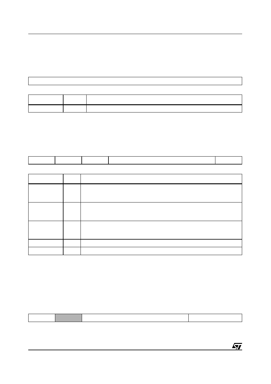
Register List
STV82x6
56/97
NICAM_BER
NICAM Bit Error Rate Register
NICAM_STAT
NICAM Detection Status Register
9.9
Zweiton
ZWT_CTRL
Zweiton Detector Control Register
Address (hex): 3Eh
Type: R
Bit 7
Bit 6
Bit 5
Bit 4
Bit 3
Bit 2
Bit 1
Bit 0
ERROR[7:0]
Bit Name
Reset
Function
ERROR[7:0]
00000000
NICAM Error Counter Value
Address (hex): 3Fh
Type: R
Bit 7
Bit 6
Bit 5
Bit 4
Bit 3
Bit 2
Bit 1
Bit 0
NIC_DET
F_MUTE
LOA
CBI[3:0]
NIC_MUTE
Bit Name
Reset
Function
NIC_DET
0
NICAM Signal Detect
0: NICAM signal no detected
1: NICAM signal detected
F_MUTE
0
Frame Mute
0: No mute
1: Mute due to Superframe Alignment Loss
LOA
0
Loss of Frame Alignment Word (FAW)
0: No Alignment Lost
1: Frame Alignment Word Lost
CBI[3:0]
0000
Indicates the received NICAM control bits
NIC_MUTE
0
Indicates the NICAM decoder mute
Address (hex): 40h
Type: R/W
Bit 7
Bit 6
Bit 5
Bit 4
Bit 3
Bit 2
Bit 1
Bit 0
0
STD_MODE
THRESH[3:0]
TSCTRL[1:0]
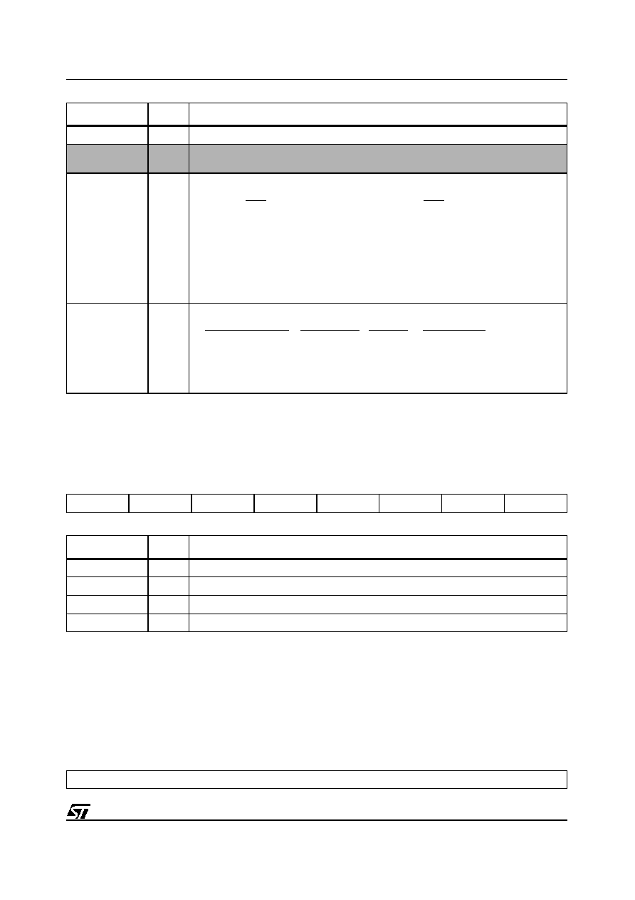
57/97
STV82x6
Register List
ZWT_STAT
Zweiton Status Register
9.10
Sound Preprocessing and Selection Registers
FM_DCL
FM DC Offset Left Register
Bit Name
Reset
Function
Bit 7
0
Reserved.
STD_MODE
0
0: German standard (Default)
1: Korean standard
THRESH[3:0]
1100
Defines the threshold of the detector for pilot and tone frequencies.
Level (% of the mid scale)
Level (% of the mid scale)
0000
0
1000
50
0001
6.25
1001
56.25
0010
12.5
1010
62.5
0011
18.75
1011
68.75
0100
25
1100 (Default)
75
0101
31.25
1101
81.25
0110
37.5
1110
87.5
0111
43.75
1111
93.75
TSCTRL[1:0]
00
Defines both the detection time and the error probability (reliability of the detection).
Sample Accumulation
Decision Count
Time (ms)
Error Probability
00
1024
2
256
10
-4
01 (Default)
1024
3
384
10
-6
10
2048
2
512
10
-7
11
2048
3
768
10
-9
Address (hex): 41h
Type: R
Bit 7
Bit 6
Bit 5
Bit 4
Bit 3
Bit 2
Bit 1
Bit 0
0
0
0
0
0
ZW_DET
ZW_ST
ZW_DM
Bit Name
Reset
Function
Bits[7:3]
00000
Reserved.
ZW_DET
0
Pilot Detection Flag
ZW_ST
0
Stereo Tone Detection Flag
ZW_DM
0
Dual Mono Tone Detection Flag
Address (hex): 42h
Type: R
Bit 7
Bit 6
Bit 5
Bit 4
Bit 3
Bit 2
Bit 1
Bit 0
FM_DCL[7:0]
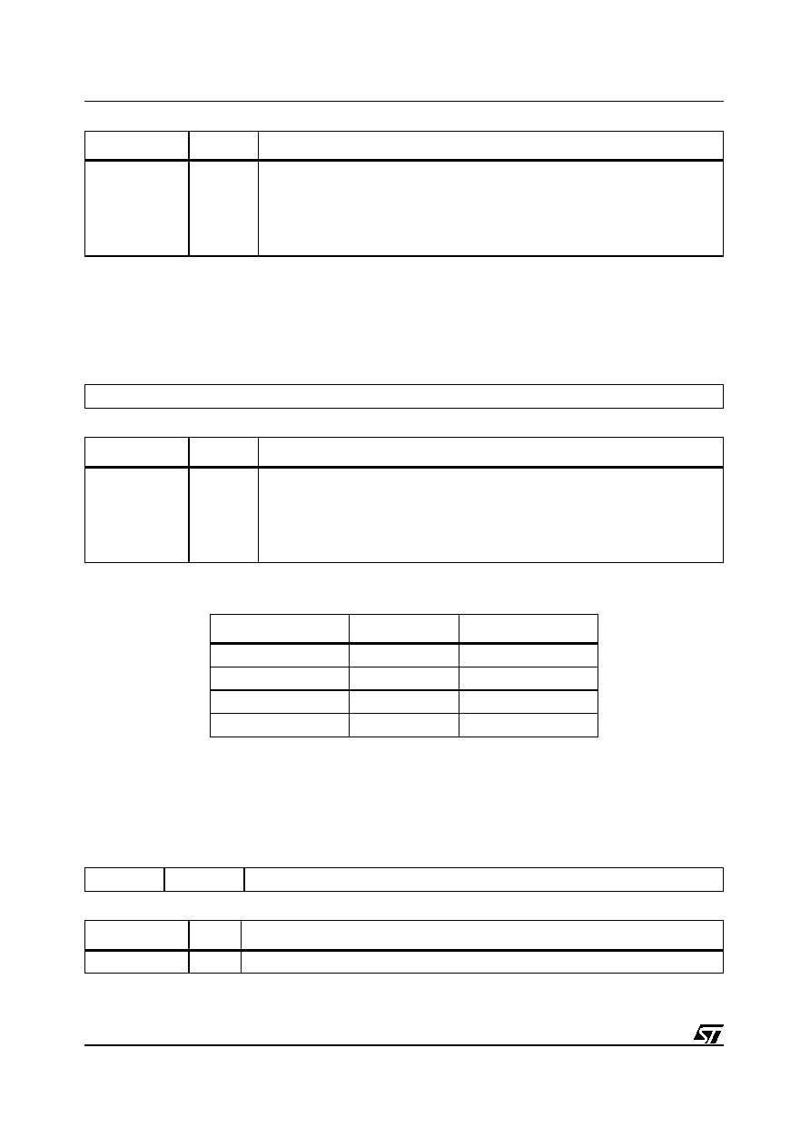
Register List
STV82x6
58/97
FM_DCR
FM DC Offset Right Register
PRE_FM
FM Prescaling Register
Bit Name
Reset
Function
FM_DCL[7:0]
00000000
Displays (in two's complement format) the FM (or AM) DC offset level after demodulation on
channel 1 (and removed automatically).
In FM mode, the DC offset value gives a direct value of the carrier frequency offset which is
used to compensate the DCO with the CAROFFSET1 value in the event of an out-of-standard
offset. The range and the resolution depend upon the FM bandwidth programmed defined in
register BCOEFF1. See
Table 19
.
Address (hex): 43h
Type: R
Bit 7
Bit 6
Bit 5
Bit 4
Bit 3
Bit 2
Bit 1
Bit 0
FM_DCR[7:0]
Bit Name
Reset
Function
FM_DCR[7:0]
00000000
Displays (in two's complement format) the FM (or AM) DC offset level after demodulation on
channel 2 (and removed automatically).
In FM mode, the DC offset value gives a direct value of the carrier frequency offset which is
used to compensate the DCO with the CAROFFSET2 value in the event of an out-of-standard
offset. The range and the resolution depend upon the FM bandwidth programmed defined in
register BCOEFF2. See
Table 19
.
Table 19: FM_DCL/R Range and Resolution
FM mode
Range (kHz)
Resolution (kHz)
Small
± 96
0.750
Standard & A2 Standard
± 192
1.5
Medium
± 384
3
Large
± 768
6
Address (hex): 44h
Type: R/W
Bit 7
Bit 6
Bit 5
Bit 4
Bit 3
Bit 2
Bit 1
Bit 0
0
0
FM_PRESCALE[5:0]
Bit Name
Reset
Function
Bits[7:6]
0
Reserved.
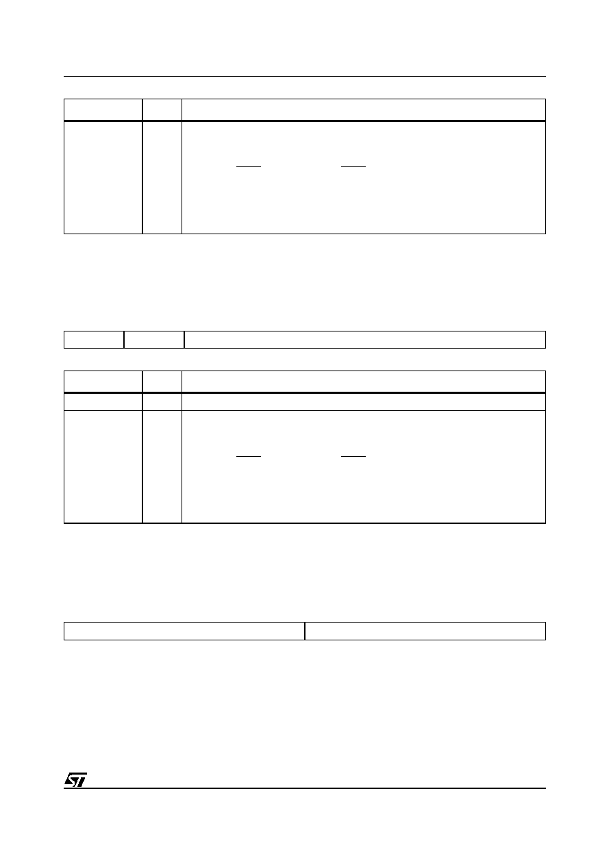
59/97
STV82x6
Register List
PRE_NICAM
NICAM Prescaling Register
PRE_AUX
SCART Prescaling Register
FM_PRESCALE
[5:0]
000110 -6 to + 24 dB FM (or AM) prescaling to normalize the FM (or AM) demodulated signal level before
audio processing. Auto level control can be implemented by I≤C software using the Peak Level
Detector. (Default value = +6 dB)
G (dB)
G (dB)
011000
+24
111110
-2
010111
+23
111101
-3
010110
+22
111100
-4
010101
+21
111011
-5
010100
+20
111010
-6
etc.
Address (hex): 45h
Type: R/W
Bit 7
Bit 6
Bit 5
Bit 4
Bit 3
Bit 2
Bit 1
Bit 0
0
0
NICAM_PRESCALE[5:0]
Bit Name
Reset
Function
Bits[7:6]
00
Reserved.
NICAM_
PRESCALE[5:0]
001101 -6 to + 24 dB NICAM prescaling to normalize the NICAM demodulated signal level before audio
processing. Auto level control can be implemented by I≤C software using the Peak Level Detector.
(Default value = +13 dB)
G (dB)
G (dB)
011000
+24
111110
-2
010111
+23
111101
-3
010110
+22
111100
-4
010101
+21
111011
-5
010100
+20
111010
-6
etc.
Address (hex): 46h
Type: R/W
Bit 7
Bit 6
Bit 5
Bit 4
Bit 3
Bit 2
Bit 1
Bit 0
I2S_PRESCALE[3:0]
SCART_PRESCALE[3:0]
Bit Name
Reset
Function
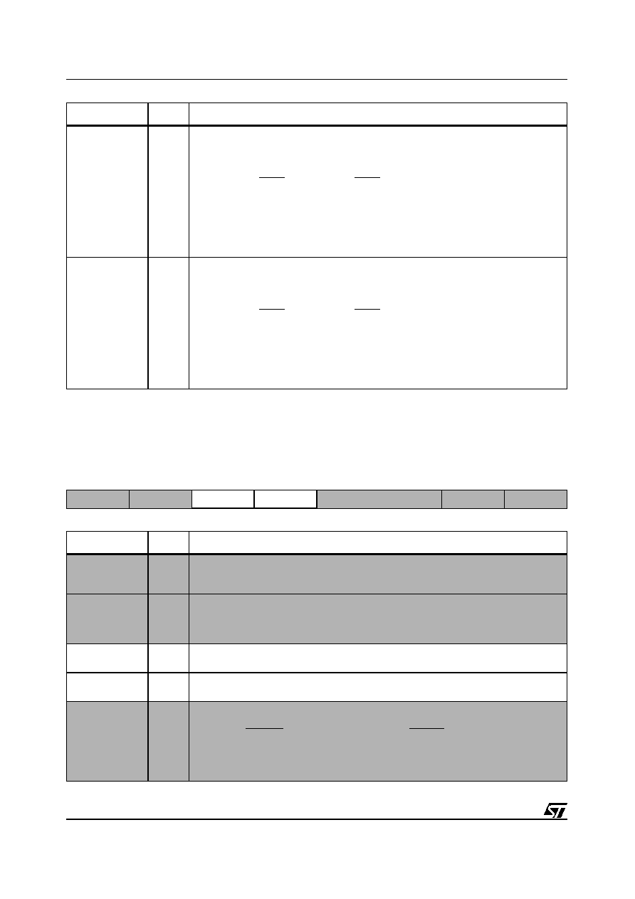
Register List
STV82x6
60/97
CH_CTRL
Channel Control Register
Bit Name
Reset
Function
I2S_PRESCALE
[3:0]
0000
-6 to + 6dB I≤S Input prescaling to normalize the incoming audio signal before audio processing.
Auto level control can be implemented by I≤C software using the Peak Level Detector.
These bits are used to adjust the corresponding incoming signal level before audio processing.
G (dB)
G (dB)
0110
+6
1111
-1
0101
+5
1110
-2
0100
+4
1101
-3
0011
+3
1100
-4
0010
+2
1011
-5
0001
+1
1010
-6
0000 (Default)
0
SCART_PRESCAL
E[3:0]
0000
-6 to + 6dB SCART Input prescaling to normalize the incoming audio signal before audio
processing. Auto level control can be implemented by I≤C software using the Peak Level Detector.
These bits are used to adjust the corresponding incoming signal level before audio processing.
G (dB)
G (dB)
0110
+6
1111
-1
0101
+5
1110
-2
0100
+4
1101
-3
0011
+3
1100
-4
0010
+2
1011
-5
0001
+1
1010
-6
0000 (Default)
0
Address (hex): 47h
Type: R/W
Bit 7
Bit 6
Bit 5
Bit 4
Bit 3
Bit 2
Bit 1
Bit 0
MUTE_D012
MUTE_D12
NIC_DMX
NICDPH_OFF
FM_DMX[1:0]
FMDPH_OFF
FMDPH_SW
Bit Name
Reset
Function
MUTE_D012
0
0: LS/HP/SC/I≤S channel unmuted
1: If DEMOD source is selected as OUTPUT channel by CH_SEL and CH_LANG,
then MUTE_LS/MUTE_HP/MUTE_SC signal are set (LS/HP/SC/I≤S channel mute)
MUTE_D12
0
0: LS/HP/SC/I≤S channel unmuted
1: If DEMOD_1 or DEMOD_2 source is selected as OUTPUT channel by CH_SEL and
CH_LANG, then MUTE_LS/MUTE_HP/MUTE_SC signal are set (LS/HP/SC/I≤S
channel mute)
NIC_DMX
0
When 1, Reverse Left/Right Channel to take into account the case where the mono signal would
be carried on the Right Channel.
NICDPH_OFF
0
0: NICAM De-emphasis (Default)
1: Bypass NICAM De-emphasis
FM_DMX[1:0]
00
FM Stereo Dematrix
DeMatrix
Standard
00 (Default)
L=CH1
,
R=CH2
No matrixing
01
L=CH1+CH2, R=CH1-CH2
Kor. Zweiton (A2+) & Radio
10
L=2CH1-CH2, R=CH2
German Zweiton (A2, A2*)
11
L=(CH1+CH2)/2, R=(CH1+CH2)/2
Stereo to Mono
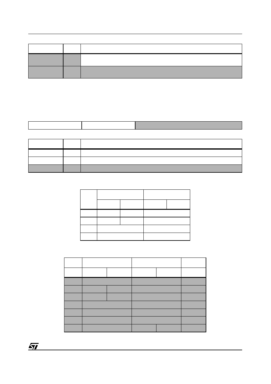
61/97
STV82x6
Register List
CH_MX
Channel Matrix Register
FMDPH_OFF
0
0: FM De-emphasis (Default)
1: Bypass FM De-emphasis
FMDPH_SW
0
0: 50 µs FM De-emphasis (Default)
1: 75 µs FM De-emphasis
Address (hex): 48h
Type: R/W
Bit 7
Bit 6
Bit 5
Bit 4
Bit 3
Bit 2
Bit 1
Bit 0
I2S_MX[1:0]
SC_MX[1:0]
DEMOD_MX[3:0]
Bit Name
Reset
Function
I2S_MX[1:0]
00
I≤S Matrixing. Programmable values are listed in
Table 20
.
SC_MX[1:0]
00
SCART Matrixing. Programmable values are listed in
Table 20
.
DEMOD_MX[3:0]
0000
Demodulator Matrixing. Programmable values are listed in
Table 21
.
Table 20: SCART and I≤S Matrixing
SC_0/I2S_0
SC_1/I2S_1
Left
Right
Left
Right
00
CH_L
CH_R
0
01
CH_R
CH_L
0
10
CH_L
CH_R
11
CH_R
CH_L
Table 21: Demodulator Matrixing
DEMOD_0
DEMOD_1
DEMOD_2
Left
Right
Left
Right
Left
0X00
FM_L
0
0
0X01
FM_L
FM_R
0
0
0X10
NIC_L
NIC_R
0
0
0X11
NIC_L
0
0
1000
FM_L
FM_R
0
1001
NIC_L
NIC_R
0
1010
FM_L
NIC_L
NIC_R
0
Bit Name
Reset
Function
Register List
STV82x6
62/97
CH_SEL
Channel Source Selection Register
Note:
A mute of the corresponding audio output is recommended before switching between Demodulated
sound and SCART source. Any audio discontinuity might create annoying audible plops.
CH_LANG
Channel Language Selection Register
Note: 1 Refer to
Table 4
and
Table 5
for selecting Channel Language, Sound and System values.
1011
FM_L
NIC_L
NIC_R
11XX
FM_L
NIC_L
0
Address (hex): 49h
Type: R/W
Bit 7
Bit 6
Bit 5
Bit 4
Bit 3
Bit 2
Bit 1
Bit 0
I2S_SEL[1:0]
SC_SEL[1:0]
HP_SEL[1:0]
LS_SEL[1:0]
Bit Name
Reset
Function
I2S_SEL[1:0]
00
Source Channel Selection.
0X: Demodulated sound (Default)
10: SCART
11: I≤S
SC_SEL[1:0]
00
HP_SEL[1:0]
00
LS_SEL[1:0]
00
Address (hex): 4Ah
Type: R/W
Bit 7
Bit 6
Bit 5
Bit 4
Bit 3
Bit 2
Bit 1
Bit 0
I2S_LANG[1:0]
SC_LANG[1:0]
HP_LANG[1:0]
LS_LANG[1:0]
Bit Name
Reset
Function
I2S_LANG[1:0]
00
Channel Language Selection. See
Table 4
and
Table 5
.
00: Not to be used.
01: Mono A
10: Mono B
11: Mono C
SC_LANG[1:0]
00
HP_LANG[1:0]
00
LS_LANG[1:0]
00
Table 21: Demodulator Matrixing (Continued)
DEMOD_0
DEMOD_1
DEMOD_2
Left
Right
Left
Right
Left
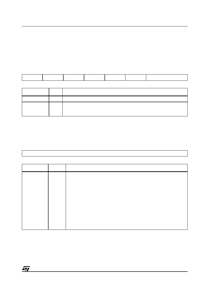
63/97
STV82x6
Register List
2 A mute of the corresponding audio output is recommended before changing the language. Any
audio discontinuity might create annoying audible plop.
PEAK_DET_CTRL
Peak Level Detector Control Register
PEAK_DET_STATL
Peak Level Detector Status Register
Address (hex): 4Bh
Type: R
Bit 7
Bit 6
Bit 5
Bit 4
Bit 3
Bit 2
Bit 1
Bit 0
0
0
0
0
0
0
PD_SEL[1:0]
Bit Name
Reset
Function
Bits[7:2]
000000 Reserved.
PD_SEL[1:0]
00
Peak Level Detector Source Selection
00: FM
10: SCART
01: NICAM
11: I≤S
Address (hex): 4Ch
Type: R
Bit 7
Bit 6
Bit 5
Bit 4
Bit 3
Bit 2
Bit 1
Bit 0
PEAK_LEVEL_LEFT[7:0]
Bit Name
Reset
Function
PEAK_LEVEL_
LEFT[7:0]
00000000
Displays the Absolute Peak Level of the audio source selected. The measured value is
updated continuously every 64 ms. The range varies linearly from the full scale (0 dB) down to 1/
256 of the full scale (-48 dB).
In AM/FM Mono mode, only the PEAK_LEVEL_LEFT[7:0] value must be taken into account.
In FM Mono mode, the audio peak level range depends upon the programmed FM bandwidth.
The unique difference is that the measurement is done after Sound pre-processing (DC offset
removal, Prescaling, De-emphasis and Dematrixing).
In FM Stereo mode, the maximum value may be used to check if the incoming signal level is
correctly adjusted by the prescaling factor or if there are no FM overmodulation problems
(clipping).
Programmable values are listed in
Table 19
.
The difference between the PEAK_LEVEL_LEFT[7:0] and PEAK_LEVEL_RIGHT[7:0] values
may be calculated by the microcontroller to identify Mono or Stereo mode from an unknown
source (SCART or I≤S).
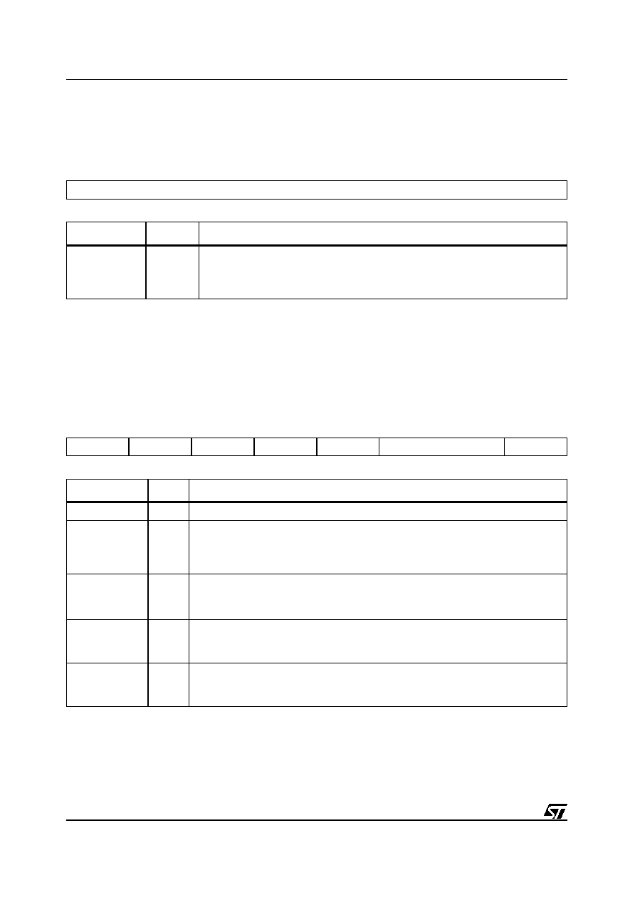
Register List
STV82x6
64/97
PEAK_DET_STATR
Peak Level Detector Status Register
9.11
Automatic Standard Recognition
AUTO_CTRL
Automatic Standard Recognition Control Register
Address (hex): 4Dh
Type: R
Bit 7
Bit 6
Bit 5
Bit 4
Bit 3
Bit 2
Bit 1
Bit 0
PEAK_LEVEL_RIGHT[7:0]
Bit Name
Reset
Function
PEAK_LEVEL_
RIGHT[7:0]
00000000
Displays the Absolute Peak Level of the audio source selected. The measured value is
updated continuously every 64 ms. The range varies linearly from the full scale (0 dB) down to
1/256 of the full scale (-48 dB).
For more information, refer to register
PEAK_DET_STATL
.
Address (hex): 50h
Type: R/W
Bit 7
Bit 6
Bit 5
Bit 4
Bit 3
Bit 2
Bit 1
Bit 0
0
0
0
IRQ
SINGLE_SHOT
DK_DEV[1:0]
LDK_SW
Bit Name
Reset
Function
Bits[7:5]
000
Reserved.
IRQ
0
This flag (output on IRQ pin) is set to ON by the AUTOSTD when the standard recognition status
has changed. The external microprocessor will detect this signal and will run the OSD procedure.
This procedure must first reset via I≤C the IRQ flag and then read the detection status in the
registers (NICAM_STAT, ZWT_STAT, AUTO_STAT and CH_MX)
SINGLE_SHOT
0
Single Shot Mode Selection
0: Single Shot mode is not selected
1: Single Shot mode is selected
1
1.
Single_Shot mode can be used before disabling the Automatic Standard Recognition (AUTOSTD)
to pre-program demodulator registers in a defined standard and reduce I≤C programming in Manual
mode
DK_DEV[1:0]
00
Selects FM deviation configuration to take into account of overmodulation in DK_NICAM standard.
00: FM 50 kHz (Default)
10: FM 350 kHz
01: FM 200 kHz
11: FM 500 kHz
LDK_SW
1
Makes exclusive the auto search of DK/K1/K2/K3 and L/L' standard
0: DK/K1/K2/K3 standard auto-search / L/L' disabled
1: L/L' standard auto-search / DK/K1/K2/K3 disabled
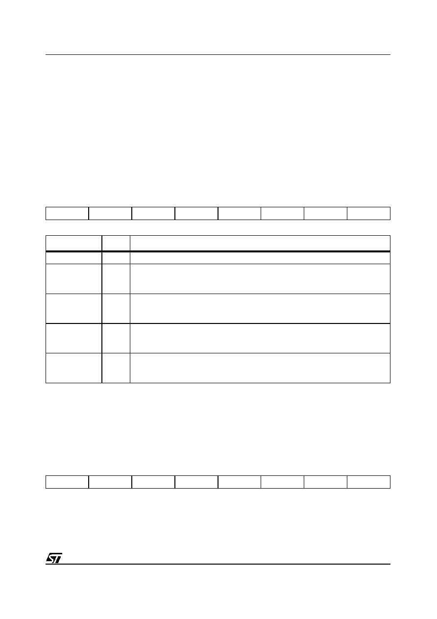
65/97
STV82x6
Register List
Note:
Only standard deviation FM 50K kHz is compatible with other D/K1/K2/K3 standards in Automatic
Standard Recognition Search mode. It has to be deselected when programs with larger FM
deviation are broadcast (reserved only for D/K-Mono or D/K NICAM standard).
FM deviation superior to 350 kHz will degrade strongly NICAM reception due to overlapping of FM
and QPSK IF spectrum in DK-NICAM standard.
L/L' and DK/K1/K2/K3 standard can be discriminated in Automatic Standard Recognition Search
mode because the same frequency is used for the mono IF carrier.
AUTO_SCKM
Auto Standard Check Mono Register
Note:
AUTOSTD is off when all mono standards are disabled.
AUTO_SCKST
Auto Standard Check Stereo Register
Address (hex): 51h
Type: R/W
Bit 7
Bit 6
Bit 5
Bit 4
Bit 3
Bit 2
Bit 1
Bit 0
0
0
0
0
LDK_SCK
I_SCK
BG_SCK
MN_SCK
Bit Name
Reset
Function
Bits[7:4]
0000
Reserved.
LDK_SCK
1
L/L' or D/K Mono Standard Enable
0: Disabled
1: Enabled
I_SCK
1
I Mono Standard Enable
0: Disabled
1: Enabled
BG_SCK
1
B/G Mono Standard Enable
0: Disabled
1: Enabled
MN_SCK
1
M/N Mono Standard Enable
0: Disabled
1: Enabled
Address (hex): 52h
Type: R/W
Bit 7
Bit 6
Bit 5
Bit 4
Bit 3
Bit 2
Bit 1
Bit 0
LDK_ZWT3
LDK_ZWT2
LDK_SWT1
LDK_NIC
I_NIC
BG_ZWT
BG_NIC
MN_ZWT
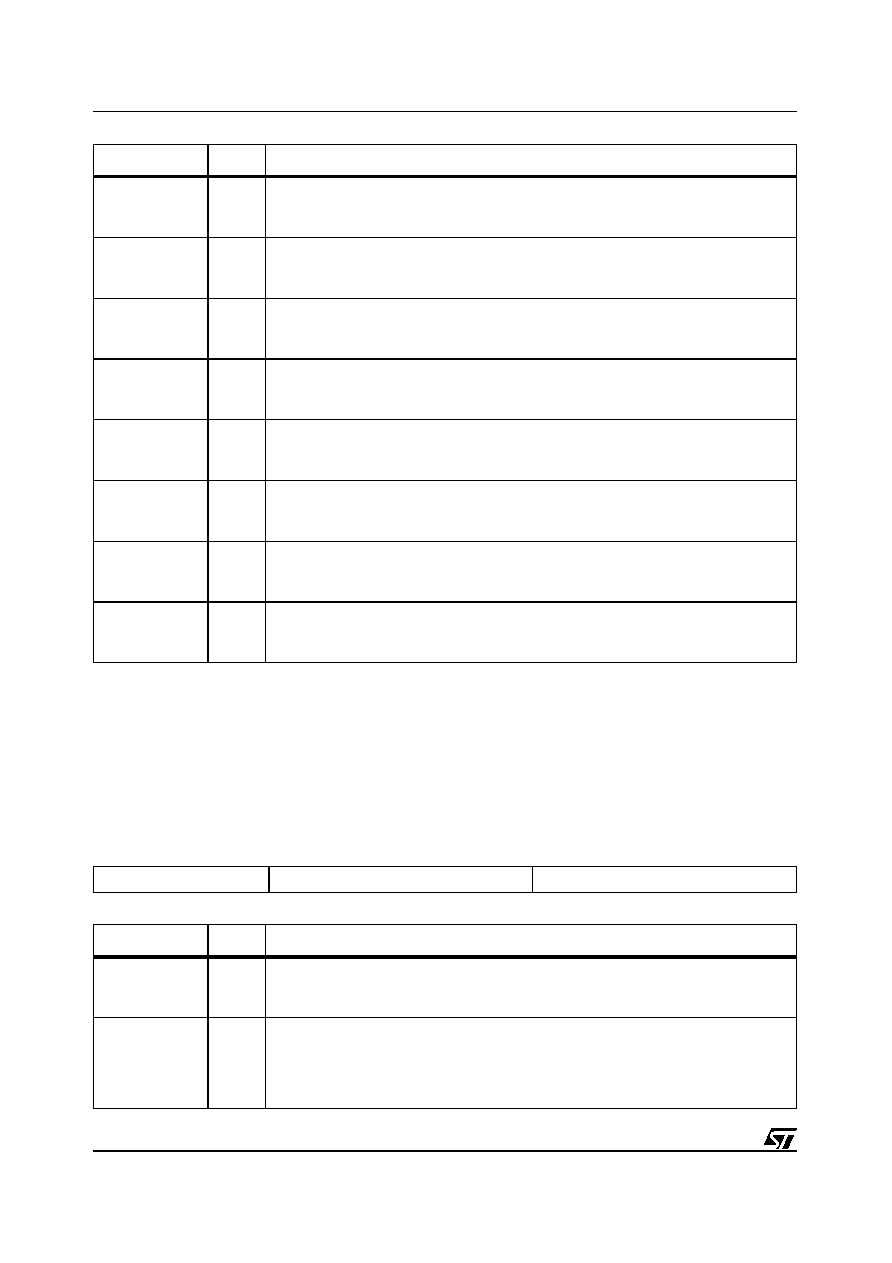
Register List
STV82x6
66/97
Note:
Stereo standard covers all transmission modes (stereo or multi-language) of the NICAM or Zweiton
(A2, A2* or A2+) system.
AUTO_TIMER
Detection Time Out Register
Bit Name
Reset
Function
LDK_ZWT3
0
D/K3 Zweiton (A2*) Stereo Standard Enable
0: Disabled
1: Enabled
LDK_ZWT2
0
D/K2 Zweiton (A2*) Stereo Standard Enable
0: Disabled
1: Enabled
LDK_ZWT1
0
D/K1 Zweiton (A2*) Stereo Standard Enable
0: Disabled
1: Enabled
LDK_NIC
1
D/K NICAM Stereo Standard Enable
0: Disabled
1: Enabled
I_NIC
1
I NICAM Stereo Standard Enable
0: Disabled
1: Enabled
BG_ZWT
1
B/G Zweiton (A2) Standard Enable
0: Disabled
1: Enabled
BG_NIC
1
B/G NICAM Standard Enable
0: Disabled
1: Enabled
MN_ZWT
1
M/N Zweiton (A2+) Standard Enable
0: Disabled
1: Enabled
Address (hex): 53h
Type: R/W
Bit 7
Bit 6
Bit 5
Bit 4
Bit 3
Bit 2
Bit 1
Bit 0
FM_TIME[1:0]
NICAM_TIME[2:0]
ZWEITON_TIME[2:0]
Bit Name
Reset
Function
FM_TIME[1:0]
10
FM Detection Time-out
00: 16 ms
10: 48 ms (Default)
01: 32 ms
11: 64 ms
NICAM_TIME[2:0]
100
NICAM Detection Time-out
000: 96 ms
100: 224 ms (Default)
001: 128 ms
101: 256 ms
010: 160 ms
110: 288 ms
011: 192 ms
111: 320 ms
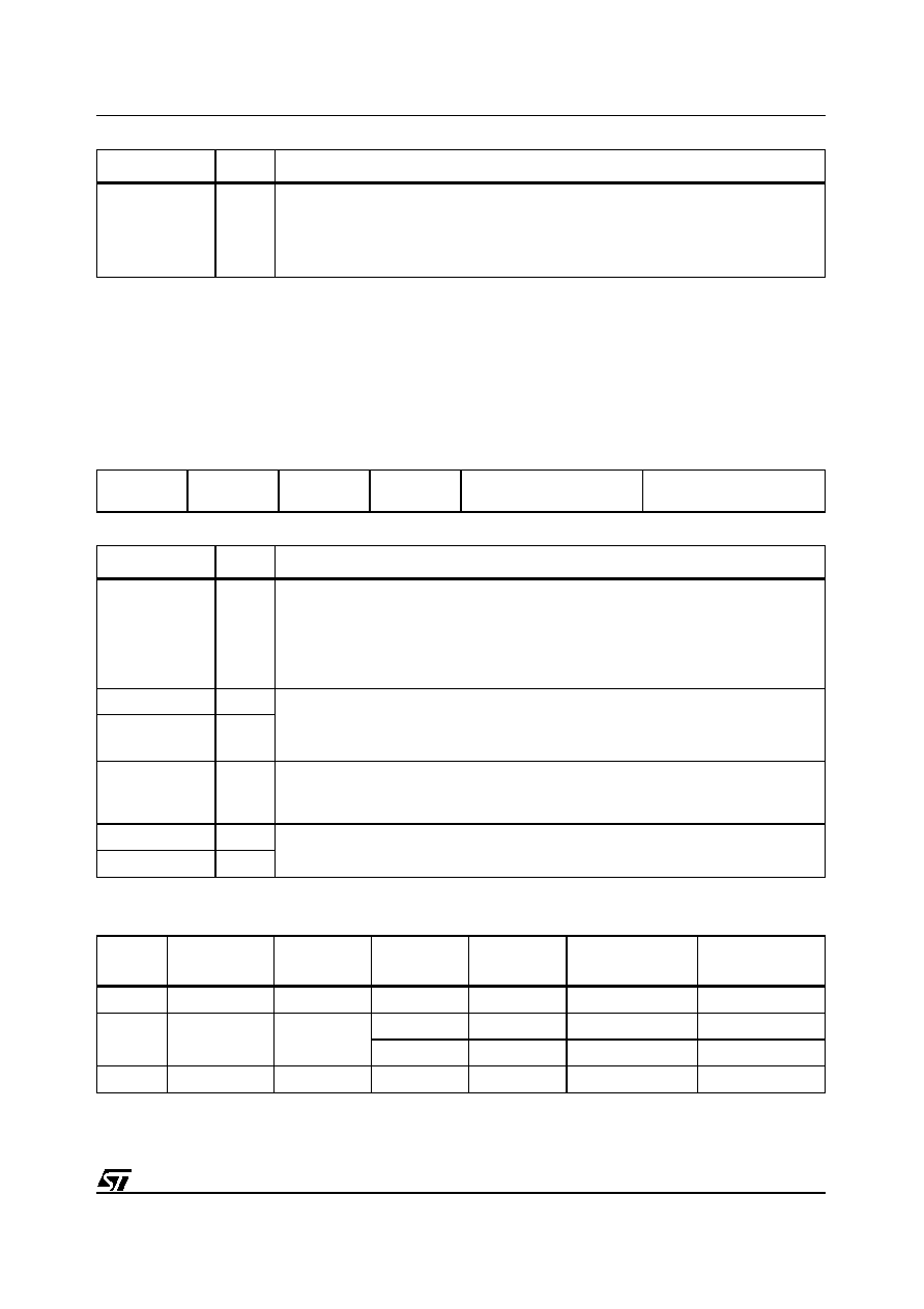
67/97
STV82x6
Register List
Note:
The time-out default value is optimum and does not normally need to be changed.
AUTO_STAT
Detection Standard Status Register
ZWEITON_TIME[
2:0]
100
Zweiton Detection Time-out
000: 256 ms
100: 1280 ms (Default)
001: 512 ms
101: 1536 ms
010: 768 ms
110: 1792 ms
011: 1024 ms
111: 2040 ms
Address (hex): 54h
Type: R
Bit 7
Bit 6
Bit 5
Bit 4
Bit 3
Bit 2
Bit 1
Bit 0
ST_ID
STEREO_STA
TE
MONO_STATE
AUTO_ON
STEREO_SID[1:0]
MONO_SID[1:0]
Bit Name
Reset
Function
ST_ID
0
Stereo Mode Detection flag activated when a stereo standard coming from the demodulator
selected on Loudspeaker output. Stereo transmission modes are:
- Zweiton stereo (ZWT_DET&ST&DM = 110, indifferently German or Korean standard)
- NICAM stereo with backup (CBI = 1000)
- NICAM stereo with no backup (CBI = 0000)
The stereo flag is also output on ST pin to control an external indicator (an LED, for instance)
STEREO_STATE
0
When AUTOSTD is ON and a standard has been detected, the FSM has two "stable states". These
flags indicate whether the FSM is in the state "mono-det" (mono standard detected) or "stereo-det"
(stereo standard detected). If at least one stereo standard is enabled, the "mono-det" state is only
transitory.
MONO_STATE
0
AUTO_ON
0
Automatic Standard Recognition System Status
0: Automatic Standard Recognition System is OFF
1: Automatic Standard Recognition System is ON
STEREO_SID[1:0]
00
Identification of the detected TV sound standard. See
Table 22
.
MONO_SID[1:0]
00
Table 22: TV Sound Standards
System
Mono Sound
(MHz)
MONO_SID
[1:0]
LDK_SW
DK_DEV
[1:0]
Stereo Sound
(MHz)
STEREO_SID
[1:0]
M/N
4.5 (FM 27k)
00
X
XX
4.724 (Zweiton A2+)
00
B/G
5.5 (FM 50k)
01
X
XX
5.85 (NICAM 40%)
00
X
XX
5.742 (Zweiton A2)
01
I
6.0 (FM 50k)
10
X
XX
6.552 (NICAM 100%)
00
Bit Name
Reset
Function
Register List
STV82x6
68/97
9.12
Smart Volume Control
SVC_SEL
SVC Selection for Loudspeaker/Headphone Register
SVC_CTRL
SVC Control Register
L
6.5 (AM)
111
1
XX
5.85 (NICAM 40%)
00
D/K
6.5 (FM 50k)
0
00
5.85 (NICAM 40%)
00
6.5 (FM 200k)
01
6.5 (FM 350k)
10
6.5 (FM 500k)
11
D/K1/K2/
K3
6.5 (FM 50k)
0
XX
5.85 (NICAM 40%)
00
0
XX
6.258 (Zweiton A2*)
01
0
XX
6.742 (Zweiton A2*)
10
0
XX
5.742 (Zweiton A2*)
11
Address (hex): 59h
Type: R/W
Bit 7
Bit 6
Bit 5
Bit 4
Bit 3
Bit 2
Bit 1
Bit 0
0
0
0
0
0
0
0
SVC_SW
Bit Name
Reset
Function
Bit[7:1]
0000000
Reserved
SVC_SW
0
Smart Volume Control Selection
0: SVC selection on Loudspeaker path
1: SVC selection on Headphone path
Address (hex): 5Ah
Type: R/W
Bit 7
Bit 6
Bit 5
Bit 4
Bit 3
Bit 2
Bit 1
Bit 0
SVC_ON
SVC_TIME[1:0]
SVC_REF[4:0]
Bit Name
Reset
Function
SVC_ON
0
Smart Volume Control Mode Select
0: Prescaling (Prevents internal clipping)
1: Automatic Level Regulation (Automatically regulates the selected sound source)
Table 22: TV Sound Standards
System
Mono Sound
(MHz)
MONO_SID
[1:0]
LDK_SW
DK_DEV
[1:0]
Stereo Sound
(MHz)
STEREO_SID
[1:0]
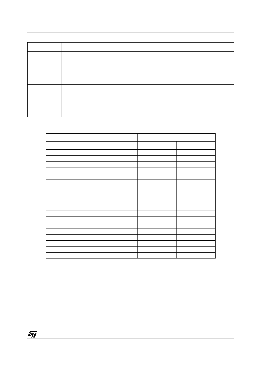
69/97
STV82x6
Register List
Note: 1 When the SVC is in Automatic mode (SVC_ON = 1), internal clipping may occur with a high
reference level (REF_LEVEL = -2.5 or -6 dB). The maximum recommended value is -8.5 dB.
2 A mute of the corresponding audio output is recommended before switching ON/OFF. A gain
discontinuity may create annoying audible plops.
SVC_TIME[1:0]
10
Defines the constant time of the gain loop.
Time Constant for 6 dB Amplification
00: 16 s
(Default)
01: 8 s
10:
4 s
11:
2 s
SVC_REF[4:0]
00000
Smart Volume Control Reference Level Select
If SVC_ON = 0, this value defines the prescaling gain ranging from -30 dB to +15.5 dB.
If SVC_ON = 1, this value defines the output reference level of the regulation ranging from -2.5 dB
down to -30 dB. The SVC output level must be adjusted to avoid internal clipping due to post-
processing with amplification, i.e. ST/SRSTM Surround Sound (+9 dB max), Equalizer or Bass/
Treble (+12 dB max) and Loudness (+6 dB max). Programmable values are listed in
Table 23
.
Table 23: SVC Bit Values
SVC_ON = 0
SVC_ON = 1
SVC_REF[4:0]
REF_LEVEL (dB)
SVC_REF[4:0]
REF_LEVEL (dB)
> 00101
Reserved
> 00101
Reserved
00101
+15.5
00101
-12
00100
+12
00100
-12
00011
+9.5
00011
-12
00010
6
00010
-12
00001
3.5
00001
-12
00000 (Default)
0
00000
-12
11111
-2.5
11111
1
-2.5
11110
-6
11110
1
-6
11101
-8.5
11101
-8.5
11100
-12
11100
-12
11011
-14.5
11011
-14.5
11010
-18
11010
-18
11001
-20.5
11001
-20.5
11000
-24
11000
-24
10111
-26.5
10111
-26.5
10110
-30
10110
-30
<10110
Reserved
< 10110
Reserved
Bit Name
Reset
Function

Register List
STV82x6
70/97
9.13
Surround
LS_SRD_CTRL
Loudspeaker Surround Control Register
LS_STS_GAIN
Loudspeaker ST WideSurround Gain Register
Address (hex): 5Bh
Type: R/W
Bit 7
Bit 6
Bit 5
Bit 4
Bit 3
Bit 2
Bit 1
Bit 0
SRD_ON
0
0
0
0
SRD_SEL
SRD_STEREO
STS_MODE
Bit Name
Reset
Function
SRD_ON
0
Surround Sound Enable
0: Surround Sound is disabled
1: Surround Sound is enabled
Bits[6:3]
0000
Reserved
SRD_SEL
0
Surround Sound Select
0: ST WideSurround Sound (Default)
1: SRSTM Surround Sound. This option is only available if the SRS_ON bit in register
CUT_ID
is
set. (STV8226/36 only)
SRD_STEREO
0
Surround Sound Stereo Mode
0: Surround Sound in Mono mode (Default)
1: Surround Sound in Stereo mode
STS_MODE
0
ST WideSurround Sound Mode Selection for Stereo Source Only
The ST_ID bit in register
AUTO_STAT
must be set.
0: ST WideSurround Sound Movie mode (Default)
1: ST WideSurround Sound Music mode
Address (hex): 5Ch
Type: R/W
Bit 7
Bit 6
Bit 5
Bit 4
Bit 3
Bit 2
Bit 1
Bit 0
STS_GAIN[7:0]
Bit Name
Reset
Function
STS_GAIN[7:0]
10000000
Defines the ST WideSurround Sound component gain in linear scale.
Level (%)
Level (%)
1000 0000 (Default)
100%
0000 0100
3.1%
0111 1111
99.2%
0000 0011
2.3%
0111 1110
98.4%
0000 0010
1.6%
0111 1101
97.6%
0000 0001
0.8%
........
0000 0000
0%
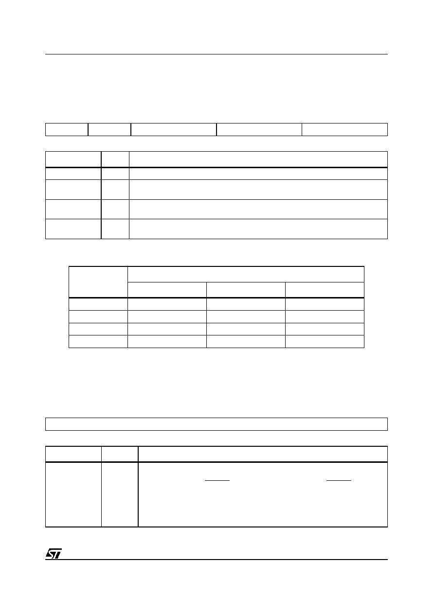
71/97
STV82x6
Register List
LS_STS_FREQ
Loudspeaker ST WideSurround Sound Frequency
LS_SRS_SPACE
Loudspeaker SRSTM Surround Sound Space Effect
Address (hex): 5Dh
Type: R
Bit 7
Bit 6
Bit 5
Bit 4
Bit 3
Bit 2
Bit 1
Bit 0
0
0
BASS_FREQ[1:0]
MEDIUM_FREQ[1:0]
TREBLE_FREQ[1:0]
Bit Name
Reset
Function
Bits[7:6]
00
Reserved.
BASS_FREQ[1:0]
01
Defines the bass frequency effect for ST WideSurround Sound. Programmable values are listed in
Table 24
.
MEDIUM_FREQ[
1:0]
01
Defines the medium frequency effect for ST WideSurround Sound in Movie or Mono mode (no
effect in Music mode). Programmable values are listed in
Table 24
.
TREBLE_FREQ[
1:0]
01
Defines the treble frequency effect for ST WideSurround Sound in Movie or Mono mode (no effect
in Music mode). Programmable values are listed in
Table 24
.
Table 24: Phase Shifter Center Frequencies
Phase Shifter Center Frequency
BASS_FREQ[1:0]
MEDIUM_FREQ[1:0]
TREBLE_FREQ[1:0]
00
40 Hz
202 Hz
2 kHz
01 (Default)
90 Hz
416 Hz
4 kHz
10
120 Hz
500 Hz
5 kHz
11
160 Hz
588 Hz
6 kHz
Address (hex): 5Eh
Type: R/W
Bit 7
Bit 6
Bit 5
Bit 4
Bit 3
Bit 2
Bit 1
Bit 0
SRS_SPACE[7:0]
Bit Name
Reset
Function
SRS_SPACE[7:0]
10000000
Defines the gain of the SRSTM Surround component (in linear scale).
Level (%)
Level (%)
1000 0000 (Default)
100%
0000 0100
3.1%
0111 1111
99.2%
0000 0011
2.3%
0111 1110
98.4%
0000 0010
1.6%
0111 1101
97.6%
0000 0001
0.8%
........
0000 0000
0%
Register List
STV82x6
72/97
LS_SRS_CENTER
Loudspeaker SRSTM Surround Sound Center Effect
9.14
5- Band Equalizer
LS_EQ_CTRL
Loudspeaker Equalizer Control Register
Address (hex): 5Fh
Type: R/W
Bit 7
Bit 6
Bit 5
Bit 4
Bit 3
Bit 2
Bit 1
Bit 0
SRS_CENTER[7:0]
Bit Name
Reset
Function
SRS_CENTER
[7:0]
10000000
Defines the gain of the SRSTM Center component (in linear scale).
Level (%)
Level (%)
1000 0000 (Default)
100%
0000 0100
3.1%
0111 1111
99.2%
0000 0011
2.3%
0111 1110
98.4%
0000 0010
1.6%
0111 1101
97.6%
0000 0001
0.8%
........
0000 0000
0%
Address (hex): 60h
Type: R/W
Bit 7
Bit 6
Bit 5
Bit 4
Bit 3
Bit 2
Bit 1
Bit 0
EQ_ON
0
0
0
0
0
0
0
Bit Name
Reset
Function
EQ_ON
0
5-Band Equalizer Enable
0: 5-Band Equalizer is disabled
1: 5-Band Equalizer is enabled (Default)
Bits[6:0]
000000 Reserved.

73/97
STV82x6
Register List
LS_EQ_BAND[1:5]
Loudspeaker Equalizer Gain
Address (hex): 61h to 65h
Type: R/W
Bit 7
Bit 6
Bit 5
Bit 4
Bit 3
Bit 2
Bit 1
Bit 0
0
0
0
EQ_BAND1_GAIN[4:0] (S)
0
0
0
EQ_BAND2_GAIN[4:0] (S)
0
0
0
EQ_BAND3_GAIN[4:0] (S)
0
0
0
EQ_BAND4_GAIN[4:0] (S)
0
0
0
EQ_BAND5_GAIN[4:0] (S)
Bit Name
Reset
Function
Bits[7:5]
000
Reserved.
EQ_BAND1_GAIN[4:0]
EQ_BAND2_GAIN[4:0]
EQ_BAND3_GAIN[4:0]
EQ_BAND4_GAIN[4:0]
EQ_BAND5_GAIN[4:0]
00000
00000
00000
00000
00000
Band Gain Adjustment within a range from -12 dB to +12 dB in steps of 1 dB.
BAND1 = Bass (Centered 100 Hz)
BAND2 = Bass-Medium (Centered 330 Hz)
BAND3 = Medium (Centered 1 kHz)
BAND4 = Treble-Medium (Centered 3.3 kHz
BAND5 = Treble (Centered 6.6 kHz)
Table 25: Loudspeaker/Headphone Equalizer Gain Values
Value
Gain G (dB)
01100
+12
01011
+11
01010
+10
................
.....
00000 (Default)
0
................
.....
10110
-10
10101
-11
10100
-12
Register List
STV82x6
74/97
9.15
Loudness/Bass & Treble
LS_LOUD
Loudspeaker Loudness Control Register
HP_BT_CTRL
Headphone Bass/Treble Control
Address (hex): 66h
Type: R/W
Bit 7
Bit 6
Bit 5
Bit 4
Bit 3
Bit 2
Bit 1
Bit 0
LOUD_ON
LOUD_TH[2:0]
LOUD_FREQ
LOUD_GHR[2:0]
Bit Name
Reset
Function
LOUD_ON
0
Loudness Enable
0: Loudness disabled
1: Loudness enabled
LOUD_TH[2:0]
000
Loudness Threshold
Programmable values are listed in
Table 26
.
LOUD_FREQ
0
Bass Cut-off Frequency Select
0: 40 Hz bass cut-off frequency (Normal mode)
1: 120 Hz bass cut-off frequency (Bass Amplified mode)
LOUD_GHR[2:0]
010
Loudness Maximum Treble Gain
Programmable values are listed in
Table 26
.
Table 26: Loudness Control Values
Bitfield Value
Threshold (dB)
LOUD_TH[2:0]
Max. Treble Gain (dB)
LOUD_GHR[2:0]
000
0 (Default)
0
001
-6
3
010
-12
6 (Default)
011
-18
9
100
-24
12
101
-30
15
110
-36
18
111
-42
Reserved
Address (hex): 71h
Type: R/W
Bit 7
Bit 6
Bit 5
Bit 4
Bit 3
Bit 2
Bit 1
Bit 0
BT_ON
0
0
0
0
0
0
0
75/97
STV82x6
Register List
HP_BASS_GAIN
Headphone Bass Gain
HP_TREBLE_GAIN
Headphone Treble Gain
Bit Name
Reset
Function
BT_ON
0
Headphone Bass/Treble Enable
0: Headphone Bass/Treble disabled
1: Headphone Bass/Treble enabled
Bit [6:0]
0
Reserved.
Address (hex): 72h
Type: R/W
Bit 7
Bit 6
Bit 5
Bit 4
Bit 3
Bit 2
Bit 1
Bit 0
0
0
0
BASS_GAIN[4:0]
Bit Name
Reset
Function
Bits[7:5]
000
Reserved
BASS_GAIN[4:0]
00000
Gain Tuning of Headphone Bass Frequency
Gain may be programmed within a range between +12 dB and -12 dB in steps of 1 dB.
Programmable values are listed in
Table 25
.
Address (hex): 73h
Type: R/W
Bit 7
Bit 6
Bit 5
Bit 4
Bit 3
Bit 2
Bit 1
Bit 0
0
0
0
TREBLE_GAIN[4:0]
Bit Name
Reset
Function
Bits[7:5]
000
Reserved
TREBLE_GAIN
[4:0]
00000
Gain Tuning of Headphone Treble Frequency
Gain may be programmed within a range between +12 dB and -12 dB in steps of 1 dB.
Programmable values are listed in
Table 25
.
Register List
STV82x6
76/97
9.16
Volume/Balance Control Registers
LS_VOL_CTRL
Loudspeaker Volume Control Register
HP_VOL_CTRL
Headphone Volume Control Register
LS_CVOL
Loudspeaker Common Volume Control Register
LS_VOL_L
Loudspeaker Left Volume Control Register
Address (hex): 67h
Type: R/W
Bit 7
Bit 6
Bit 5
Bit 4
Bit 3
Bit 2
Bit 1
Bit 0
0
0
0
0
0
0
0
BAL_MODE
Bit Name
Reset
Function
Bits[7:1]
000000 Reserved.
BAL_MODE
1
0: Independent mode.
1: Differential mode (Default)
Address (hex): 75h
Type: R/W
Bit 7
Bit 6
Bit 5
Bit 4
Bit 3
Bit 2
Bit 1
Bit 0
0
0
0
0
0
0
0
BAL_MODE
Bit Name
Reset
Function
Bits[7:1]
000000 Reserved.
BAL_MODE
1
0: Independent mode.
1: Differential mode (Default)
Address (hex): 68h
Type: R/W
Bit 7
Bit 6
Bit 5
Bit 4
Bit 3
Bit 2
Bit 1
Bit 0
CVOL[7:0] / VOL_L[7:0]
Bit Name
Reset
Function
CVOL[7:0]
00000000
Loudspeaker Common Volume
Volume may be programmed within a range between 0 dB and -96 dB in steps of 0.375 dB.
Programmable values are listed in
Table 27
.
77/97
STV82x6
Register List
HP_CVOL
Headphone Common Volume Control Register
HP_VOL_L
Headphone Left Volume Control Register
VOL_L[7:0]
00000000
Loudspeaker Left Volume
Volume may be programmed within a range between 0 dB and -96 dB in steps of 0.375 dB.
Programmable values are listed in
Table 27
.
Address (hex): 76h
Type: R/W
Bit 7
Bit 6
Bit 5
Bit 4
Bit 3
Bit 2
Bit 1
Bit 0
CVOL[7:0] / VOL_L[7:0]
Bit Name
Reset
Function
CVOL[7:0]
00000000
Headphone Common Volume
Volume may be programmed within a range between 0 dB and -96 dB in steps of 0.375 dB.
Programmable values are listed in
Table 27
.
VOL_L[7:0]
00000000
Headphone Left Volume
Volume may be programmed within a range between 0 dB and -96 dB in steps of 0.375 dB.
Programmable values are listed in
Table 27
.
Table 27: Common or Left Volume Control Values
Register Value
Volume Level (dB)
1111 1111
0 (1 V
RMS
)
1111 1110
-0.375
1111 1101
-0.75
................
.....
1000 0000 (Default)
-48
................
.....
0000 0010
-94.50
0000 0001
-95.25
0000 0000
-95.625
Bit Name
Reset
Function
Register List
STV82x6
78/97
LS_BAL
Loudspeaker Balance Control Register
LS_VOL_R
Loudspeaker Right Volume Control Register
HP_BAL
Headphone Balance Control Register
HP_VOL_R
Headphone Right Volume Control Register
Address (hex): 69h
Type: R/W
Bit 7
Bit 6
Bit 5
Bit 4
Bit 3
Bit 2
Bit 1
Bit 0
BAL[7:0] / VOL_R[7:0]
Bit Name
Reset
Function
BAL[7:0]
00000000
Loudspeaker Differential Balance
In Differential mode, the balance may be programmed in steps of 0.75 dB. Programmable
values are listed in
Table 28
.
VOL_R[7:0]
00000000
Loudspeaker Right Volume Control
In Independent mode, the volume may be programmed within a range between 0 dB and
-96 dB in steps of 0.375 dB. Programmable values are listed in
Table 29
.
Address (hex): 77h
Type: R/W
Bit 7
Bit 6
Bit 5
Bit 4
Bit 3
Bit 2
Bit 1
Bit 0
BAL[7:0] / VOL_R[7:0]
Bit Name
Reset
Function
BAL[7:0]
00000000
Headphone Differential Balance
In Differential mode, the balance may be programmed in steps of 0.75 dB. Programmable
values are listed in
Table 28
.
VOL_R[7:0]
00000000
Headphone Right Volume Control
In Independent mode, the volume may be programmed within a range between 0 dB and
-96 dB in steps of 0.375 dB. Programmable values are listed in
Table 29
.
Table 28: Differential Balance Control Values
Register Value
Left/Common Level
Right/Common Level
0111 1111 (7Fh)
-95.25 dB
0.78%
0 dB
100%
0111 1110
-94.50 dB
0.56%
0 dB
100%
0111 1101
-93.75 dB
2.34%
0 dB
100%
................
.....
.....
0000 0000 (Default)
0 dB
100%
0 dB
100%
................
.....
.....
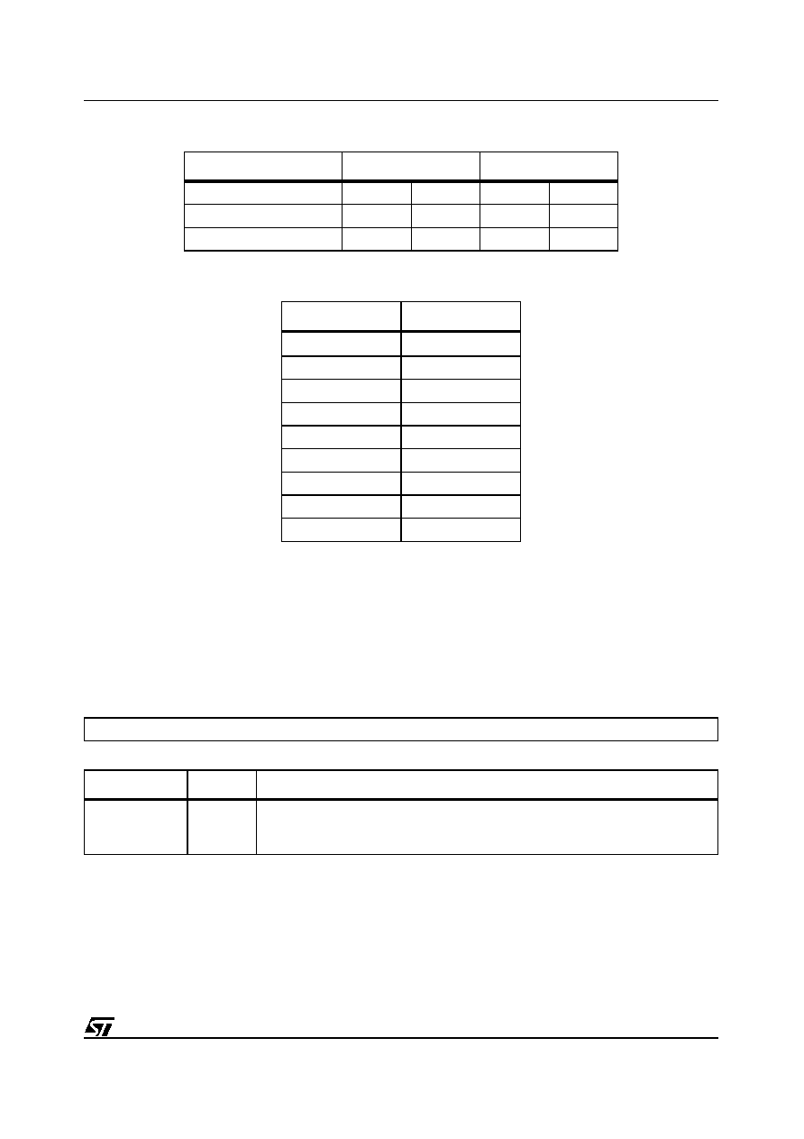
79/97
STV82x6
Register List
9.17
Subwoofer
SW_GAIN
Subwoofer Gain
1000 0010
0 dB
100%
-94.50 dB
1.56%
1000 0001
0 dB
100%
-95.25 dB
0.78%
1000 0000 (80h)
0 dB
100%
-96.00 dB
0.00%
Table 29: Right/Left Volume Control Values
Register Value
Volume Level (dB)
1111 1111
0 (1 V
RMS
)
1111 1110
-0.375
1111 1101
-0.75
................
.....
1000 0000 (Default)
-48
................
.....
0000 0010
-94.50
0000 0001
-95.25
0000 0000
-95.625
Table 28: Differential Balance Control Values
Register Value
Left/Common Level
Right/Common Level
Address (hex): 6Ah
Type: R/W
Bit 7
Bit 6
Bit 5
Bit 4
Bit 3
Bit 2
Bit 1
Bit 0
SW_GAIN[7:0]
Bit Name
Reset
Function
SW_GAIN[7:0]
10000000
Subwoofer Gain
Gain may be programmed within a range between 0 dB and -96 dB in steps of 0.375 dB.
Programmable values are listed in
Table 27
.
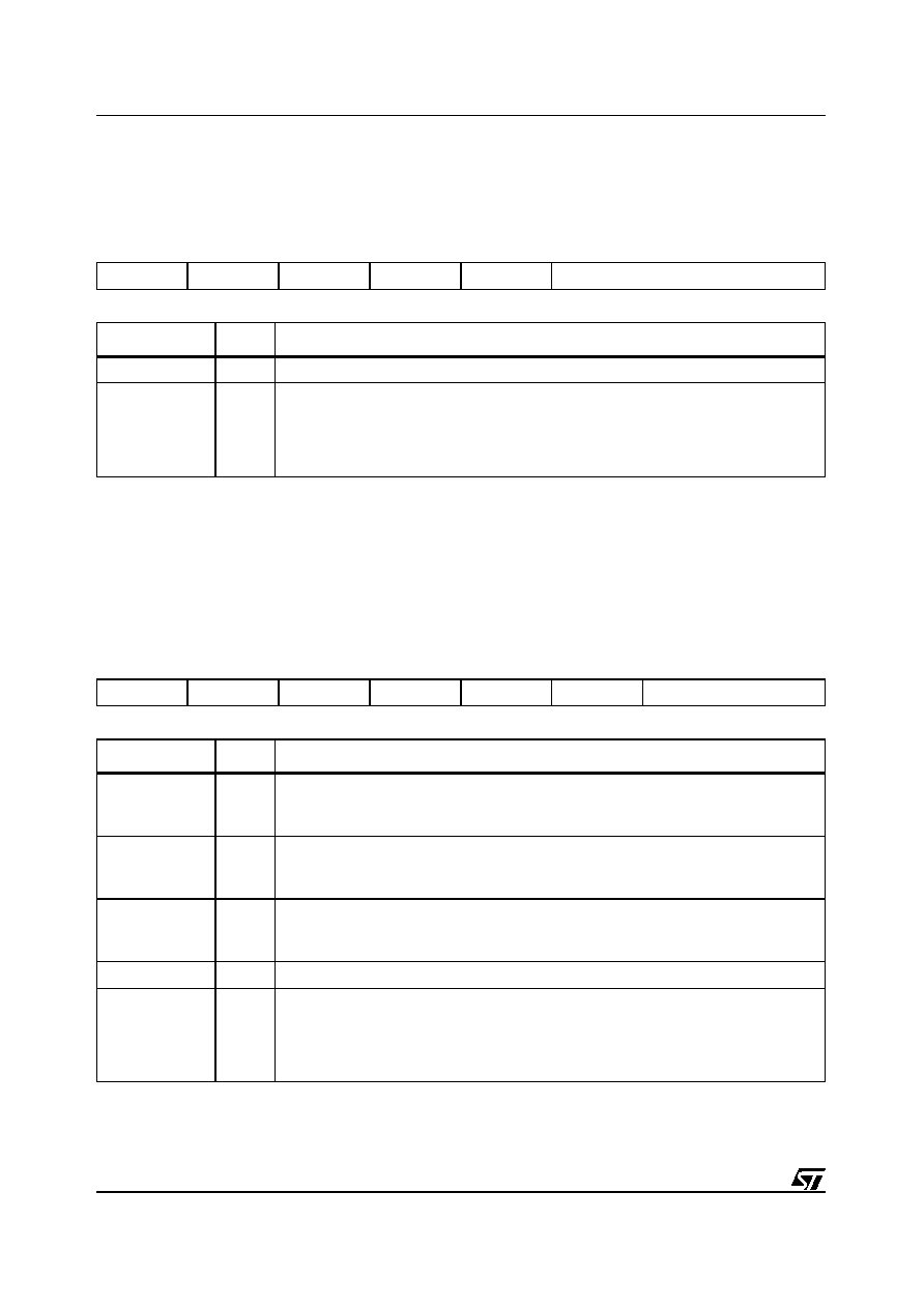
Register List
STV82x6
80/97
SW_BAND
Subwoofer Bandwidth Control
9.18
Beeper
BEEPER_CTRL
Beeper Control
Address (hex): 6Bh
Type: R/W
Bit 7
Bit 6
Bit 5
Bit 4
Bit 3
Bit 2
Bit 1
Bit 0
0
0
0
0
SW_FREQ[2:0]
Bit Name
Reset
Function
Bits[7:3]
00000
Reserved.
SW_FREQ[2:0]
011
Cut-off frequency tuning from 50 Hz to 400 Hz in steps of 50 Hz
000: 50 Hz
100: 250 Hz
001: 100 Hz
101: 300 Hz
010: 150 Hz
110: 350 Hz
011: 200 Hz (Default)
111: 400 Hz
Address (hex): 79h
Type: R/W
Bit 7
Bit 6
Bit 5
Bit 4
Bit 3
Bit 2
Bit 1
Bit 0
LS_BEEP_ON HP_BEEP_ON BEEP_MODE
0
0
0
BEEP_DURATION[1:0]
Bit Name
Reset
Function
LS_BEEP_ON
0
Loudspeaker Beeper Enable
0: Loudspeaker beeper muted (Default)
1: Loudspeaker beeper enabled (Start pulse and automatic reset in Pulse mode)
HP_BEEP_ON
0
Headphone Beeper Enable
0: Headphone beeper muted (Default)
1: Headphone beeper enabled (Start pulse and automatic reset in Pulse mode)
BEEP_MODE
0
Beeper Mode Select
0: Pulse mode (for Beep applications - Default)
1: Continuous mode (for Alarm application)s
Bit[4:0]
000
Reserved.
BEEP_DURATION[
1:0]
00
Defines the duration of the beeper (for Pulse mode only).
00: 0.128 s
01: 0.256 s.
10: 0.512 s.
11: 1.024 s.
81/97
STV82x6
Register List
BEEPER_TONE
Beeper Tone Control
Address (hex): 7Ah
Type: R/W
Bit 7
Bit 6
Bit 5
Bit 4
Bit 3
Bit 2
Bit 1
Bit 0
BEEP_FREQ[2:0]
BEEP_VOL[4:0]
Bit Name
Reset
Function
BEEP_FREQ[2:0]
011
Defines the frequency of the beeper tone from 62.5 Hz to 8 kHz in octaves
000: 62.5 Hz
100: 1 kHz
001: 125 Hz
101: 2 kHz
010: 250 Hz
110: 4 kHz
011: 500 Hz (Default)
111: 8 kHz
BEEP_VOL[4:0]
10000
Defines the Beeper volume from 0 to -93 dB in steps of 3 dB.
11111: 0 dB (1 V
RMS
)
...
11110: -3 dB
00011: -84 dB
11101: -6 dB
00010: -87 dB
...
00001: -90 dB
10000: -48 dB (Default)
00000: -93 dB
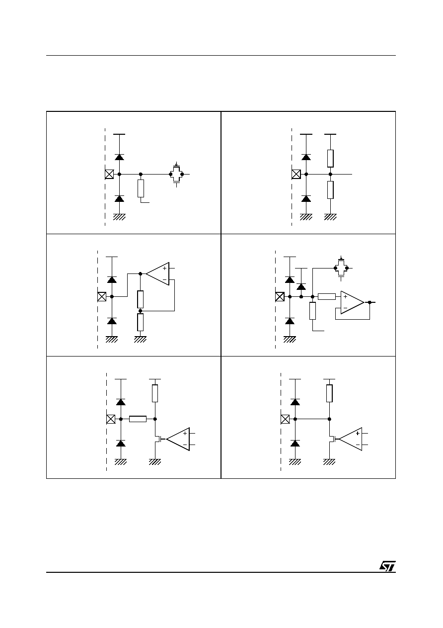
Input/Output Groups
STV82x6
82/97
10
Input/Output Groups
Pin numbers apply to SDIP package only.
VDDH
5K
GNDIF
VREFIF
1
SIF
VDDH
500
GNDIF
2
VTOP
160
VDDIF
VDDH
6K
GNDIF
3
VREFIF
30K
BGAP(1.2V)
VDDH
400
GNDIF
6
MONOIN
22K
VREFIF
VDDA
VDDH
300
GNDA
8
AO1R
2K
19
AO2L
20
AO2R
7
AO1L
VDDH
GNDA
VDDH
GNDA
27
LSR
2K
28
SW
29
HPL
26
LSL
VDDH
GNDA
30
HPR
83/97
STV82x6 Input/Output
Groups
VDDH
GNDA
11
AI1L
12
AI1R
GNDA
15
AI2L
16
AI2R
23
AI3L
24
AI3R
40K
90K
47K
82K
VDDH
GNDA
13
VMC1
200
BGAP
6K
30K
(1.2V)
VDDH
6K
GNDA
14
VMC2
30K
BGAP
(1.2V)
VDDH
3K
GNDA
15K
22
VREFA
BGAP
(1.2V)
VDDH
GNDA
25
BGAP
10K
BAND-GAP=1.2V
GNDA
76
9
VDDC
BGAP
(1.2V)
Input/Output Groups
STV82x6
84/97
VDDH
VDDC
VDDIF
GNDA
GNDIF
GNDC
GNDS
18
21
4
9
5
10
31
17
VDDA
76
17
VDDA
GNDA
18
BGAP
(1.2V)
1.2K
8K
BGAP
(1.2V)
40
VDD1
47
36
REG
41
48
VDD2
GND1
GND2
GND1
32
HPD
33
37
ADR
RESET
GND2
50
SDO
51
ST
52
WS
53
SCK
54
BUS1
55
BUS0
56
IRQ
VDD2
6
GND1
39
MCK
VDD1
6
GND1
38
SYSCK
VDD1
3
GND1
34
SCL
12
35
SDA
85/97
STV82x6 Input/Output
Groups
44
XTO
GNDP
43
XTI
VDDP
Electrical Characteristics
STV82x6
86/97
11
Electrical Characteristics
A 10 k
load is applied to all outputs.
11.1
Absolute Maximum Ratings
Note:
Analog supply voltages (V
DDIF
, V
DDC
and V
DDA
) are regulated by internal circuits. For more
information, refer to
Section 7.1: Supply Voltages
.
11.2
Thermal Data
11.3
Supply
Test Conditions: T
OPER
= 25∞ C, V
DDH
= 8 V, V
DDA
is supplied by 8 V via 330
, V
DDIF
is connected
to V
DDC
and is supplied by 5 V via 22
and DV
DD
(V
DD1
, V
DD2
and V
DDP
) is supplied by 5 V via an
external ballast transistor. For more information, refer to
Figure 4 on page 7
.
Symbol
Parameter
Value
Units
DV
DD
Digital Supply Voltage (V
DD1
, V
DD2
, V
DDP
)
4.6
V
HV
DD
Analog Supply High Voltage (V
DDH
)
9.5
V
V
ESD
Capacitor 100 pF discharged via 1.5 k
serial resistor (Human Body Model)
±4
kV
T
OPER
Operating Ambient Temperature
0, +70
∞C
T
STG
Storage Temperature
-55 to +150
∞C
Symbol
Parameter
Value
Units
R
thJA
Junction-to-Ambient Thermal Resistance
SDIP56
TQFP80
40
42
∞C/W
Symbol
Parameter
Test Conditions
Min.
Typ.
Max.
Units
DV
DD
Digital Supply Voltage (V
DD1
, V
DD2
, V
DDP
)
3.0
3.3
3.6
V
HV
DD
Analog Supply High Voltage (V
DDH
)
7.6
8.0
8.4
V
AV
DD
Analog Supply Voltage (V
DDIF
, V
DDC
, V
DDA
)
3.0
3.3
3.6
V
I
VDD
V
DD
Current Consumption (V
DD1
, V
DD2
, V
DDP
)
130
160
190
mA
I
VDDIF
I
VDDC
V
DDIF
Current Consumption (V
DDIF
, V
DDC
)
60
75
85
mA
I
VDDA
V
DDA
Current Consumption
7
12
18
mA
I
VDDH
V
DDH
Current Consumption
5.0 V
15
mA
8.0 V
15
25
35
87/97
STV82x6 Electrical
Characteristics
11.4
Crystal Recommendations
11.5
Analog Sound IF Signal Recommendations
Symbol
Parameter
Min.
Typ.
Max. Units
F
P
Crystal Parallel Resonance Frequency (at 22 pF load capacitor)
27
MHz
DF/F
P
Frequency Tolerance at 25 ∞C
-50
+50
ppm
DF/F
T
Frequency Stability versus Temperature within a range from 0 to 70 ∞C
-50
+50
ppm
C1
Motional Capacitor
8
fF
R
S
Serial Resistance
50
C
S
Shunt Capacitance
7
pF
Symbol
Parameter
Test Conditions
Min.
Typ.
Max.
Units
F
SIF
SIF Carrier Frequency
4
8
MHz
R
INSIF
SIF Input Resistance
4.5
6
7.5
k
DC
INSIF
SIF Input DC Level
1.47
V
C
INSIF
SIF Input Capacitance
15
pF
FM Carrier
VSIF
FM
SIF Input Level for FM Carrier
0.02
1.6
V
PP
DEV
FM
FM Deviation
FM50k (Standard)
±15
±50
±125
kHz
FM200k (DK only)
±200
FM350k (DK only)
±350
FM500k (DK mono only)
±500
DFSIF
FM
SIF Carrier Accuracy for FM
Standard (FM50k)
±1
±5
kHz
Shifted Standard (FM50k with
DCO compensation)
±120
kHz
R
FM1/FM2
Carrier Ratio FM1/FM2 for A2 System
7
dB
R
FM/QPSK
Carrier Ratio FM/QPSK for NICAM System
13
dB
AM Carrier
VSIF
AM
SIF Input Level for AM Carrier (Unmodulated)
0.04
0.8
V
PP
DEV
AM
Modulation Depth for AM
0
100
%
DFSIF
AM
SIF Carrier Accuracy for AM
±1
±5
kHz
R
AM/QPSK
AM/QPSK Carrier Ratio for NICAM System
17
dB
Electrical Characteristics
STV82x6
88/97
11.6
SIF to LS/HP/SCART Path Characteristics
11.7
SCART to SCART Analog Path Characteristics
Symbol
Parameter
Test Conditions
Min.
Typ.
Max.
Units
FM Demodulation
BAND
FM
Frequency Response
20Hz - 15kHz
-1.5
+1.5
dB
SNR
FM
Signal to Noise
RMS unweighted, 20Hz-15kHz,
Standard B/G 50 kHz FM Deviation,1kHz
LS Output 0.7 V
RMS
70
dB
THD
FM
Total Harmonic Distortion
0.1
%
SEP
FM
Stereo Channel Separation
RMS
Standard B/G stereo A2, 50 kHz FM
deviation, 1 kHz
45
dB
XTALK
FM
Dual Channel Crosstalk
RMS
Standard B/G dual mono A2, 50 kHz FM
deviation, 1 kHz
80
dB
NICAM Demodulation
BAND
NIC
Frequency Response
20Hz - 15kHz
-1.0
+1.0
dB
SNR
NIC
Signal to Noise
RMS unweighted, 20Hz-15kHz,
Standard B/G mono NICAM,1 kHz
LS Output 0.7 V
RMS
72
dB
THD
NIC
Total Harmonic Distortion
0.1
%
SEP
NIC
Stereo Channel Separation
RMS
Standard B/G stereo NICAM, 1 kHz
80
dB
XTALK
NIC
Dual Channel Crosstalk
RMS
Standard B/G dual mono NICAM, 1 kHz
80
dB
AM Demodulation
BAND
AM
Frequency Response
20 Hz - 15 kHz
-1.0
+1.0
dB
SNR
AM
Signal to Noise
RMS unweighted 2 0Hz-15 kHz,
Standard L, 54% AM Depth, 1 kHz
LS Output 0.7 V
RMS
50
dB
THD
AM
Total Harmonic Distortion
0.6
%
Symbol
Parameter
Test Conditions
Min.
Typ.
Max.
Units
Analog-to-Analog (Through mode)
R
INSCART
SCART Input Resistance
24
30
40
k
R
OUTSCART
Output Resistance for SCARTs
250
300
450
VDC
INSCART
SCART Input DC Level
2.55
V
VDC
OUTSCART
SCART Output DC Level
VDDH = 5 V
VDDH = 8 V
2.20
3.40
V
Clipping
THD
V
IN
= 2 V
RMS
at 1 kHz for VDDH = 8 V
0.1
0.5
%
THD
Total Harmonic Distortion
V
IN
= 1.00 V
RMS
at 1 kHz for VDDH = 5 V
V
IN
= 1.75 V
RMS
at 1 kHz for VDDH = 8 V
0.0125
0.0125
0.03
0.05
%
89/97
STV82x6 Electrical
Characteristics
11.8
SCART to I2S Output Path (via ADC) Characteristics
11.9
MONOIN to ADC and I2S Output Path Characteristics
11.10 I2S to LS/HP/SW Path Characteristics
SNR
Signal to Noise Ratio
20 to 20 kHz Bandwidth, RMS unweighted
V
IN
= 1.00 V
RMS
for VDDH = 5 V
V
IN
= 1.75 V
RMS
for VDDH = 8 V
75
80
85
90
dB
BAND
Frequency Response
20 Hz to 20 kHz
-0.5
0.5
dB
XTALK
L/R
Left/Right Crosstalk
1.4 V
RMS
@ 1 kHz on ref signal, the other
one grounded
70
75
dB
XTALK
IN1/2
Audio Crosstalk from Input
Channel 1 to Input Channel 2
1.4 V
RMS
@ 1 kHz on ref signal, all other
inputs grounded
80
85
dB
XTALK
OUT1/2
Audio Crosstalk from Output
Channel 1 to Output Channel 2
1.4 V
RMS
@ 1 kHz on reference output,
signal on a single input, all other inputs
grounded
80
85
dB
Symbol
Parameter
Test Conditions
Min.
Typ.
Max.
Units
Clipping
THD
V
IN
= 1 V
RMS
at 1 kHz for VDDH = 5 V
V
IN
= 2 V
RMS
at 1 kHz for VDDH = 8 V
0.5
0.2
2.0
2.0
%
THD
Total Harmonic Distortion
V
IN
= 0.90 V
RMS
at 1 kHz for VDDH = 5 V
V
IN
= 1.75 V
RMS
at 1 kHz for VDDH = 8 V
0.03
0.03
0.05
0.05
%
SNR
Signal to Noise Ratio
20 to 15 kHz Bandwidth, RMS unweighted
V
IN
= 0.90 V
RMS
for VDDH = 5 V
V
IN
= 1.75 V
RMS
for VDDH = 8 V
70
70
74
74
dB
BAND
Frequency Response
20 Hz to 15 kHz
-0.5
0.5
dB
Symbol
Parameter
Test Conditions
Min.
Typ.
Max.
Units
R
INMONOIN
MONO Input Resistance
15
22
30
k
VDC
INMONOIN
MONO Input DC Level
1.45
V
THD
Total Harmonic Distortion
V
IN
= 0.45 V
RMS
at 1 kHz
0.03
0.05
%
SNR
Signal to Noise Ratio
20 to 15 kHz Bandwidth, RMS unweighted
V
IN
= 0.45 V
RMS
70
74
dB
BAND
Frequency Response
20 Hz to 15 kHz
-0.5
0.5
dB
Symbol
Parameter
Test Conditions
Min.
Typ.
Max.
Units
R
OUTMAIN
Output Resistance for Main
Outputs
LSL, LSR, SW, HPL and HPR pins
5
30
VDC
OUTMAIN
MAIN Output DC Level
2.20
V
Symbol
Parameter
Test Conditions
Min.
Typ.
Max.
Units
Electrical Characteristics
STV82x6
90/97
11.11 I2S to SCART Path Characteristics
11.12 Loudspeaker and Headphone Volume Control Characteristics
11.13 MUTE Performance
11.14 Digital I/Os
THD
Total Harmonic Distortion
90% Full-scale Range at 1 kHz
0.025
0.050
%
SNR
Signal to Noise Ratio
20 to 15 kHz Bandwidth, RMSunweighted,
90% Full-scale Range
72
76
dB
V
OUTAMP
MAIN Output Amplitude
90% Full-scale Range at 1 kHz
0.800
0.875
0.950
V
RMS
Symbol
Parameter
Test Conditions
Min.
Typ.
Max.
Units
THD
Total Harmonic Distortion
90% Full-scale Range at 1 kHz
0.025
0.100
%
SNR
Signal to Noise Ratio
20 Hz to 15 kHz Bandwidth unweighted,
90% Full-scale Range
72
76
dB
V
OUTAMP
MAIN Output Amplitude
90% Full-scale Range at 1 kHz, VDDH = 8V
1.60
1.75
1.90
V
RMS
Symbol
Parameter
Test Conditions
Min.
Typ.
Max.
Units
VOL_MIN
Maximum Attenuation
I2S to DAC at 1 kHz with 1 active channel
82
90
dB
VOL_DNL
Maximum Non-Linearity Step to
Step
Volume Control Range of 0 dB to 72 dB
0.1
0.3
dB
Symbol
Parameter
Test Conditions
Min.
Typ.
Max.
Units
DAC Mute
I2S to DAC at 1 kHz with 1 active channel
85
95
SCART Mute
1.4 V
RMS
@ 1 kHz on ref signal, all other
inputs grounded
78
81
Symbol
Parameter
Test Conditions
Min.
Typ.
Max.
Units
V
IL
Low Level Input Voltage
0.5
V
V
IH
High Level Input Voltage
2.0
V
I
IN
Input Current
1
µA
Symbol
Parameter
Test Conditions
Min.
Typ.
Max.
Units
91/97
STV82x6 Electrical
Characteristics
11.15 I≤C Bus Interface
Symbol
Parameter
Min.
Typ.
Max.
Units
SCL
V
IL
Input Voltage Low Level
0
0.7
V
V
IH
Input Voltage High Level
3
V
DD
V
V
OL
Low Output Voltage (I
OL
= 3 mA)
0
0.8
V
f
SCL
SCL Clock Frequency
400
kHz
t
r
, t
f
Input Rise/Fall Times (10 to 90%)
0.8
µs
I
I(L)
Input Leakage Current (V
I
= 5.5 V)
10
µA
C
l
Input Capacitance
10
pF
SDA
V
IL
Input Voltage Low Level
0
0.7
V
V
IH
Input Voltage High Level
3
V
DD
V
t
r
, t
f
Input Rise/Fall Times (10 to 90%)
0.8
µs
I
I(L)
Input Leakage Current (V
I
= 5.5 V with Output Off)
10
µA
V
OL
Low Output Voltage (I
OL
= 3 mA)
0
0.8
V
t
fo
Output Fall Time between 3 V and 1 V
0.6
µs
C
L
Load Capacitance
400
pF
I
ACK
Maximum Sink Current
3
mA
TIMING
t
LOW
Low Period
1
µs
t
HIGH
High Period
1
µs
t
SU, DAT
Data Setup Time
250
ns
t
HD, DAT
Data Hold Time
250
ns
t
SU, STOP
Stop Setup Time from Clock High
1
µs
t
BUF
Start Setup Time following a Stop
1
µs
t
HD, STA
Start Hold Time
1
µs
t
SU, STA
Start Setup Time following Clock Low to High Transition
1
µs
Electrical Characteristics
STV82x6
92/97
Figure 19: Serial Bus Timing
t
hd, sta
t
low
t
r
t
buf
t
high
t
f
t
su, dat
SDA
SCL
SDA
for Start
and Stop
t
su, sta
t
su, sto
t
hd, dat
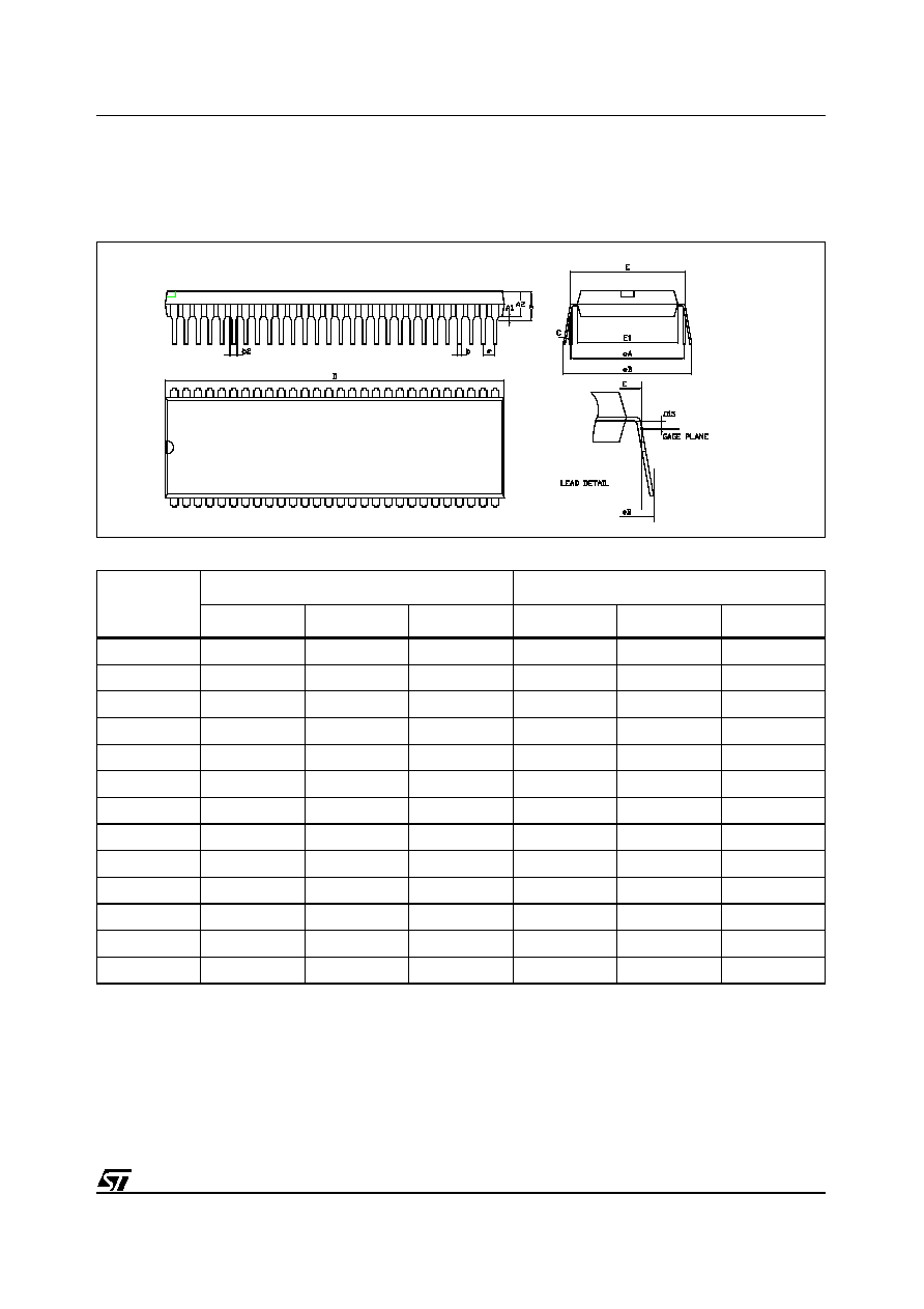
93/97
STV82x6
Package Mechanical Data
12
Package Mechanical Data
Figure 20: 56-Pin Shrink Plastic Dual In Line Package, 600-mil Width
Dim.
mm
inches
A
6.35
0.250
A1
0.38
0.015
A2
3.18
4.95
0.125
0.195
b
0.41
0.016
b2
0.89
0.035
C
0.20
0.38
0.008
0.015
D
50.29
53.21
1.980
2.095
E
15.01
0.591
E1
12.32
14.73
0.485
0.580
e
1.78
0.070
eA
15.24
0.600
eB
17.78
0.700
L
2.92
5.08
0.115
0.200
SDIP56
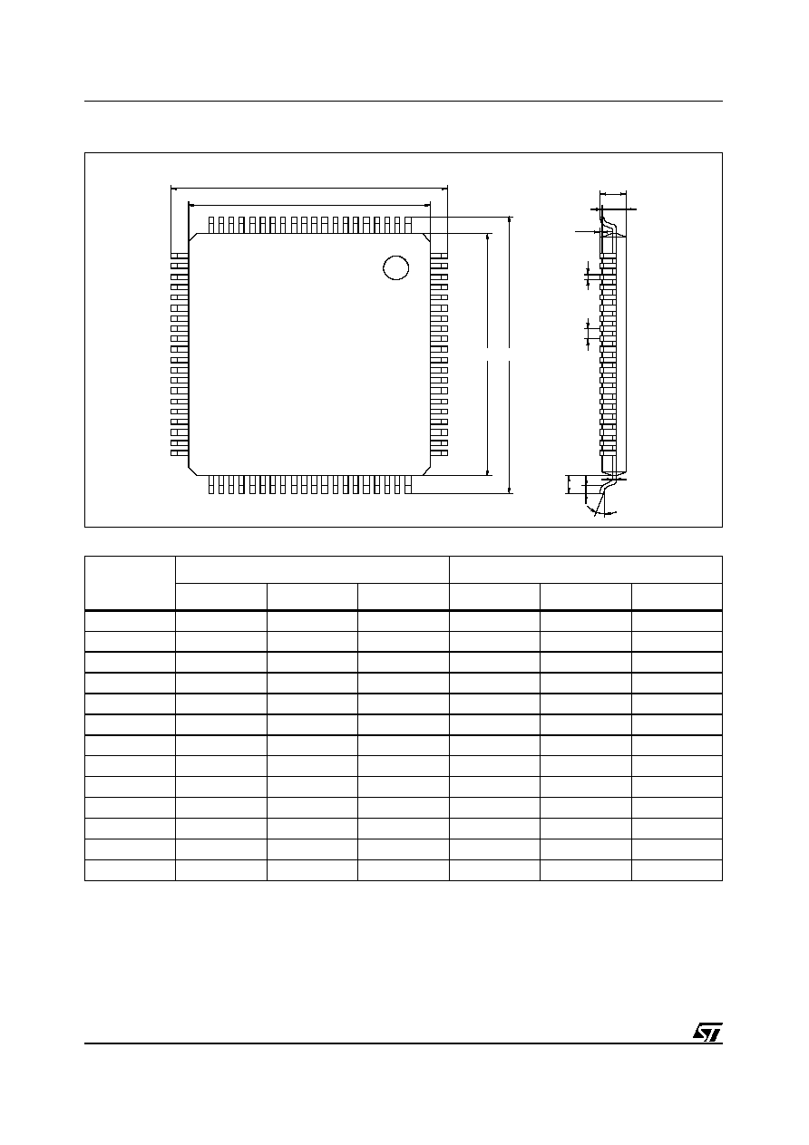
Package Mechanical Data
STV82x6
94/97
Figure 21: 80-Pin Thin Plastic Quad Flat Package
Dim.
mm
inches
Min.
Typ.
Max.
Min.
Typ.
Max.
A
1.60
0.063
A1
0.05
0.15
0.002
0.006
A2
1.35
1.40
1.45
0.053
0.055
0.057
b
0.22
0.32
0.38
0.009
0.013
0.015
C
0.09
0.20
0.004
0.008
D
16.00
0.630
D1
14.00
0.551
E
16.00
0.630
E1
14.00
0.551
e
0.65
0.026
K
0∞
3.5∞
0.75∞
0∞
3.5∞
0.75∞
L
0.45
0.60
0.75
0.018
0.024
0.030
L1
1.00
0.039
A
A2
A1
b
e
h
c
L
L1
E
E1
D1
D
95/97
STV82x6 Revision
History
13
Revision History
Date
Revision
Modification
10 Jan 2003
2.0
First Release
7 May 2003
2.1
Modification to
Table 6: Volume/Balance Control Registers on page 21
.
14 May 2004
2.2
Addition of pin 12 (TQFP80) to
Table 2
. Updated
Figure 6
.
25 Feb 2005
3
Modification of CETH (20h) register recommended value.
STV82x6
96/97
Index
A
Analog Power Supply ........................................ 29
Analog-to-Digital Conversion ............................. 12
Automatic Frequency Control ............................ 14
Automatic Gain Control ...................................... 12
Automatic Overmodulation Detection ................ 13
Automatic Standard Recognition System 12-13, 33
B
Balance Control ................................................. 20
Bass Control ...................................................... 19
Beeper ............................................................... 22
C
Clock .................................................................. 16
Clock System Output ......................................... 28
D
Digital Power Supply .......................................... 29
Digital Stereo Output ......................................... 28
H
Headphone Detection Mode .............................. 21
I
I2C Address ....................................................... 31
I2S ..................................................................... 28
Independent Mute Control ................................. 21
Input Audio Matrixing ......................................... 26
L
Loudness Control .............................................. 22
M
Mute Control ...................................................... 21
O
Output Audio Matrixing ...................................... 26
P
Peak Detector .................................................... 13
Peak Level Detector .......................................... 26
Philips Mode ...................................................... 28
Power Supplies .................................................. 29
S
Signal to Noise ................................................... 88
Smart Volume Control ....................................... 18
Sony Mode ......................................................... 28
Sound IF Signal ................................................. 12
SRS 3D Surround .............................................. 23
ST Wide Surround ............................................. 19
Stereo Flag ........................................................ 27
Supply Voltages ................................................. 29
T
Total Harmonic Distortion .................................. 88
Treble Control .................................................... 19
V
Voltage Regulator .............................................. 29
Volume Control .................................................. 20
W
Word Selection Polarity ..................................... 28

STV82x6
97/97
Information furnished is believed to be accurate and reliable. However, STMicroelectronics assumes no responsibility for the
consequences of use of such information nor for any infringement of patents or other rights of third parties which may result
from its use. No license is granted by implication or otherwise under any patent or patent rights of STMicroelectronics.
Specifications mentioned in this publication are subject to change without notice. This publication supersedes and replaces
all information previously supplied. STMicroelectronics products are not authorized for use as critical components in life
support devices or systems without express written approval of STMicroelectronics.
The ST logo is a registered trademark of STMicroelectronics
All other names are the property of their respective owners
© 2005 STMicroelectronics - All rights reserved
STMicroelectronics GROUP OF COMPANIES
Australia - Belgium - Brazil - Canada - China - Czech Republic - Finland - France - Germany - Hong Kong - India - Israel - Italy
- Japan - Malaysia - Malta - Morocco - Singapore - Spain - Sweden - Switzerland - United Kingdom - United States
www.st.com