 | –≠–ª–µ–∫—Ç—Ä–æ–Ω–Ω—ã–π –∫–æ–º–ø–æ–Ω–µ–Ω—Ç: STV9212 | –°–∫–∞—á–∞—Ç—å:  PDF PDF  ZIP ZIP |
This is preliminary information on a new product now in development or undergoing evaluation. Details are subject to change without notice.
October 2003
1/34
Æ
STV9212
Video Processor for CRT Monitors with PictureBooST
TM
Main Features
s
General
q
I≤C-Bus Controlled
q
Supports AC- and DC-coupled applications
q
5V to 8V Power Supply
q
Matches to virtually any video amplifier
s
PictureBooST
TM
q
PictureBooST
TM
insertion input
q
Full-screen PictureBooST
TM
via I≤C-bus
q
Context-sensitive Picture Enhancement
s
Video Clamping
q
Input and Output Video Clamp
q
Sync Pulse Polarity Auto-rectification
q
Clamp Pulse Generation timed either by sync
or video blanking pulse
s
Video Processing
q
Contrast Adjustment with excellent channel
matching
q
Gain stages for control of white
q
Two DC-mode cut-off ranges
q
Output DC offset control
q
Automatic Beam Limiter (ABL)
q
Video Insertion Pulse (VIP), 2 levels
q
Amplifier Control (Blanking and Stand-by)
s
OSD Insertion with Contrast Control
s
Control Output
q
Amplifier Standby and Blanking Control
q
3 DAC for control of DC Restore Amplifier or
Brightness in DC-coupled system
General Description
The STV9212 is an I≤C-bus controlled color video
processor designed for standard CRT monitor
applications. It can drive systems where cathodes
are either AC- or DC-coupled to the amplifier
outputs. The three video channels provide contrast
and white balance separate gain adjustments as
well as one-per-channel DC cut-off control and
common DC offset control functions. On top of
these usual controls, it features context-sensitive
picture enhancement circuitry to support the
PictureBooST
TM
function that enhances the
appearance of still pictures and moving video.
In AC coupling applications, the device can pilot
three cathode DC restore channels dedicated to set
CRT cut-off bias voltages and to control brightness
through cathodes.
The RGB video outputs have a class A architecture
and directly drive the amplifier channels without
unnecessarily consuming current. Bandwidth
limitation I≤C-bus adjustments can contribute to
keeping the application EMI under control.
OSD (On-Screen Display) graphics are inserted by
means of a Fast Blanking signal. Independent OSD
contrast control facilitates adaptation to various
OSD generators and provides system flexibility.
The STV9212 is perfectly compatible with other ST
components for CRT video boards, such as video
amplifiers and OSD generators.
DIP24S:(Plastic Package)
ORDER CODE: STV9212

STV9212
2/34
Table of Contents
Chapter 1
STV9212 Pin Allocation and Description . . . . . . . . . . . . . . . . . . . . . . . . . . . . . . .4
1.1
Pinout .................................................................................................................................. 4
1.2
Pin Descriptions .................................................................................................................. 4
Chapter 2
Functional Description . . . . . . . . . . . . . . . . . . . . . . . . . . . . . . . . . . . . . . . . . . . . .5
2.1
Video RGB Input Clamp ....................................................................................................... 6
2.2
Video Blanking ..................................................................................................................... 8
2.3
Contrast Control Stage and Automatic Beam Limiter .......................................................... 9
2.4
PictureBooST ..................................................................................................................... 10
2.5
OSD Insertion ..................................................................................................................... 11
2.6
Drive Stage ........................................................................................................................ 11
2.7
Video Insertion Pulse ......................................................................................................... 12
2.8
Output Stage ...................................................................................................................... 12
2.9
Output Infra-black Level, Cut-off and Brightness ............................................................... 15
2.10
Signal Waveforms .............................................................................................................. 18
2.11
Miscellaneous .................................................................................................................... 18
Chapter 3
I≤C-Bus Interface Specifications . . . . . . . . . . . . . . . . . . . . . . . . . . . . . . . . . . . . .20
3.1
I≤C-bus Register Descriptions ............................................................................................ 21
Chapter 4
Electrical Specifications . . . . . . . . . . . . . . . . . . . . . . . . . . . . . . . . . . . . . . . . . . .24
4.1
Absolute Maximum Ratings ............................................................................................... 24
4.2
Thermal Data ..................................................................................................................... 24
4.3
Static Electrical Characteristics .......................................................................................... 24
4.4
Dynamic Electrical Characteristics ..................................................................................... 25
4.5
I≤C-Bus Electrical Characteristics ....................................................................................... 27
4.6
I≤C-Bus Interface Timing Requirements ........................................................................... 27
Chapter 5
Soldering Information . . . . . . . . . . . . . . . . . . . . . . . . . . . . . . . . . . . . . . . . . . . . .29
Chapter 6
Package Mechanical Data . . . . . . . . . . . . . . . . . . . . . . . . . . . . . . . . . . . . . . . . .30
Chapter 7
Input/Output Diagrams . . . . . . . . . . . . . . . . . . . . . . . . . . . . . . . . . . . . . . . . . . . .31

3/34
STV9212
Chapter 8
Revision History . . . . . . . . . . . . . . . . . . . . . . . . . . . . . . . . . . . . . . . . . . . . . . . . . .33
STV9212 Pin Allocation and Description
STV9212
4/34
1
STV9212 Pin Allocation and Description
1.1
Pinout
1.2
Pin Descriptions
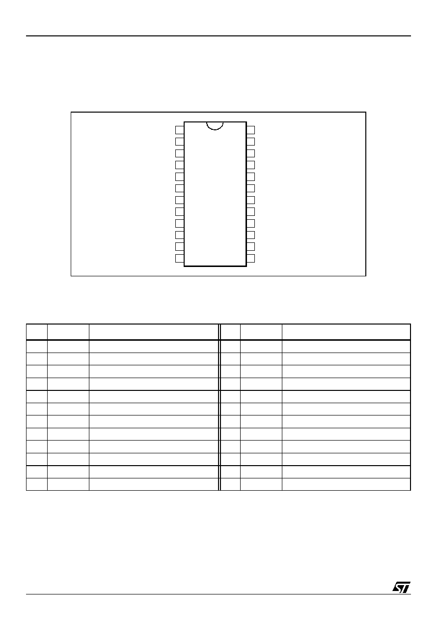
Figure 1: STV9212 Pinout
Table 1: STV9212 Pin Descriptions
Pin
Name
Function
Pin
Name
Function
1
IN1
Video Input, Channel 1
13
SCL
I≤C-bus Clock Input
2
HS
Video Clamp Sync Input
14
SDA
I≤C-bus Data Input/Output
3
IN2
Video Input, Channel 2
15
CO3
Cut-off / Brightness DAC 3 Output
4
ABL
Automatic Beam Limiter Input
16
CO2
Cut-off DAC 2 Output
5
IN3
Video Input, Channel 3
17
CO1
Cut-off DAC 1 Output
6
GNDA
Analog Ground
18
OUT3
Video Output, Channel 3
7
VCCA
Analog Supply
19
GNDP
Output Stage Ground
8
PB
Picture Boost Input
20
OUT2
Video Output, Channel 2
9
OSD1
OSD Input, Channel 1
21
VCCP
Output Stage Supply
10
OSD2
OSD Input, Channel 2
22
OUT1
Video Output, Channel 1
11
OSD3
OSD Input, Channel 3
23
AMPCTL
Output for Amplifier Control
12
FBLK
OSD Insertion Control Input
24
BLK
Blanking and Video Clamp Sync Input
1
2
3
4
5
6
7
8
9
10
15
16
24
23
22
21
20
19
18
17
11
14
12
13
IN1
HS
IN2
ABL
IN3
GNDA
VCCA
PB
OSD1
OSD2
OSD3
FBLK
BLK
AMPCTL
OUT1
VCCP
OUT2
GNDP
OUT3
CO1
CO2
CO3
SDA
SCL
5/34
STV9212
Functional Description
2
Functional Description
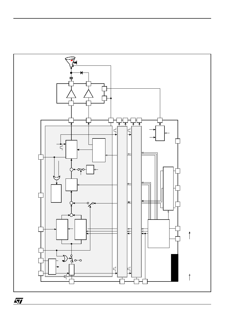
The functional blocks are described in the order they act on the signal.
Figure 2: STV9212 Block Diagram
BL
K
HS
V
CCP
FB
L
K
SD
A
S
C
L
14
13
O
S
D1
O
S
D2
O
S
D3
6
GN
D
A
20
OU
T
2
18
OU
T
3
3
5
4
IN
1
IN
2
IN
3
ABL
23
AM
P
C
T
L
ST
V9
2
1
2
Vr
e
f
1
OU
T
1
+
GN
D
P
I
≤C
3V
(
D
C
)
P
r
e
A
mp
lif
i
e
r
S
t
a
nd-
by
EH
T
A
m
p
lif
ie
r
GN
D
ST
D
B
/
Dri
v
e
2
24
21
O
u
t
put
C
hannel
1
DC
o
r
A
C
22
G
V
Sta
g
e
12
FB
L
K
17
G
DC
7
VC
C
A
PB
8
CO
1
DC
I
N
1
DC
O
U
T
1
19
16
CO
2
15
CO
3
I≤
C
BL
K
IC
P
,
O
C
P
9
10
11
VO
U
T
1
D
e
c
ode
r
I≤
C
-
b
u
s
S
t
an
db
y
&
Bl
a
n
k
i
n
g
I≤
C
VC
C
P
BL
K
I
BL
K
I
I≤
C
I
≤
C-
bus
c
o
nt
rol
pa
t
h
v
i
de
o/
c
o
nt
ro
l
s
i
gna
l
p
a
t
h
Cl
am
p
BL
KI
IC
P
IC
P
+
BL
KI
OC
P
OC
P
OS
D
I
n
f
r
a-
bl
ac
k
l
e
v
e
l
cu
t-
o
f
f
B
r
i
g
ht
ne
s
s
VIP
le
v
e
l
C
hannel
3
O
S
D Co
nt
ra
st
C
hannel
2
+
Co
nt
ras
t
P
i
c
t
ur
e
B
oo
S
T