 | –≠–ª–µ–∫—Ç—Ä–æ–Ω–Ω—ã–π –∫–æ–º–ø–æ–Ω–µ–Ω—Ç: STV9302 | –°–∫–∞—á–∞—Ç—å:  PDF PDF  ZIP ZIP |
September 2003
1/15
Æ
STV9302A
Vertical Deflection Booster
for 2-A
PP
TV/Monitor Applications with 70-V Flyback Generator
Main Features
s
Power Amplifier
s
Flyback Generator
s
Output Current up to 2 App
s
Thermal Protection
s
Stand-by Control
Description
The STV9302A is a vertical deflection booster
designed for TV and monitor applications.
This device, supplied with up to 35 V, provides up to
2 App output current to drive the vertical deflection
yoke.
The internal flyback generator delivers flyback
voltages up to 70 V.
in double-supply applications, a stand-by state will
be reached by stopping the (+) supply alone.
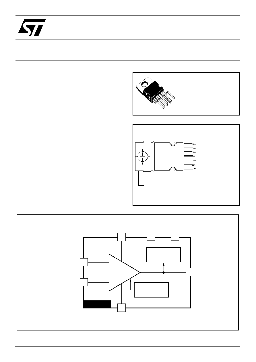
HEPTAWATT
(Plastic Package)
ORDER CODE: STV9302A
7
6
5
4
3
2
1
Tab connected
Input (Non Inverting)
Output Stage Supply
Output
Ground Or Negative Supply
Flyback Generator
Supply Voltage
Input (Inverting)
to pin 4
1
Thermal
Protection
6
4
3
5
STV9302A
+
-
Power
Amplifier
7
2
Flyback
Generator
Inverting
Non-Inverting
Input
Input
Ground or Negative Supply
Output
Flyback
Generator
Output Stage
Supply
Voltage
Supply
Absolute Maximum Ratings
STV9302A
2/15
1
Absolute Maximum Ratings
Note:1. Usually the flyback voltage is slightly more than 2 x V
S
. This must be taken into consideration when
setting
V
S.
2. Versus pin 4
3. V3 is higher than V
S
during the first half of the flyback pulse.
4. Such repetitive output peak currents are usually observed just before and after the flyback pulse.
5. This non-repetitive output peak current can be observed, for example, during the Switch-On/Switch-
Off phases. This peak current is acceptable providing the SOA is respected (
Figure 8
and
Figure 9
).
6. All pins have a reverse diode towards pin 4, these diodes should never be forward-biased.
7. Input voltages must not exceed the lower value of either V
S
+ 2 or 40 volts.
2
Thermal Data
Symbol
Parameter
Value
Unit
Voltage
V
S
Supply Voltage (pin 2) -
Note 1
and
Note 2
40
V
V
5
, V
6
Flyback Peak Voltage -
Note 2
70
V
V
3
Voltage at Pin 3 -
Note 2
,
Note 3
and
Note 6
-0.4 to (V
S
+ 3)
V
V
1
, V
7
Amplifier Input Voltage -
Note 2
,
Note 6
and
Note 7
- 0.4 to (V
S
+ 2) or +40
V
Current
I
0
(1)
Output Peak Current at f = 50 to 200 Hz, t
10µs -
Note 4
±5
A
I
0
(2)
Output Peak Current non-repetitive -
Note 5
±2
A
I
3
Sink
Sink Current, t<1ms -
Note 3
1.5
A
I
3
Source
Source Current, t
<
1ms
1.5
A
I
3
Flyback pulse current at f=50 to 200 Hz, t
10
µ
s -
Note 4
±5
A
ESD Susceptibility
ESD1
Human body model (100 pF discharged through 1.5 k
)
2
kV
ESD2
EIAJ Standard (200 pF discharged through 0
)
300
V
Temperature
T
s
Storage Temperature
-40 to 150
∞C
T
j
Junction Temperature
+150
∞C
Symbol
Parameter
Value
Unit
R
thJC
Junction-to-Case Thermal Resistance
3
∞C/W
T
T
Temperature for Thermal Shutdown
150
∞C
T
J
Recommended Max. Junction Temperature
120
∞C
3/15
STV9302A
Electrical Characteristics
3
Electrical Characteristics
(V
S
= 32 V, T
AMB
= 25∞C, unless otherwise specified)
8. In normal applications, the peak flyback voltage is slightly greater than 2 x (V
S
- V
4
). Therefore, (V
S
- V
4
) = 35 V is not allowed without special circuitry.
9. Refer to
Figure 4
, Stand-by condition.
Symbol
Parameter
Test Conditions
Min.
Typ.
Max.
Unit
Fig.
Supply
V
S
Operating Supply Voltage Range (V
2
-V
4
)
Note 8
10
35
V
I
2
Pin 2 Quiescent Current
I
3
= 0, I
5
= 0
5
20
mA
1
I
6
Pin 6 Quiescent Current
I
3
= 0, I
5
= 0, V
6
=35v
8
19
50
mA
1
Input
I
1
Input Bias Current
V
1
= 1 V, V
7
= 2.2 V
- 0.6
-1.5
µ
A
1
I
7
Input Bias Current
V
1
= 2.2 V, V
7
= 1 V
- 0.6
-1.5
µ
A
V
IR
Operating Input Voltage Range
0
V
S
- 2
V
V
I0
Offset Voltage
2
mV
V
I0
/dt
Offset Drift versus Temperature
10
µ
V/∞C
Output
I
0
Operating Peak Output Current
±1
A
V
5L
Output Saturation Voltage to pin 4
I
5
= 1 A
1
1.7
V
3
V
5H
Output Saturation Voltage to pin 6
I
5
= -1 A
1.8
2.3
V
2
Stand-by
V
5STBY
Output Voltage in Stand-by
V
1
= V
7
= V
S
= 0
See
Note 9
V
S
- 2
V
Miscellaneous
G
Voltage Gain
80
dB
V
D5-6
Diode Forward Voltage Between pins 5-6
I
5
= 1 A
1.4
2
V
V
D3-2
Diode Forward Voltage between pins 3-2
I
3
= 1 A
1.3
2
V
V
3SL
Saturation Voltage on pin 3
I
3
= 20 mA
0.4
1
V
3
V
3SH
Saturation Voltage to pin 2 (2nd part of flyback)
I
3
= -1 A
2.1
V
Electrical Characteristics
STV9302A
4/15
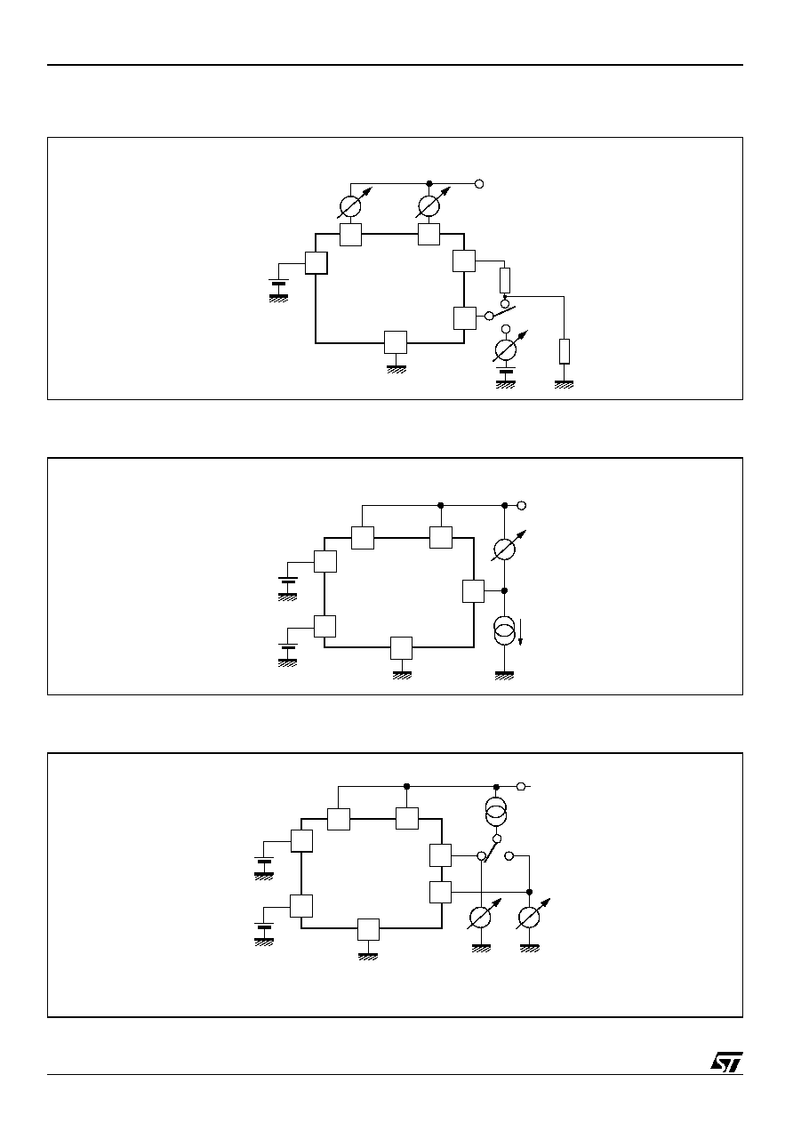
Figure 1: Measurement of I
1
, I
2
and I
6
Figure 2: Measurement of V
5H
Figure 3: Measurement of V
3L
and V
5L
1V
(a)
39k
5
1
(b)
I1
(a): I2 and I6 measurement
(b): I1 measurement
S
+Vs
2
6
I2
I6
4
7
2.2V
STV9302A
5.6k
- I5
5
1V
7
2.2V
1
4
+Vs
2
6
V
5H
STV9302A
+Vs
I3 or I5
3
5
V
5L
V
3L
(a)
(b)
(a): V
5L
measurement
(b): V
3L
measurement
STV9302A
1V
7
4
2
6
2.2V
1
5/15
STV9302A
Application Hints
4
Application Hints
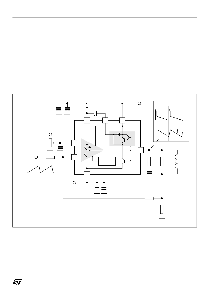
The yoke can be coupled either in AC or DC.
4.1
DC-coupled Application
When DC coupled (see
Figure 4
), the display vertical position can be adjusted with input bias. On
the other hand, 2 supply sources (V
S
and -V
EE
) are required.
A Stand-by state will be reached by switching OFF the positive supply alone. In this state, where
both inputs are the same voltage as pin 2 or higher, the output will sink negligible current from the
deviation coil.
4.1.1
Application Hints
For calculations, treat the IC as an op-amp, where the feedback loop maintains V
1
= V
7
.
Figure 4: DC-coupled Application
R3
+Vs
R2
R1
Rd(*)
Yoke
Ly
Vertical Position
Adjustment
-V
EE
Vref
(*) recommended:
Ly
50
µ
s
-------------
Rd
Ly
20
µ
s
-------------
<
<
0.1µF
0.1µF
C
F
(47 to 100µF)
Power
Amplifier
Flyback
Generator
Thermal
Safety
470µF
470µF
Output
Current
Output
Voltage
I
p
000000000000000000
00000000000000000
000000000000000000 000000000000000000
000000000000000000
000000000000000000
00000000000000000
00000000000000000
7
3
2
5
6
1
4
V
M
V
m
+
-
0
.
22
µF
1.5