 | –≠–ª–µ–∫—Ç—Ä–æ–Ω–Ω—ã–π –∫–æ–º–ø–æ–Ω–µ–Ω—Ç: STV9325 | –°–∫–∞—á–∞—Ç—å:  PDF PDF  ZIP ZIP |
DATASHEET
June 2004
Revision 1.5
Æ
STV9325
Vertical Deflection Booster
for 2.5-A
PP
TV/Monitor Applications with 70-V Flyback Generator
Main Features
Power Amplifier
Flyback Generator
Stand-by Control
Output Current up to 2.5 App
Thermal Protection
Description
The STV9325 is a vertical deflection booster
designed for TV and monitor applications.
This device, supplied with up to 35 V, provides up to
2.5 App output current to drive the vertical
deflection yoke.
The internal flyback generator delivers flyback
voltages up to 75 V.
In double-supply applications, a stand-by state will
be reached by stopping the (+) supply alone.
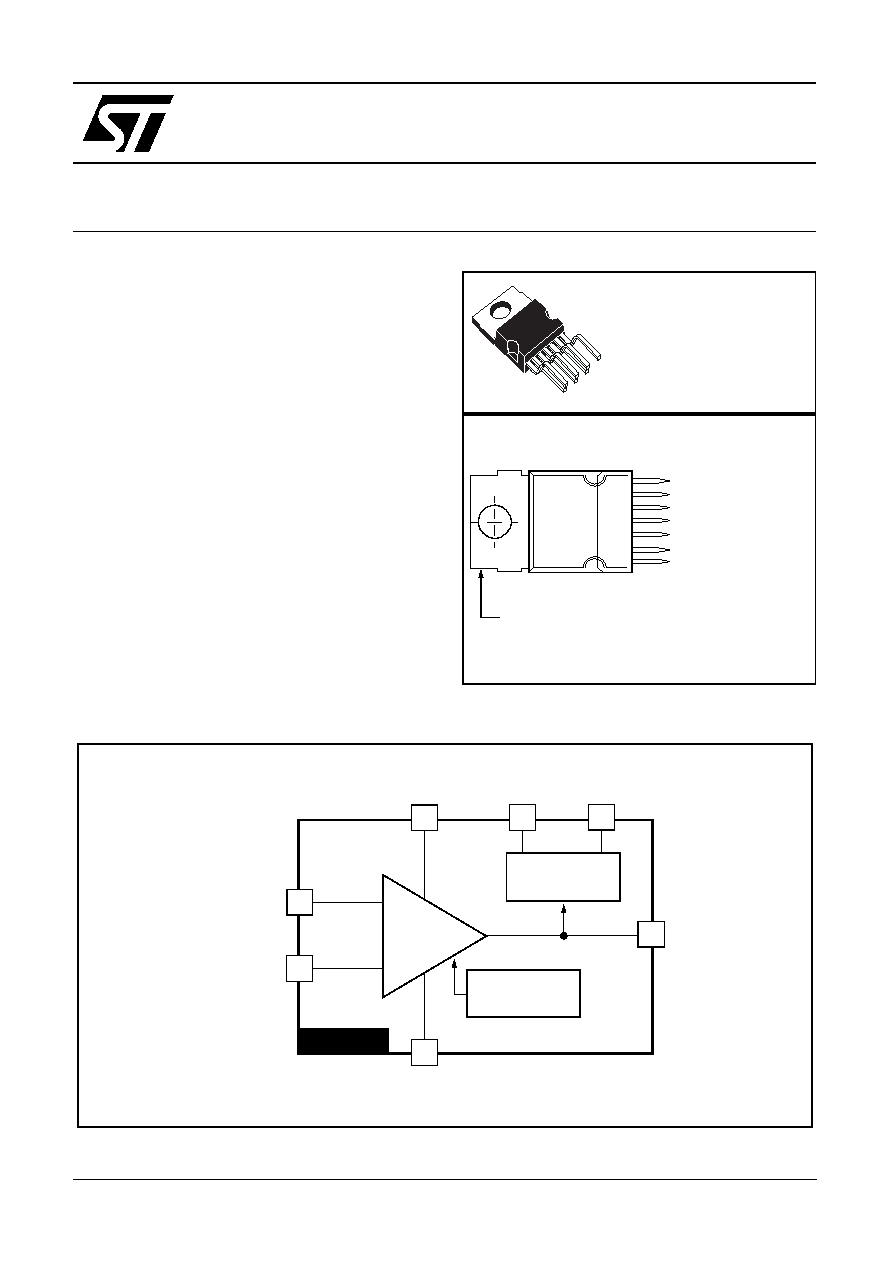
HEPTAWATT
(Plastic Package)
ORDER CODE: STV9325
7
6
5
4
3
2
1
Tab connected
Input (Non Inverting)
Output Stage Supply
Output
Ground Or Negative Supply
Flyback Generator
Supply Voltage
Input (Inverting)
to pin 4
1
Thermal
Protection
6
4
3
5
STV9325
+
-
Power
Amplifier
7
2
Flyback
Generator
Inverting
Non-Inverting
Input
Input
Ground or Negative Supply
Output
Flyback
Generator
Output Stage
Supply
Voltage
Supply
Absolute Maximum Ratings
STV9325
2/14
1
Absolute Maximum Ratings
Note:1. Usually the flyback voltage is slightly more than 2 x V
S
. This must be taken into consideration when
setting
V
S.
2. Versus pin 4
3. V3 is higher than V
S
during the first half of the flyback pulse.
4. Such repetitive output peak currents are usually observed just before and after the flyback pulse.
5. This non-repetitive output peak current can be observed, for example, during the Switch-On/Switch-
Off phases. This peak current is acceptable providing the SOA is respected (
Figure 8
and
Figure 9
).
6. All pins have a reverse diode towards pin 4, these diodes should never be forward-biased.
7. Input voltages must not exceed the lower value of either V
S
+ 2 or 40 volts.
2
Thermal Data
Symbol
Parameter
Value
Unit
Voltage
V
S
Supply Voltage (pin 2) -
Note 1
and
Note 2
40
V
V
5
, V
6
Flyback Peak Voltage -
Note 2
75
V
V
3
Voltage at Pin 3 -
Note 2
,
Note 3
and
Note 6
-0.4 to (V
S
+ 3)
V
V
1
, V
7
Amplifier Input Voltage -
Note 2
,
Note 6
and
Note 7
- 0.4 to (V
S
+ 2) or +40
V
Current
I
0
(1)
Output Peak Current at f = 50 to 200 Hz, t
10µs -
Note 4
±5
A
I
0
(2)
Output Peak Current non-repetitive -
Note 5
±2
A
I
3
Sink
Sink Current, t<1ms -
Note 3
2
A
I
3
Source
Source Current, t
<
1ms
2
A
I
3
Flyback pulse current at f=50 to 200 Hz, t
10
µ
s -
Note 4
±5
A
ESD Susceptibility
ESD1
Human body model (100 pF discharged through 1.5 k
)
2
kV
ESD2
EIAJ Standard (200 pF discharged through 0
)
300
V
Temperature
T
s
Storage Temperature
-40 to 150
∞C
T
j
Junction Temperature
+150
∞C
Symbol
Parameter
Value
Unit
R
thJC
Junction-to-Case Thermal Resistance
3
∞C/W
T
T
Temperature for Thermal Shutdown
150
∞C
T
J
Recommended Max. Junction Temperature
120
∞C

3/14
STV9325
Electrical Characteristics
3
Electrical Characteristics
(V
S
= 34 V, T
AMB
= 25∞C, unless otherwise specified)
8. In normal applications, the peak flyback voltage is slightly greater than 2 x (V
S
- V
4
). Therefore, (V
S
- V
4
) = 35 V is not allowed without special circuitry.
9. Refer to
Figure 4
, Stand-by condition.
Symbol
Parameter
Test Conditions
Min.
Typ.
Max.
Unit
Fig.
Supply
V
S
Operating Supply Voltage Range (V
2
-V
4
)
Note 8
10
35
V
I
2
Pin 2 Quiescent Current
I
3
= 0, I
5
= 0
5
20
mA
1
I
6
Pin 6 Quiescent Current
I
3
= 0, I
5
= 0, V
6
=35v
8
19
50
mA
1
Input
I
1
Input Bias Current
V
1
= 1 V, V
7
= 2.2 V
- 0.6
-1.5
µ
A
1
I
7
Input Bias Current
V
1
= 2.2 V, V
7
= 1 V
- 0.6
-1.5
µ
A
V
IR
Operating Input Voltage Range
0
V
S
- 2
V
V
I0
Offset Voltage
2
mV
V
I0
/dt
Offset Drift versus Temperature
10
µ
V/∞C
Output
I
0
Operating Peak Output Current
0
o
<Tcase<125
o
C
±1.25
A
V
5L
Output Saturation Voltage to pin 4
I
5
= 1.25 A
0.9
1.6
V
3
V
5H
Output Saturation Voltage to pin 6
I
5
= -1.25 A
1.5
2.2
V
2
Stand-by
V
5STBY
Output Voltage in Stand-by
V
1
= V
7
= V
S
= 0
See
Note 9
V
S
- 2
V
Miscellaneous
G
Voltage Gain
80
dB
V
D5-6
Diode Forward Voltage Between pins 5-6
I
5
= 1.25 A
1.5
2.1
V
V
D3-2
Diode Forward Voltage between pins 3-2
I
3
= 1.25 A
1.5
2.1
V
V
3SL
Saturation Voltage on pin 3
I
3
= 20 mA
0.4
1
V
3
V
3SH
Saturation Voltage to pin 2 (2nd part of flyback)
I
3
= -1.25 A
1.8
2.6
V

Electrical Characteristics
STV9325
4/14
Figure 1: Measurement of I
1
, I
2
and I
6
Figure 2: Measurement of V
5H
Figure 3: Measurement of V
3L
and V
5L
1V
(a)
39k
5
1
(b)
I1
(a): I2 and I6 measurement
(b): I1 measurement
S
+Vs
2
6
I2
I6
4
7
2.2V
STV9325
5.6k
- I5
5
1V
7
2.2V
1
4
+Vs
2
6
V
5H
STV9325
+Vs
I3 or I5
3
5
V
5L
V
3L
(a)
(b)
(a): V
5L
measurement
(b): V
3L
measurement
STV9325
1V
7
4
2
6
2.2V
1

5/14
STV9325
Application Hints
4
Application Hints
The yoke can be coupled either in AC or DC.
4.1
DC-coupled Application
When DC coupled (see
Figure 4
), the display vertical position can be adjusted with input bias. On
the other hand, 2 supply sources (V
S
and -V
EE
) are required.
A Stand-by state will be reached by switching OFF the positive supply alone. In this state, where
both inputs are the same voltage as pin 2 or higher, the output will sink negligible current from the
deviation coil.
4.1.1
Application Hints
For calculations, treat the IC as an op-amp, where the feedback loop maintains V
1
= V
7
.
Figure 4: DC-coupled Application
R3
+Vs
R2
R1
Rd(*)
Yoke
Ly
Vertical Position
Adjustment
-V
EE
Vref
(*) recommended:
Ly
50
µ
s
-------------
Rd
Ly
20
µ
s
-------------
<
<
0.1µF
0.1µF
C
F
(47 to 100µF)
Power
Amplifier
Flyback
Generator
Thermal
Safety
470µF
470µF
Output
Current
Output
Voltage
I
p
000000000
000000000
000000000
000000000
00000000
00000000
000000000
000000000
000000000
000000000
7
3
2
5
6
1
4
V
M
V
m
+
-
0.22µ
F
1.5