May 2000
1/7
This is preliminary information on a new product now in development. Details are subject to change without notice.
Version 1.1
STV9380
CLASS-D VERTICAL DEFLECTION AMPLIFIER FOR TV AND
MONITOR APPLICATION
TARGET SPECIFICATION
FEATURES
s
High Efficiency Power Amplifier
s
No Heatsink
s
Split Supply
s
Flyback Generator
s
Output Current up to 2.5 APP
s
Flyback Voltage up to 65V
s
Suitable for DC Coupling Application
DESCRIPTION
Designed for monitors and TVs, the STV9380 is a
class-D vertical deflection booster assembled in
PDIP20 Package.
It operates with supplies up to +/- 16V, provides
up to 2.5 App output current to drive the yoke. Fly-
back voltage is close to 65V.
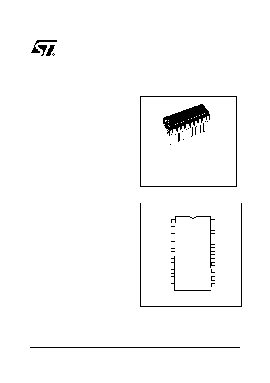
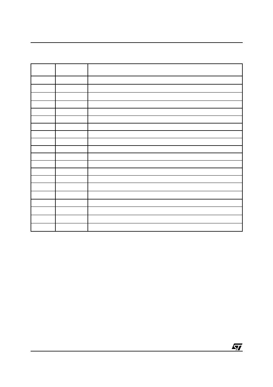
PIN CONNECTION
PDIP20
(14+3+3)
ORDER CODE:
STV9380
20
19
18
17
16
15
14
13
12
11
1
2
3
4
5
6
7
8
9
10
-V
CC
-V
CC
-V
CC
-V
CC
-V
CC
-V
CC
-V
CC
POW
+ V
CC
POW
+V
CC
EAout
IN+
IN-
SGND
OUT
CFLY +
CFLY -
BOOT
VREG
FEEDCAP
FREQ
1
STV9380
2/7
1 - PIN FUNCTIONS
Pin
Number
Name
Function
1
-V
CC
Negative supply
2
-V
CC
Negative supply
3
-V
CC
Negative supply
4
OUT
PWM Output
5
CFLY+
Flyback capacitor
6
CFLY-
Flyback capacitor
7
BOOT
Bootstrap capacitor
8
VREG
Internal voltage regulator
9
FEEDCAP
Feed-back integrated capacitor
10
FREQ
Frequency setting resistor
11
SGND
Signal Ground
12
IN-
Error amplifier inverting input
13
IN+
Error amplifier non-inverting input
14
EA out
Error amplifier output
15
+V
CC
Positive supply
16
+V
CC
POW
Positive Power supply
17
-VccPOW
Negative Power supply
18
-V
CC
Negative supply
19
-V
CC
Negative supply
20
-V
CC
Negative supply
2
ST
V9380
3/
7
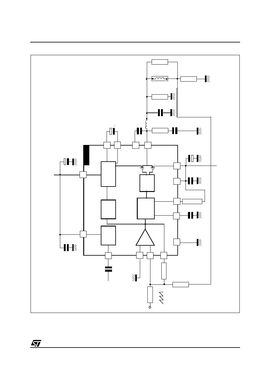
Fi
gu
re
1
.
Te
s
t
a
n
d A
p
p
l
i
c
a
t
i
o
n C
i
rc
ui
t
Flyback
Flyback
Output
Modulator
+
_
drive
generator
detection
+VCC
+VCC power
CFLYBACK
CFLY+
100nF
VREG
IN+
IN -
1k
10k
EA out
-VCC power
-VCC
-VCC
BOOT
Cboot
470nF
10k
4.7nF
FREQ
FEEDCAP
SGND
Pins 1,2,3,18,19,20
OUT
0.5
Deflect.
Yoke
CFLY-
+VCC
1mH
Input signal
1k
100nF
-VCC
100nF
100nF
470
�
F
470
�
F
STV9380
100
�
F
14
11
9
17
560pF
150
200
15
16
TDA9380
5
6
7
4
13
12
150
10
Vref
8
2
STV9380
4/7
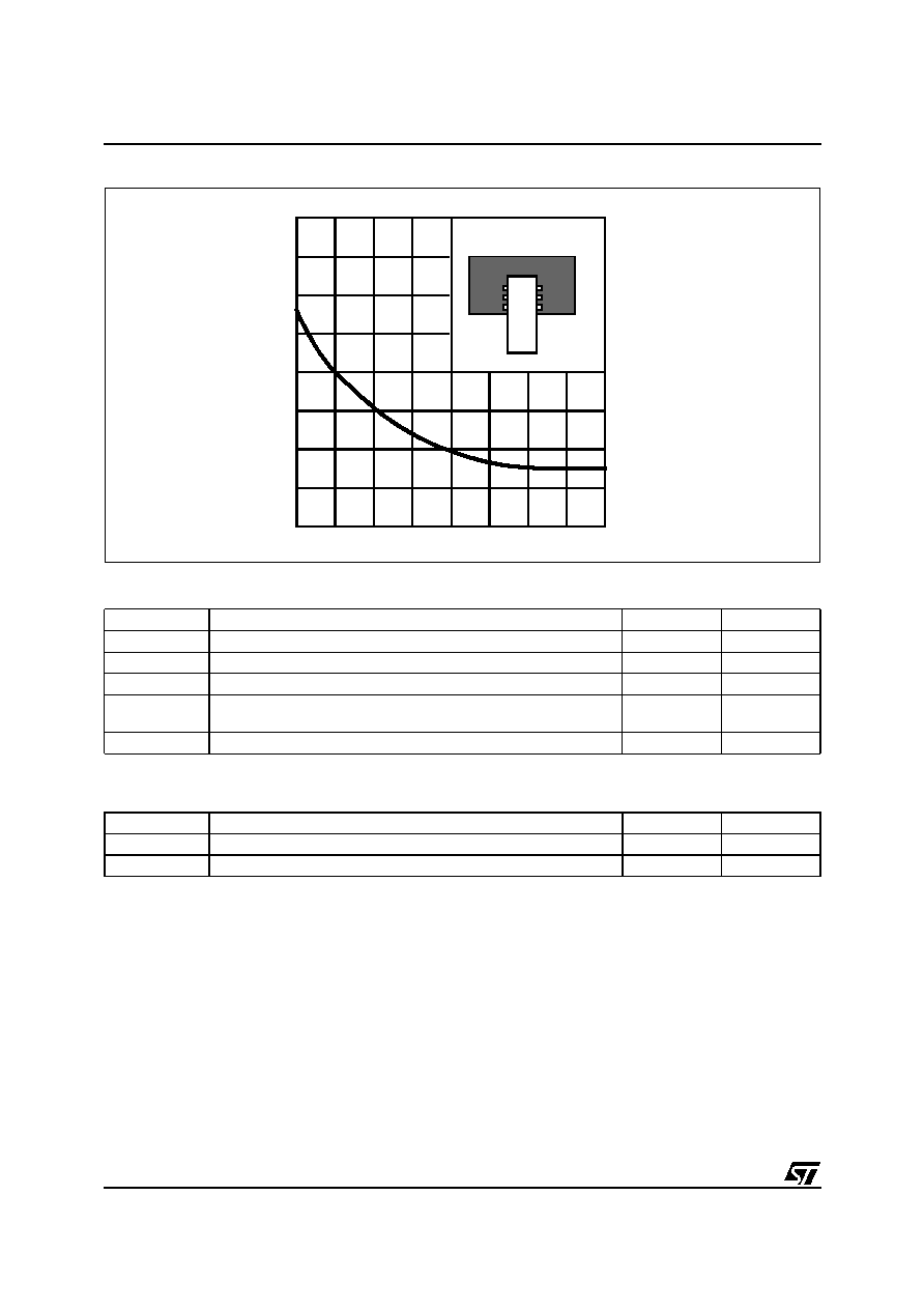
Figure 2. Rth with "on board" Square Heatsink vs. copper area
2 - ABSOLUTE MAXIMUM RATING
3 - THERMAL DATA
Symbol
Parameter
Value
Unit
VCC
DC Supply Voltage
�18
V
T
stg
, T
j
Storage and Junction Temperature
-40 to +150
�C
T
op
Operating Temperature Range
0 to +70
�C
VESD
ESD Susceptibility - Human Body Model (100 pF discharge through
1.5 k
)
�2
kV
Iout
Output current
�1.6
A
Symbol
Parameter
Value
Unit
R
th j-amb
Thermal resistance Junction to ambiant
80
�C/W
R
th j-pin
Thermal Resistance Junction to Pin
12
�C/W
0
4
8
12
Area(cm
2
)
30
40
50
60
R
thj-a
(�C/W)
D97AU675
COPPER AREA 35
THICKNESS
PC BOARD
2
STV9380
5/7
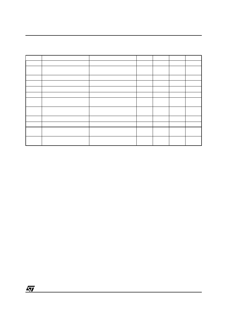
4 - ELECTRICAL CHARACTERISTICS
(refer to Figure 1 on page 3)
Tamb = 25�C unless otherwise specified, Vcc = �12V
Symbol
Parameter
Test Conditions
Min.
Typ.
Max.
Units
Vcc
Supply range
�10
�16
V
Iout
Maximum recommended out-
put current
�1.25
A
Iq
Quiescent supply current
Input voltage = 0
TBD
TBD
mA
I
13
, I
12
Amplifier Input bias current
-0.1
�
A
V
OS
Output Offset voltage
Input voltage = 0
-50
+50
mV
SVR
Supply voltage rejection
TBD
TBD
dB
Fly
thr
Flyback detection threshold
positive slope
V(14)
1.5
V
Fly
thf
Flyback detection threshold
negative slope
V(14)
0.5
V
Efficiency = P
o
/(P
o
+ P
d
)
P
o
= 3 W
TBD
Fsw
Switching frequency
120
140
160
kHz
Fsw - op
Switching frequency opera-
tive range
100
200
kHz
R
freq
Frequency controller resistor
range
7
10
14
k
2