 | –≠–ª–µ–∫—Ç—Ä–æ–Ω–Ω—ã–π –∫–æ–º–ø–æ–Ω–µ–Ω—Ç: STV9380A | –°–∫–∞—á–∞—Ç—å:  PDF PDF  ZIP ZIP |
This is preliminary information on a new product now in development or undergoing evaluation. Details are subject to change without notice.
October 2003
1/10
Æ
STV9380A
Class-D Vertical Deflection Amplifier
for 2.5 Amp TV and Monitor Applications
Main Features
s
High-Efficiency Power Amplifier
s
No Heatsink
s
Split Supply
s
Internal Flyback Generator
s
Output Current up to 2.5 A
PP
s
Suitable for DC Coupling Applications
s
Few External Components
s
Protection against Low V
CC
Description
Designed for TV and monitor applications, the
STV9380A is a Class-D vertical deflection booster
assembled in a 20-pin plastic DIP package.
It operates with supplies up to ±18 V and provides
an output current up to 2.5 A
PP
to drive the yoke.
The internal flyback generator avoids the need for
an extra power supply.
PDIP 20
Order Code: STV9380A
-V
CC
-V
CC
-V
CC
-V
CC
-V
CC
-V
CC
-V
CC
POW
+ V
CC
POW
+V
CC
EAout
IN+
IN-
SGND
OUT
CFLY +
CFLY -
BOOT
VREG
FEEDCAP
FREQ
1
2
3
4
5
6
7
8
9
10
20
19
18
17
16
15
14
13
12
11
7
Pin Functions
STV9380A
2/10
1
Pin Functions
Note 1. The voltage reference, accessible on pin 8, is for internal use only. No additional components
should be connected to this pin except the decoupling capacitor.
2
Functional Description
The STV9380A is a vertical deflection circuit operating in Class D. Class D is a modulation method
where the output transistors work in switching mode at high frequency. The output signal is restored
by filtering the output square wave with an external LC filter. The major interest of this IC is the
comparatively low power dissipation in regards to traditional amplifiers operating in class AB,
eliminating the need of an heatsink.
Except for the output stage which uses Class D modulation, the circuit operation is similar to
the
one of a traditional linear vertical amplifier.
A (sawtooth) reference signal has to be applied to the circuit which can accept a differential or
single ended signal. This sawtooth is amplified and applied as a current to the deflection yoke. This
current is measured by means of a low value resistor. The resulting voltage is used as a feedback
signal to guarantee the conformity of the yoke current with the reference input signal.
The overvoltage necessary for a fast retrace is obtained with a chemical capacitor charged
at the
power supply voltage of the circuit. At the flyback moment, this capacitor is connected in series with
the output stage power supply. This method, used for several years with the linear vertical boosters
and called "internal flyback" or "flyback generator", avoids the need of an additional power supply,
while reducing the flyback duration.
The circuit uses a BCD process that combines Bipolar, CMOS and DMOS devices. The output
stage is composed of low-R
ON
N-channel DMOS transistors.
Table 1: STV9380A Pin Descriptions
Pin
Name
Function
Pin
Name
Function
1
-V
CC
Negative Supply
11
SGND
Signal Ground
2
-V
CC
Negative Supply
12
IN-
Error Amplifier Inverting Input
3
-V
CC
Negative Supply
13
IN+
Error Amplifier Non-inverting Input
4
OUT
PWM Output
14
EA out
Error Amplifier Output
5
CFLY+
Flyback Capacitor
15
+V
CC
Positive Supply
6
CFLY-
Flyback Capacitor
16
+V
CC
POW
Positive Power Supply
7
BOOT
Bootstrap Capacitor
17
-VccPOW
Negative Power Supply
8
VREG
Internal Voltage Regulator
18
-V
CC
Negative Supply
9
FEEDCAP
Feed-back Integrating Capacitor
19
-V
CC
Negative Supply
10
FREQ
Frequency Setting Resistor
20
-V
CC
Negative Supply
3/
1
0
S
T
V
9380
A
F
u
n
ct
ion
a
l D
e
s
c
r
i
p
t
io
n
F
i
g
u
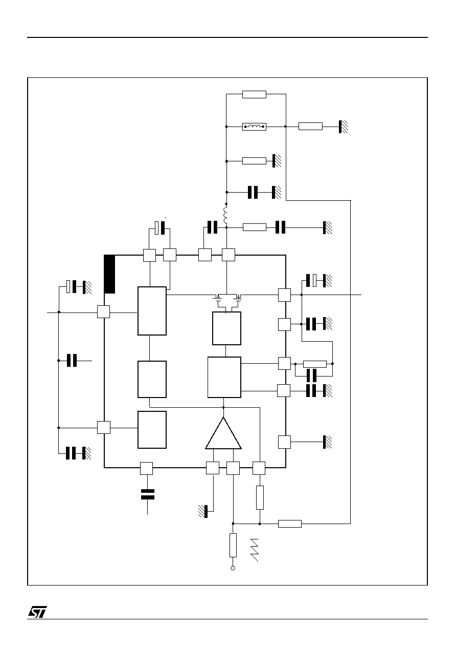
re 1: T
est an
d
Ap
p
l
i
c
ati
o
n
Ci
rc
u
i
t
Di
ag
r
a
m
Flyback
Flyback
Output
Modulator
+
_
Drive
Generator
Detection
+VCC
+VCC power
CFLYBACK
CFLY+
100nF
VREG
IN+
IN -
1 k
10k
EA out
-VCC power
-VCC
-VCC
BOOT
Cboot
470nF
10k
4.7nF
FREQ
FEEDCAP
SGND
Pins 1, 2, 3, 18, 19 and 20
OUT
0.5
Deflect.
Yoke*
CFLY-
+VCC
1mH
Input Signal
1k
220nF
-VCC
100nF
100nF
1000
µ
F
1000
µ
F
STV9380A
100
µ
F
14
11
9
17
560pF
150
200
15
16
8
STV9380A
5
6
7
4
13
12
150
10
V
REF
-VCC
470pF
* Deflection yoke characteristics: R = 5.5
, L = 7mH
100nF
Sense
Resistor
f
VERT
= 50 Hz
Absolute Maximum Ratings
STV9380A
4/10
3
Absolute Maximum Ratings
Note 1. During the flyback with V
CC
= ±18 V, the maximum output voltage (pin 4) is close to 72 V, with
respect to -V
CC
(pins 1, 2, 3, 18, 19 and 20).
4
Thermal Data
Pins 1, 2, 3, 18, 19 and 20 are internally connected together and participate in heat evacuation.
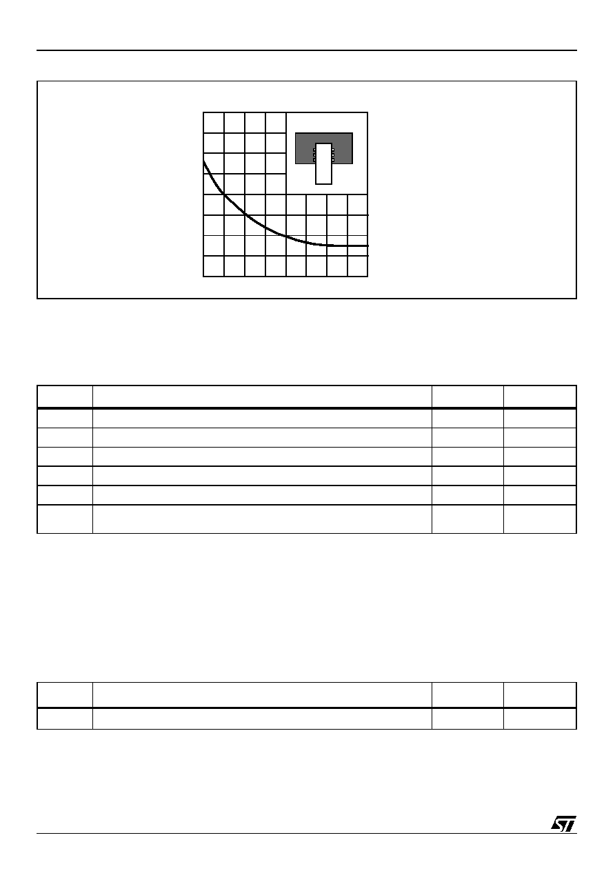
Figure 2: Thermal Resistance with "On-board" Square Heatsink vs. Copper Area
Symbol
Parameter
Value
Unit
V
CC
DC Supply Voltage
±20
V
T
STG
, T
J
Storage and Junction Temperature
-40 to +150
∞C
T
OP
Operating Temperature Range
-20 to +70
∞C
V
ESD
ESD Susceptibility - Human Body Model (100 pF discharge through 1.5 k
)
±2
kV
I
OUT
Output current
±1.6
A
V
OUT
Maximum output voltage (pin 4) with respect to -Vcc
(pins 1, 2, 3, 18, 19 and 20) and during flyback (see
Note 1
)
80
V
Symbol
Parameter
Value
Unit
R
thJA
Junction-to-Ambient Thermal Resistance
70
∞C/W
0
4
8
12
Area (cm≤)
40
50
60
70
R
thJA
(∞C/W)
Copper Area 35 µm
Thickness
PC Board
5/10
STV9380A
Electrical Characteristics
5
Electrical Characteristics
T
AMB
= 25∞ C, V
CC
= ±12 V and f
VERT
= 50 Hz unless otherwise specified (refer to
Figure 1
)
Note 1. Input voltage = 0, measured after the filter (e.g. across the 470 nF filter capacitor)
2. Supply rejection of the positive or negative power supply. V
CC
ripple
=1 V
PP
, f =100 Hz, measured
on the sense resistor.
3. Power dissipated in the circuit in the case of the application from
Figure 1
and the current in the
deflection yoke adjusted to 2.5 A
PP
. The corresponding power dissipated in the vertical deflection
yoke is 2.8 W.
Symbol
Parameter
Test Conditions
Min.
Typ.
Max.
Units
+V
CC
Positive Supply Range
+10
+18
V
-V
CC
Negative Supply Range
-18
-10
V
V
CC
Maximum recommended difference
between +V
CC
and |-V
CC
|
±4
V
V
CCSTART
Low V
CC
Detection
±6.5
V
I
Q
Quiescent Supply Current
Input Voltage = 0
14
mA
I
Y
Maximum Vertical Yoke Current
±1.25
A
I
13
, I
12
Amplifier Input Bias Current
-0.1
µ
A
V
OS
Output Offset Voltage
Note 1
-50
+50
mV
SVR
Supply Voltage Rejection
Note 2
82
dB
Fly
THR
Flyback Detection Threshold
(Positive Slope)
V(14)
1.5
V
Fly
THF
Flyback Detection Threshold
(Negative Slope)
V(14)
0.5
V
P
D
Integrated Circuit
Dissipated Power
Note 3
1.1
W
f
SW
Switching Frequency
R
FREQ
= 10 k
120
140
160
kHz
f
SW-OP
Switching Frequency Operative Range
100
200
kHz
R
FREQ
Frequency Controller Resistor Range
Pin 10
7
10
14
k