 | –≠–ª–µ–∫—Ç—Ä–æ–Ω–Ω—ã–π –∫–æ–º–ø–æ–Ω–µ–Ω—Ç: STV9423 | –°–∫–∞—á–∞—Ç—å:  PDF PDF  ZIP ZIP |
STV9422
STV9424
MULTISYNC ON-SCREEN DISPLAY FOR MONITOR
October 1995
.
CMOS SINGLE CHIP OSD FOR MONITOR
.
BUILT IN 1 KBYTE RAM HOLDING :
- PAGES' DESCRIPTORS
- CHARACTER CODES
- USER DEFINABLE CHARACTERS
.
128 ALPHANUMERIC CHARACTERS OR
GRAPHIC
SYMBOLS
IN INTERNAL ROM
(12 x 18 DOT MATRIX)
.
UP TO 26 USER DEFINABLE CHARACTERS
.
INTERNAL HORIZONTAL PLL (15 TO 120kHz)
.
PROGRAMMABLE VERTICAL HEIGHT OF
CHARACTER WITH A SLICE INTERPOLATOR
TO MEET MULTI-SYNCH REQUIREMENTS
.
PROGRAMMABLE VERTICAL AND HORI-
ZONTAL POSITIONING
.
FLEXIBLE SCREEN DESCRIPTION
.
CHARACTER BY CHARACTER COLOR SE-
LECTION (UP TO 8 DIFFERENT COLORS)
.
PROGRAMMABLE BACKGROUND (COLOR,
TRANSPARENT OR WITH SHADOWING)
.
CHARACTER BLINKING
.
2-WIRES ASYNCHRONOUS SERIAL MCU
INTERFACE (I
2
C PROTOCOL)
.
8 x 8 BITS PWM DAC OUTPUTS
.
SINGLE POSITIVE 5V SUPPLY
SHRINK 24
(Plastic Package)
ORDER CODE : STV9422
DESCRIPTION
The STV9422/24 is an ON SCREEN DISPLAY for
monitor. It is built as a slave peripheral connected
to a host MCU via a serial I
2
C bus. It includes a
display memory, controls all the display attributes
and generates pixels from the data read in its on
chip memory. The line PLL and a special slice
interpolator allow to have a display aspect which
does not depend on the line and frame frequencies.
I
2
C interface allows MCU to make transparent in-
ternal access to prepare the next pages during the
display of the current page. Toggle from one page
to another by programming only one register.
8 x 8 bits PWM DAC are available to provide DC
voltage control to other peripherals.
The STV9422/24 provides the user an easy to use
and cost effective solution to display alphanumeric
or graphic information on monitor screen.
DIP16
(Plastic Package)
ORDER CODE : STV9424
1/15
PIN DESCRIPTION
Symbol
Pin Number
I/O
Description
SDIP24
DIP16
PWM0
1
-
O
DAC0 Output
PWM1
2
-
O
DAC1 Output
FBLK
3
1
O
Fast Blanking Output
V-SYNC
4
2
I
Vertical Sync Input
H-SYNC
5
3
I
Horizontal Sync Input
V
DD
6
4
S
+5V Supply
PXCK
7
5
O
Pixel Frequency Output
CKOUT
8
6
O
Clock Output
XTAL OUT
9
7
O
Crystal Output
XTAL IN
10
8
I
Crystal or Clock Input
PWM2
11
-
O
DAC2 Output
PWM3
12
-
O
DAC3 Output
PWM4
13
-
O
DAC4 Output
PWM5
14
-
O
DAC5 Output
SCL
15
9
I
Serial Clock
SDA
16
10
I/O
Serial Input/output Data
RESET
17
11
I
Reset Input (Active Low)
GND
18
12
S
Ground
R
19
13
O
Red Output
G
20
14
O
Green Output
B
21
15
O
Blue Output
TEST
22
16
I
Reserved (grounded in Normal Operation)
PWM6
23
-
O
DAC6 Output
PWM7
24
-
O
DAC7 Output
9422-01.TBL
9422-01.EPS
/
9424-01.EPS
PIN CONNECTIONS
1
2
3
4
5
6
7
8
9
10
20
19
18
17
16
15
14
13
24
23
22
21
11
12
PWM7
PWM6
PWM5
PWM4
PWM3
PWM2
PWM1
PWM0
SDA
SCL
GND
FBLK
B
G
R
RESET
VSYNC
HSYNC
CKOUT
XTAL IN
XTAL OUT
TEST
V
DD
PXCK
SDIP24 (STV9422)
1
2
3
4
5
6
7
8
16
15
14
13
12
11
10
9
FBLK
V-SYNC
H-SYNC
PXCK
CKOUT
XTAL OUT
XTAL IN
V
DD
TEST
B
G
R
GND
RESET
SDA
SCL
DIP16 (STV9424)
STV9422 - STV9424
2/15
P WM3
P WM2
P WM1
P WM0
12
11
2
1
P WM7
P WM6
P WM5
P WM4
24
23
14
13
CKOUT
HS YNC
VSYNC
RE S ET
R
G
B
FBLK
GND
S CL
S DA
XTAL
IN
XTAL
OUT
P XCK
TES T
Addres s /Data
HORIZONTAL
DIGITAL P LL
4K ROM
(128 cha racte rs )
1K RAM
P a ge Des criptors +
Us er Define d Cha r.
DISP LAY
CONTROLLER
I C BUS
INTERFACE
2
8
5
4
17
19
20
21
3
18
15
16
S TV9422
V
DD
10
9
7
6
22
PWM
9422-02.EPS
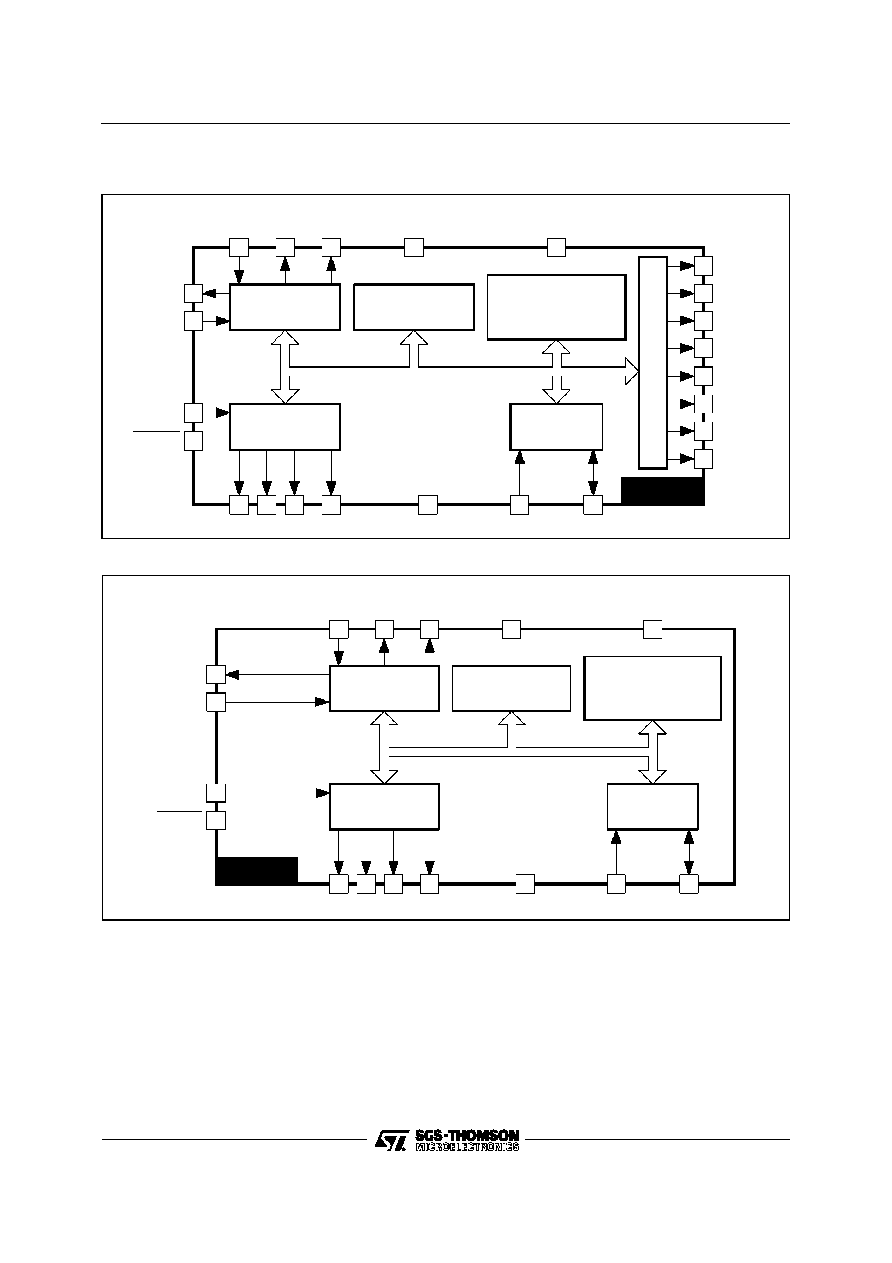
BLOCK DIAGRAMS
STV9422
1
2
3
4
5
6
7
8
9
10
11
12
13
14
15
16
CKOUT
HSYNC
VSYNC
RES ET
R
G
B
FBLK
GND
S CL
S DA
XTAL
IN
XTAL
OUT
PXCK
TEST
V
DD
Addre s s /Data
HORIZONTAL
DIGITAL P LL
4K ROM
(128 ch a racte rs)
1 K RAM
Pa ge De s criptors +
Us e r De fine d Cha r.
DISPLAY
CONTROLLER
I C BUS
INTERFACE
2
S TV9424
9424-02.EPS
STV9424
STV9422 - STV9424
3/15
ABSOLUTE MAXIMUM RATINGS
Symbol
Parameter
Value
Unit
V
DD
Supply Voltage
-0.3, +7.0
V
V
IN
Input Voltage
-0.3, +7.0
V
T
oper
Operating Ambient Temperature
0, +70
∞
C
T
stg
Storage Temperature
-40, +125
∞
C
9422-02.TBL
ELECTRICAL CHARACTERISTICS
(V
DD
= 5V, V
SS
= 0V, T
A
= 0 to 70
∞
C, F
XTAL
= 8 to 15MHz, TEST = 0 V, unless otherwise specified)
Symbol
Parameter
Min.
Typ.
Max.
Unit
SUPPLY
V
DD
Supply Voltage
4.75
5
5.25
V
I
DD
Supply Current
-
-
50
mA
INPUTS
SCL, SDA, TEST, RESET, V-SYNC and H-SYNC
V
IL
Input Low Voltage
0.8
V
V
IH
Input High Voltage
0.8V
DD
V
I
IL
Input Leakage Current
-20
+20
µ
A
OUTPUTS
R, G, B, FBLK, SDA, CKOUT, PXCK and PWMi (i = 0 to 7)
V
OL
Output Low Voltage (I
OL
= 1.6mA)
0
0.4
V
V
OH
Output High Voltage (I
OL
= -0.1mA)
0.8V
DD
V
DD
V
9422-03.TBL
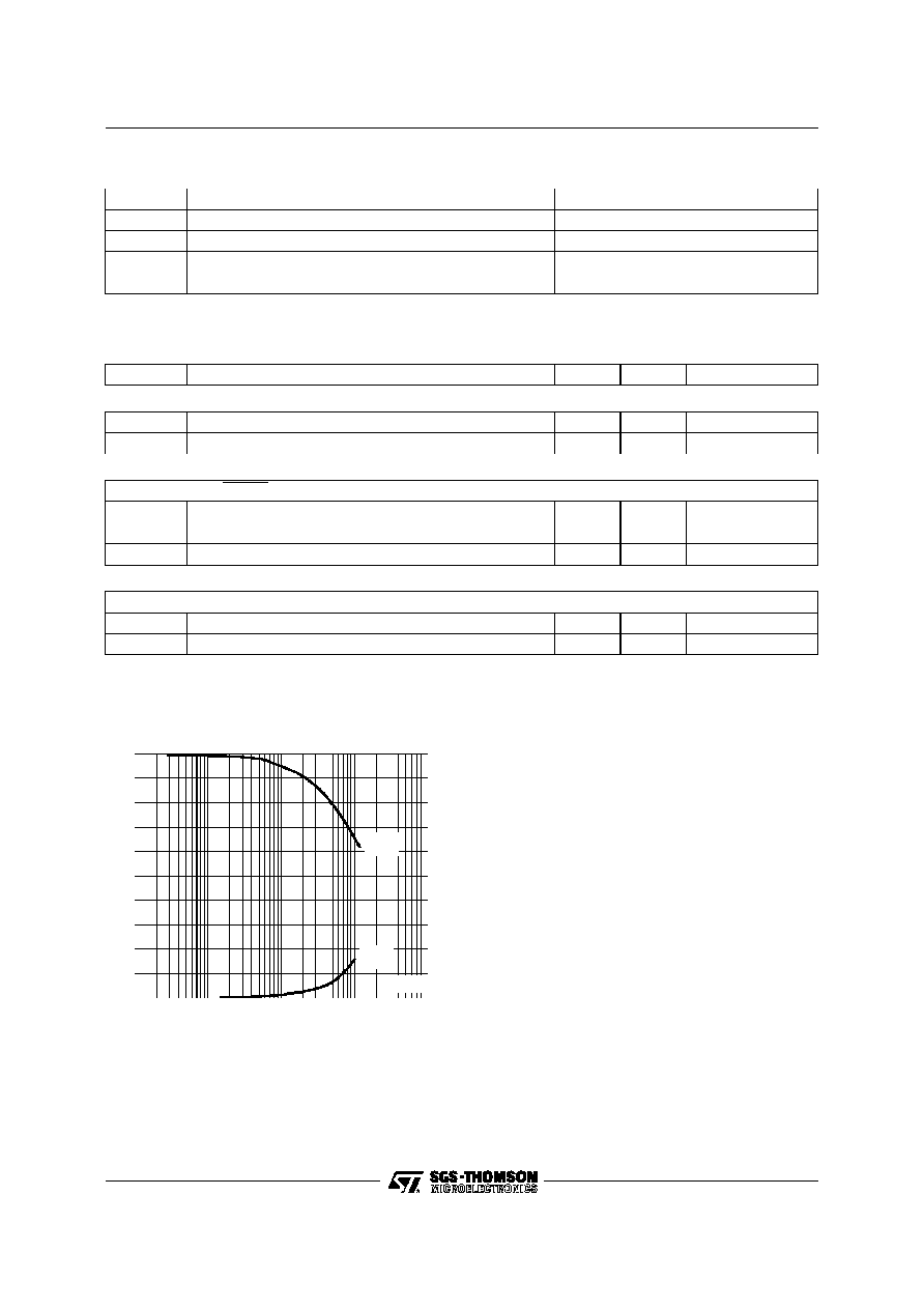
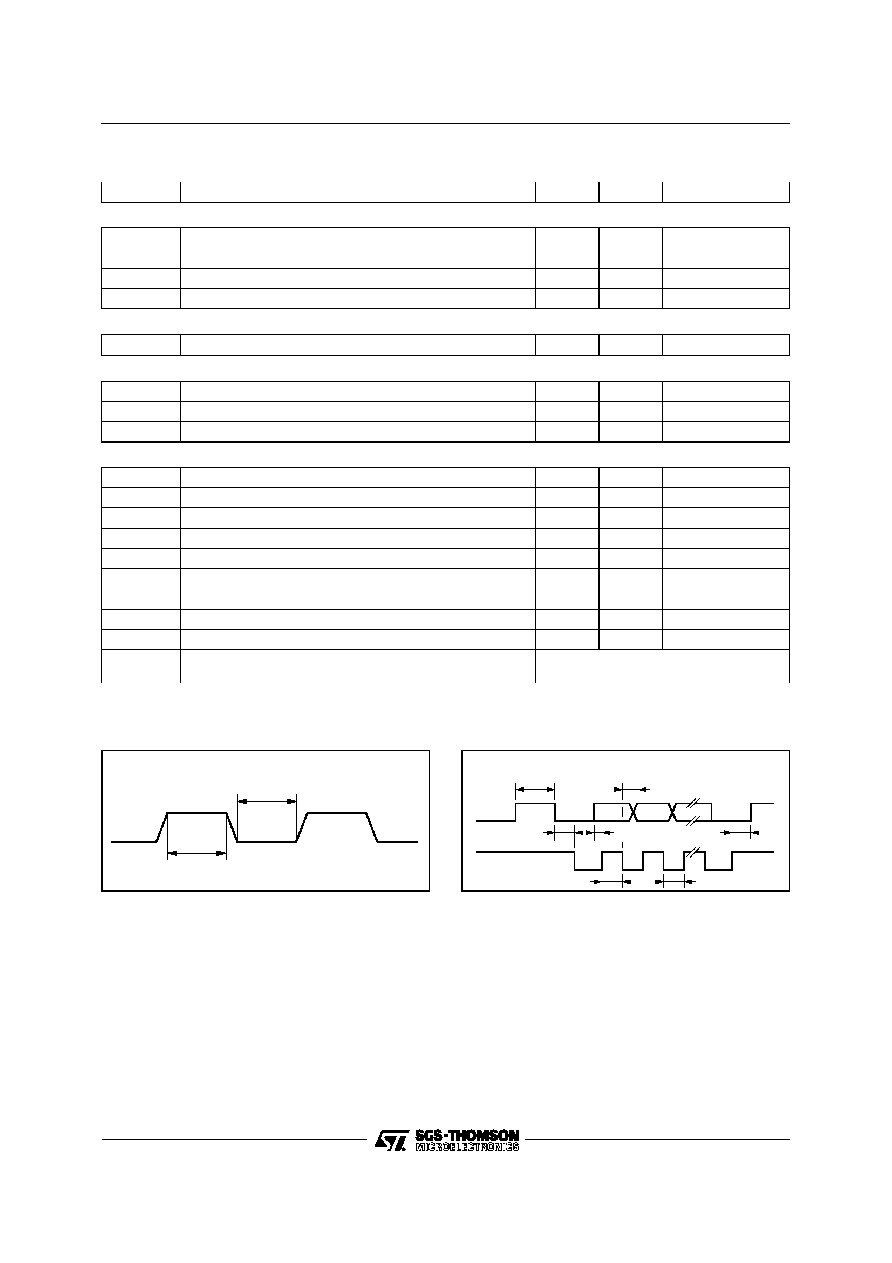
For R, G, B and FBLK outputs, see Figure 1.
5
2.5
0
10
-5
10
-4
10
-3
10
-2
10
-1
I (A)
(V)
,
V
OL
OH
V
V
OL
OH
V
9422-17.EPS
Figure 1 : Typical R, G, B Outputs Characteristics
STV9422 - STV9424
4/15
TIMINGS
Symbol
Parameter
Min.
Typ.
Max.
Unit
OSCILATOR INPUT : XTI (see Figure 2)
t
WH
Clock High Level
20
ns
t
WL
Clock Low Level
20
ns
f
XTAL
Clock Frequency
6
15
MHz
f
PXL
Pixel Frequency
40
MHz
RESET
t
RES
Reset Low Level Pulse
4
µ
s
R, G, B, FBLK (C
LOAD
= 30pF)
t
R
Rise Time (Note 1)
5
ns
t
F
Fall Time (Note 1)
5
ns
t
SKEW
Skew between R, G, B, FBLK (Note 1)
5
ns
I
2
C INTERFACE : SDA AND SCL (see Figure 3)
f
SCL
SCL Clock Frequency
0
1
MHz
t
BUF
Time the bus must be free between 2 access
500
ns
t
HDS
Hold Time for Start Condition
500
ns
t
SUP
Set up Time for Stop Condition
500
ns
t
LOW
The Low Period of Clock
400
ns
t
HIGH
The High Period of Clock
400
ns
t
HDAT
Hold Time Data
0
ns
t
SUDAT
Set up Time Data
375
ns
t
F
Fall Time of SDA
20
ns
t
R
Rise Time of Both SCL and SDA
Depend on the pull-up resistor
and the load capacitance
Note 1 : These parameters are not tested on each unit. They are measured during our internal qualification procedure which includes
characterization on batches comming from corners of our processes and also temperature characterization.
9422-04.TBL
XTI
t
W H
t
WL
9422-03.EPS
Figure 2
S DA
t
BUF
S CL
t
HDAT
S TOP
S TAR T
DATA
S TOP
t
SUDAT
t
HDS
t
SUP
t
HIGH
t
LOW
9422-04.EPS
Figure 3
STV9422 - STV9424
5/15
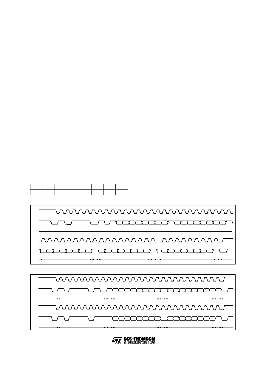
SCL
SDA
R/W
A7
A6
A5
A4
A3
A2
A1
A0
-
-
A13
A12
A11
A10
A9
A8
I
2
C Slave Address
ACK
LSB Address
ACK
MSB Address
ACK
Start
D7
D6
D5
D4
D3
D2
D1
D0
D7
D6
D5
D4
D3
D2
D1
D0
D7
D6
D5
D4
D3
D2
D1
D0
ACK
ACK
Data Byte 1
Data Byte 2
ACK
Data Byte n
Stop
SCL
SDA
9422-05.AI
Figure 3 : STV9422/I
2
C Write Operation
SCL
SDA
R/W
A7
A6
A5
A4
A3
A2
A1
A0
I
1
C Slave Address
ACK
LSB Address
ACK
MSB Address
ACK
Start
-
-
A13 A12 A10 A10 A9
A8
Stop
SCL
SDA
R/W
D7
D6
D5
D4
D3
D2
D1
D0
I
1
C Slave Address
ACK
ACK
Data Byte n
ACK
Start
D7
D6
D5
D4
D3
D2
D1
D0
Stop
Data Byte 1
9422-06.EPS
Figure 4 : STV9422/I
2
C Read Operation
FUNCTIONAL DESCRIPTION
The STV9422/24 display processor operation is
controlled by a host MCU via the I
2
C interface. It is
fully programmable through 16 internal read/write
registers (8 for STV9424) and performs all the
display functions by generating pixels from data
stored in its internal memory. After the page down-
loading from the MCU, the STV9422/24 refreshes
screen by its built in processor, without any MCU
control (access).In addition, the host MCU has a
direct access to the on chip 1Kbytes RAM during
the display of the current page to make any update
of its contents.
With the STV9422/24, a page displayed on the
screen is made of several strips which can be of 2
types : spacing or character and which are de-
scribed by a table of descriptors and character
codes in RAM. Several pages can be downloaded
at the same time in the RAM and the choice of the
current display page is made by programming the
CONTROL register.
I - Serial Interface
The 2-wires serial interface is an I
2
C interface. To
be connected to the I
2
C bus, a device must own its
sl ave ad dr ess ; the sla ve address of t he
STV9422/24 is BA (in hexadecimal).
A6
A5
A4
A3
A2
A1
A0
R/W
1
0
1
1
1
0
1
I.1 - Data Transfer in Write Mode
The host MCU can write data into the STV9422/24
registers or RAM.
To write data into the STV9422/24, after a start, the
MCU must send (Figure 3) :
- First, the I
2
C address slave byte with a low level
for the R/W bit,
- The two bytes of the internal address where the
MCU wants to write data(s),
- The successive bytes of data(s).
All bytes are sent MS bit first and the write data
transfer is closed by a stop.
I.2 - Data Transfer in Read Mode
The host MCU can read data from the STV9422/24
registers, RAM or ROM.
To read data from the STV9422/24 (Figure 4), the
MCU must send 2 different I
2
C sequences.
The first one is made of I
2
C slave address byte with
R/W bit at low level and the 2 internal address
bytes.
The second one is made of I
2
C slave address byte
with R/W bit at high level and all the successive
data bytes read at successive addresses starting
from the initial address given by the first sequence.
STV9422 - STV9424
6/15
FUNCTIONAL DESCRIPTION (continued)
I.3 - Addressing Space
STV9422/24registers, RAM and ROM are mapped
in a 16Kbytes addressing space. The mapping is
the following :
0000
1024 bytes RAM
Descriptors character
codes user definable
characters
03FF
0400
Empty Space
1FFF
2000
Character
Generator ROM
32FF
3300
Empty Space
3FFF
3FF0
Internal
Registers
3FFF
I.4 - Register Set
LINE DURATION
3FF0
VSP
HSP
LD5 LD4 LD3 LD2 LD1 LD0
*
0
0
1
1
1
1
1
1
VSP
: V-SYNC active edge selection
= 0 : falling egde, = 1 : rising edge
HSP
: H-SYNC active edge selection
= 0 : falling egde, = 1 : rising edge
LD[5:0] : LINE DURATION
(number of pixel period per line divided
by 12 ie. Unit = 12 pixel periods).
HORIZONTAL DELAY
3FF1 DD7 DD6 DD5 DD4 DD3 DD2 DD1 DD0
*
0
0
0
0
1
0
0
0
DD[7:0] : HORIZONTAL DISPLAY DELAY from
the H-SYNC reference falling edge to
the 1
st
pixel position of the character
strips. Unit = 3 pixel periods.
CHARACTERS HEIGHT
3FF2
-
-
CH5 CH4 CH3 CH2 CH1 CH0
*
-
-
0
1
0
0
1
0
CH[5:0] : HEIGHT of the character strips in scan
lines. For each scan line, the number of
the slice which is displayed is given by :
SLICE-NUMBER =
round
SCAN
±
LINE
±
NUMBER x 18
CH[5:0]
.
SCAN-LINE-NUMBER = Number of the
current scan line of the strip.
DISPLAY CONTROL
3FF3
OSD
FBK
FL1
FL0
-
P8
P7
P6
*
0
0
0
0
-
0
0
0
OSD
: ON/OFF (if 0, R, G, B and FBLK are 0).
FBK
: Fast blanking control :
= 1 : FBLK = 1, forcing black where these
is no display,
= 0 : FBLK is active only during character
display.
FL[1:0] : Flashing mode :
- 00 : No flashing. The character
attribute is ignored,
- 01 : 1/1 flashing (a duty cycle = 50%),
- 10 : 1/3 flashing,
- 11 : 3/1 flashing.
P[8:6]
: Address of the 1
st
descriptor of the
current displayed pages.
P[13:9] and P[5:0] = 0 ; up to 8 different
pages can be stored in the RAM.
LOCKING CONDITION TIME CONSTANT
3FF4
FR
AS2
AS1
AS0
-
BS2
BS1
BS0
*
0
0
1
0
-
0
1
0
FR
: Free Running ; if = 1 PLL is disabled and
the pixel frequency keeps its last value.
AS[2:0] : P h a s e c o ns t an t dur i n g l oc k in g
conditions.
BS[2:0] : Frequency constant during locking
conditions.
CAPTURE PROCESS TIME CONSTANT
3FF5
-
AF2
AF1
AF0
-
BF2
BF1
BF0
*
-
0
1
1
-
0
1
1
AF[2:0] : Phase constant during the capture
process.
BF[2:0] : Frequency constant during the capture
process.
INITIAL PIXEL PERIOD
3FF6 PP7
PP6
PP5
PP4
PP3 PP2
PP1 PP0
*
0
0
1
0
1
0
0
0
PP[7:0] : Value to initialize the pixel period of the
PLL.
FREQUENCY MULTIPLIER
3FF7
-
-
-
-
FM3 FM2 FM1 FM0
*
-
-
-
-
1
0
1
0
FM[3:0] : Frequency multiplier of the crystal
frequency to reach the high frequency
used by the PLL to derive the pixel
frequency.
STV9422 - STV9424
7/15
FUNCTIONAL DESCRIPTION (continued)
The last fourth registers described below are only
available with the STV9422 :
PULSE WIDTH MODULATOR 0 (STV9422)
3FF8
V07
V06
V05
V04
V03
V02
V01
V00
*
0
0
0
0
0
0
0
0
V0[7:0] : Digital value of the 1
st
PWM D to A
converter (Pin1).
PULSE WIDTH MODULATOR 1 (STV9422)
3FF9
V17
V16
V15
V14
V13
V12
V11
V10
*
0
0
0
0
0
0
0
0
V1[7:0] : Digital value of the 2
nd
PWM DAC (Pin2).
PULSE WIDTH MODULATOR 2 (STV9422)
3FFA
V27
V26
V25
V24
V23
V22
V21
V20
*
0
0
0
0
0
0
0
0
V2[7:0] : Digital value of the 3
rd
PWM DAC
(Pin11).
PULSE WIDTH MODULATOR 3 (STV9422)
3FFB
V37
V36
V35
V34
V33
V32
V31
V30
*
0
0
0
0
0
0
0
0
V3[7:0] : Digital value of the 4
th
PWM DAC
(Pin12).
PULSE WIDTH MODULATOR 4 (STV9422)
3FFC
V47
V46
V45
V44
V43
V42
V41
V40
*
0
0
0
0
0
0
0
0
V4[7:0] : Digital value of the 5
th
PWM DAC
(Pin13).
PULSE WIDTH MODULATOR 5 (STV9422)
3FFD
V57
V56
V55
V54
V53
V52
V51
V50
*
0
0
0
0
0
0
0
0
V5[7:0] : Digital value of the 6
th
PWM DAC
(Pin14).
PULSE WIDTH MODULATOR 6 (STV9422)
3FFE
V67
V66
V65
V64
V63
V62
V61
V60
*
0
0
0
0
0
0
0
0
V6[7:0] : Digital value of the 7
th
PWM DAC
(Pin23).
PULSE WIDTH MODULATOR 7 (STV9422)
3FFF
V77
V76
V75
V74
V73
V72
V71
V70
*
0
0
0
0
0
0
0
0
V7[7:0] : Digital value of the 8
th
PWM DAC
(Pin24).
Note : * is power on reset value.
II - Descriptors
SPACING
MSB
0
-
-
-
-
-
-
-
LSB
SL7
SL6
SL5
SL4
SL3
SL2
SL1
SL0
SL[7:0] : The number of the scan lines of the
spacing strip (1 to 255).
CHARACTER
MSB
1
DE
-
ZY
-
-
C9
C8
LSB
C7
C6
C5
C4
C3
C2
C1
0
C[9:0] : The address of the first character code of
the strip (even).
DE
: Display enable :
- DE = 0, R = G = B = 0 and FBLK = FBK
(display control register) on whole strip,
- DE = 1, display of the characters.
ZY
: Zoom, ZY = 1 all the scan lines are
repeated once.
III - Code Format
MSB
SET
CHARACTER NUMBER
LSB
BK3 BK2 BK1 BK0
FL
RF
GF
BF
SET
: The set CHARACTER NUMBER
- If SET = 0 : ROM character,
- If SET = 1 :
∑
If CHARACTER NUMBER is 0 to
25, a user redefinable character
(UDC) located in RAM at the
address equal to :
38 x CHARACTER NUMBER,
∑
If CHARACTER NUMBER is 26 to
63, space character,
∑
If CHARACTER NUMBER >63, end
of line.
FL
: Flashing attribute (the flashing mode
is defined in the DISPLAY CONTROL
register).
RF, GF, BF : Foreground color.
BK[3:0]
: Background :
- If BK3 = 0, BK[2:0] = background
color R, G and B,
- If BK3 = 1, shadowing :
∑
BK2 : vertival shadowing,
∑
BK1 : horizontal shadowing.
(if BK2 = BK1 = 0, the background is
transparent).
STV9422 - STV9424
8/15
FUNCTIONAL DESCRIPTION (continued)
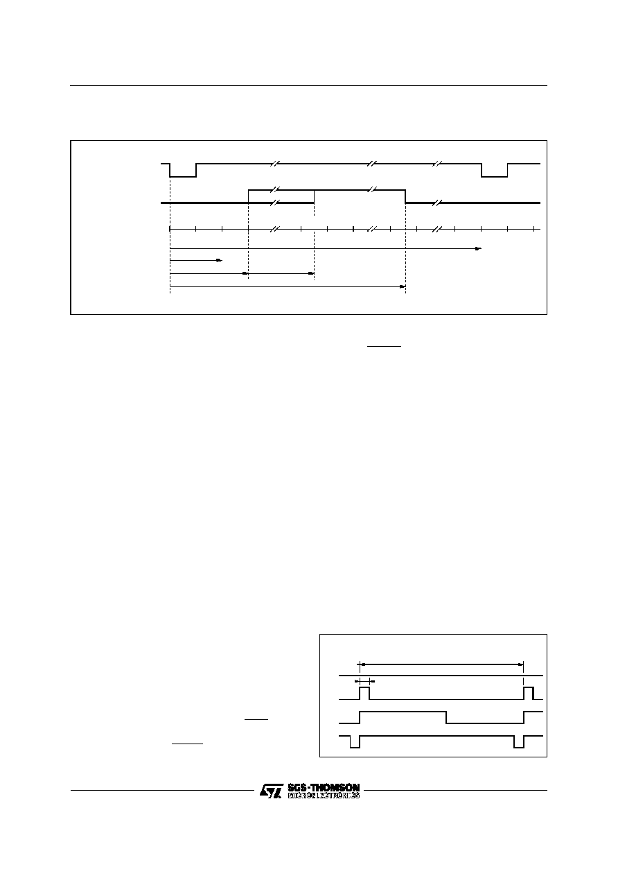
H-SYNC
0
1
2
3
n + 1
n + 2
n + 3
n + 4
LD - 1
LD
0
1
Character
Period
R, G, B
LD[5:0]
Fixed
DD[7:0]
= 4 (min)
= 4n + 2
Given by number
of characters of the strips
9422-07.AI
Figure 5 : Horizontal Timing
IV - Clock and Timing
The whole timing is derived from the XTALIN and the
SYNCHRO (horizontal and vertival) input frequen-
cies. The XTALIN input frequencycan be an external
clock or a crystal signal thanks to XTALIN/XTALOUT
pins. The value of this frequency can be chosen
between 8 and 15MHz, it is available on the CKOUT
pin and is used by the PLL to generate a pixel clock
locked on the horizontal synchro input signal.
IV.1 - Horizontal Timing (see Figure 5)
The number of pixel periods is given by the LINE
DURATION register and is equal to :
[LD[5:0] + 1 ] x 12.
(LD[5:0] : value of the LINE DURATION register).
This value allows to choose the horizontal size of the
characters. The horizontal left margin is given by the
HORIZONTAL DELAY register and is equal to :
[DD[7:0] + 8] x 3 x T
PXCK
(DD[7:0] : value of the DISPLAY DELAY register
and T
PXCK
: pixel period).
This value allows to choose the horizontal position
of the characters on the screen. The value of
DD[7:0] must be equal or greater than 4 (the mini-
mum value of the horizontal delay is 36 x T
PXCK
= 3
character periods). The length of the active area,
where R, G, B are different from 0, depends on the
number of characters of the strips.
IV.2 - D to A Timing (STV9422)
The D to A converters of the STV9422 are pulse
width modulater converter.
The frequency of the output signal is :
f
XTAL
256
and the duty cycle is :
Vi[7:0]
256
per cent.
After a low pass filter, the average value of the
output is :
Vi [7:0]
256
V
DD
V - Display Control
A screen is composed of successive scanlines gath-
ered in several strips. Each strip is defined by a
descriptor stored in memory. A table of descriptors
allows screen composition and different tables can
be stored in memory at the page addresses (8 pos-
sible
addresses).
Two types of strips are available :
- Spacing strip : its descriptor (see II) gives the
number of black (FBK = 1 in DISPLAY CONTROL
register) or transparent (FBK = 0) lines.
- Character strip : its descriptor gives the memory
address of the character codes corresponding to
the 1st displayed character. The characters and
attributes (see code format III) are defined by a
succession of codes stored in the RAM at ad-
dresses starting from the 1st one given by the
descriptor. A character strip can be displayed or
not by using the DE bit of its descriptor. A zoom
can be made on it by using the ZY bit.
0
1
128
255
V1[7:0]
256 . t
XTAL
P WM1 Signa l
t
XTAL
9422-08.EPS
Figure 6 : PWM Timing
STV9422 - STV9424
9/15
FUNCTIONAL DESCRIPTION (continued)
After the falling edge on V-SYNC, the first strip
descriptor is read at the top of the current table of
descriptors at the address given by P[9:0] (see
DISPLAY CONTROL register).
If it is a spacing strip, SL[7:0] black or transparent
scan lines are displayed.
If it is a character strip, during CH[5:0] x (I + ZY)
scan lines (CH[5:0] given by the CHARACTER
HEIGHT register), the character codes are read at
the addresses starting from the 1
st
one given by the
descriptor until a end of line character or the end of
the scan line.
The next descriptor is then read and the same proc-
ess is repeated until the next falling edgeon V-SYNC.
CSD FBK FL[1:0]
P8
P7
P8
DISPLAY CONTROL Register
TABLE OF THE
DESCRIPTORS
2nd CHARACTER
STRIP CODES
OTHER
TABLE OF
DESCRIPTORS
OTHER
(UDC for example)
1st CHARACTER
STRIP CODES
3rd CHARACTER
SRTIP CODES
OTHER
(CODES OR
DESCRIPTORS)
SPACING
ROW1
ROW2
SPACING
ROW3
SPACING
RAM CODE
AND DESCRIPTORS
V-SYNC
TOP SPACING STRIP
1st CHARACTER STRIP
2nd CHARACTER STRIP
3rd CHARACTER STRIP
SPACING STRIP
|
BOTTOM SPACING STRIP
SCREEN
9422-09.EPS
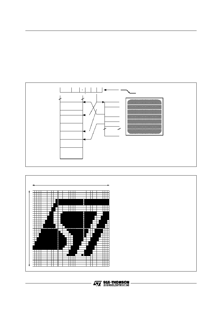
Figure 7 : Relation between Screen/Address Page/Character Code in RAM
Slice 18 of the character n
∞
2
only for vertical shadowing
(not displayed).
1
2
3
4
5
6
7
8
9
10
11
12
13
14
15
16
17
18
1
2
3
1
2
3
4
5
6
7
8
9
10
11
12
13
14
15
16
17
18
4
5
6
36 Pixels (= 3 Characters)
36
Slices
(=
2
Characters)
Character Number
Character Number
ON THE SCREEN
(example for Character n
∞
5)
IN THE RAM
Slice 0
Slice 1
Slice 2
Slice 3
Slice 4
Slice 5
Slice 6
Slice 7
Slice 8
Slice 9
Slice 10
Slice 11
Slice 12
Slice 13
Slice 14
Slice 15
Slice 16
Slice 17
Slice 18
: 0x01
: 0x00
: 0x08
: 0x0c
: 0x0e
: 0x0f
: 0x0f
: 0x0f
: 0x0f
: 0x0e
: 0x0c
: 0x00
: 0x00
: 0x00
: 0x00
: 0x00
: 0x00
: 0x00
: 0x00
0xff =
0xff
0x7f
0x3f
0x1f
0x1f
0x1f
0x1e
0x1e
0x3c
0x3c
0x78
0x78
0xf1
0x00
0x00
0x00
0x00
0x00
Odd
Address
Even
Address
9422-10.AI
Figure 8 : User Definable Character
STV9422 - STV9424
10/15
FUNCTIONAL DESCRIPTION (continued)
8
9
a
b
c
d
e
f
0
1
2
3
4
5
6
7
0
1
2
3
C(6:4)
C(3:0)
CHARACTER NUMBER C(6:0)
4
5
6
7
9422-11.EPS
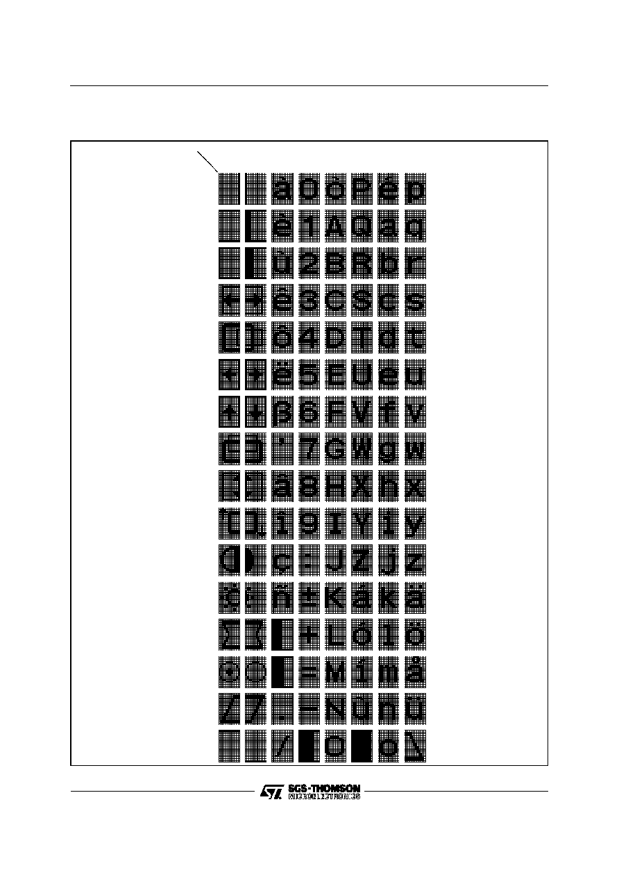
Table 1 : ROM Character Generator
STV9422 - STV9424
11/15
FUNCTIONAL DESCRIPTION (continued)
VI - User Definable Character
The STV9422/24 allows the user to dynamically
define character(s) for his own needs (for a special
LOGO for example). Like the ROM characters, a
UDC is made of a 12 pixels x 18 slices dot matrix,
but one more slice is added for the vertical shad-
owing when several UDCs are gathered to make a
special great character (see Figure 8).
In a UDC, each pixel is defined with a bit, 1 refers
to foreground, and 0 to background color. Each
slice of a UDC uses 2 bytes :
add +
1
-
-
-
-
PX11 PX10 PX9
PX8
add
(even)
PX7 PX6 PX5 PX4 PX3 PX2 PX1 PX0
PX11 is the left most pixel. Character slice address :
SLICE ADDRESS = 38 x (CHARACTER NUMBER)
+ (SLICE NUMBER).
Where :
- CHARACTER NUMBER is the number given by
the character code,
- SLICE NUMBER is the number given by the slice
interpolator (n
∞
of the current slice of the strip :
1 < <18)
VII - ROM Character Generator
The STV9422/24 includes a ROM character gen-
erator which is made of 128 alphanumeric or
graphic characters (see Table 1)
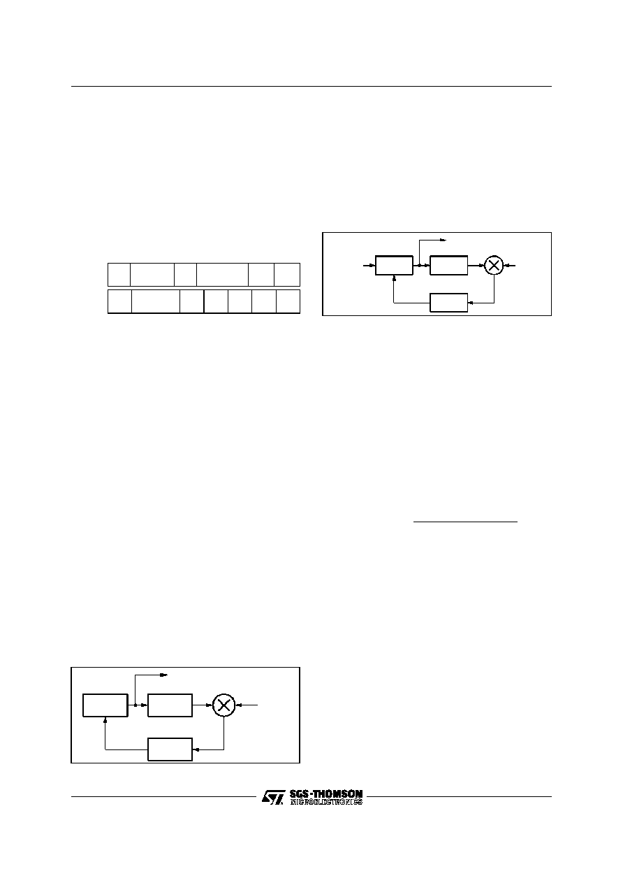
VIII - PLL
The PLL function of the STV9422/24 provides the
internal pixel clock locked on the horizontal synchro
signal and used by the display processor to gener-
ate the R, G, B and fast blanckingsignals. It is made
of 2 PLLs. The first one analogic (see Figure 9),
provides a high frequency signal locked on the
crystal frequency. The frequency multiplier is given
by :
N = 2
(FM[3:0] + 3)
Where FM[3:0] is the value of the FREQUENCY
MULTIPLIER register.
FILTRE
%N
F
XTAL
VCO
N . F
XTAL
9422-12.AI
Figure 9 : Analogic PLL
The second PLL, full digital (see Figure 10), pro-
vides a pixel frequency locked on the horizontal
synchro signal. The ratio between the frequencies
of these 2 signals is :
M = 12 x (LD[5:0] + 1)
Where LD[5:0] is the value of the LINE DURATION
register.
ALGO
%M
F
H-SYNC
%D
M . F
H-SYNC
err(n)
D(n)
N . F
XTAL
9422-13.AI
Figure 10 : Digital PLL
VIII.1 - Programming of the PLL Registers
Frequency Multiplier (@3FF7)
This register gives the ratio between the crystal
frequency and the high frequency of the signal
used by the 2
nd
PLLto provide, by division, the pixel
clock. The value of this high frequency must be
near to 200MHz (for example if the crystal is a
8MHz, the value of FM must be equal to 10) and
greater than 6 x (pixel frequency).
Initial Pixel Period (@3FF6)
This register allows to increase the speed of the
convergence of the PLL when the horizontal fre-
quency changes (new graphic standart). The rela-
tionship between FM[3:0], PP[7:0], LD[5:0], F
HSYNC
and F
XTAL
is :
PP[7:0]
=
round
8
2
(
FM[3:0]
+
3
)
F
XTAL
12
(
LD[5:0]
+
1
)
F
HSYNC
±
24
Locking Condition Time Constant (@ 3FF4)
This register gives the constants AS[2:0] and
BS[2:0] used by the algo part of the PLL (see Figure
10) to calculate, from the phase error, err(n), the
new value, D(n), of the division of the high fre-
quency signal to provide the pixel clock. These two
constants are used only in locking condition, which
is true, if the phase error is less than a fixed value
during at least, 4 scan lines. If the phase error
becomes greater than the fixed value, the PLL is
not in locking condition but in capture process. In
this case, the algo part of the PLL used the other
constants, AF[2:0] and BF[2:0], given by the next
register.
Capture Process Time Constant (@ 3FF5)
The choice between these two time constants
(locking condition or capture process) allows to
decrease the capture process time by changing the
time response of the PLL.
STV9422 - STV9424
12/15
FUNCTIONAL DESCRIPTION (continued)
VIII.2 - How to choose the value of the time
constant ?
The time response of the PLL is given by its char-
acteristic equation which is :
(
x
±
1
)
2
+ ( + ) (
x
±
1
) + =
0.
Where :
=
3
LD[5:0]
2
A
±
11
and
=
3
LD[5:0]
2
B
±
19
.
(LD[5:0] = value of the LINE DURATION register,
A = value of the 1st time constant, AF or AS and
B = value of the 2
d
time constant, BF or BS).
As you can see, the solution depend only on the
LINE DURATION and the TIME CONSTANTS
given by the I
2
C registers.
If
( + )
2
±
4
0 and 2
± <
4, the PLL is sta-
ble
and its response is like this presented on
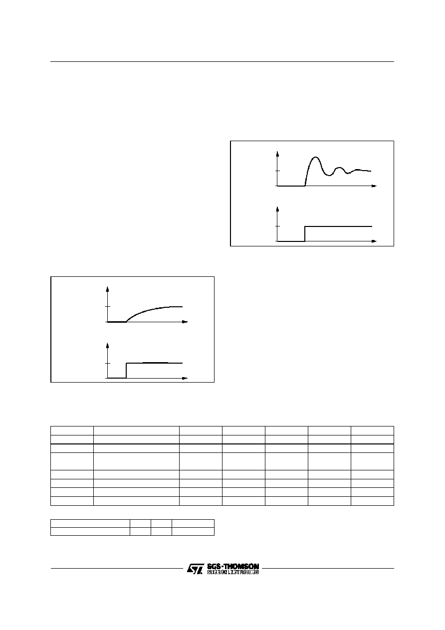
Figure 11.
t
PLL
Frequency
f
0
f
1
t
Input
Frequency
f
0
f
1
9422-14.AI
Figure 11 : Time Response of the PLL/Charac-
teristic Equation Solutions (with
Real Solutions)
If
( + )
2
±
4
0, the response of the PLL is like
this presented on Figure 12.
In this case the PLL is stable if
> 0.7 damping
coefficient).
t
PLL
Frequency
f
0
f
1
t
Input
Frequency
f
0
f
1
9422-15.AI
Figure 12 : Time Response of the PLL/Charac-
teristic Equation Solutions (with
Complex Solutions)
The Table 2 gives some good values for A and B
constants for different values of the LINE DURA-
TION.
Summary
For a good working of the PLL :
- A and B time constants must be chosen among
values for which the PLL is stable,
- B must be equal or greater than A and the differ-
ence between them must be less than 3,
- The greater (A, B) are, the faster the capture is.
An optimal choice for the most of applications might
be :
- For locking condition : AS = 0 and BS = 1,
- For capture process : AS = 2 and BS = 4.
But for each application the time constants can be
calculated by solving the characteristic equation
and choosing the best response.
Table 2 : Valid Time Constants Examples
B \ A
0
1
2
3
4
5
6
0
YYYY
YYYY
YYYY
YYYN
YNNN
NNNN
NNNN
1
YYYY
YYYY
YYYY
YYYN
YNNN
NNNN
NNNN
2
NYYY
YYYY
YYYY
YYYN
YNNN
NNNN
NNNN
3
NNNY
YYYY
YYYY
YYYN
YNNN
NNNN
NNNN
4
NNNN
NYYY
(1)
YYYY
YYYN
YNNN
NNNN
NNNN
5
NNNN
NNNY
YYYY
YYYN
YNNN
NNNN
NNNN
6
NNNN
NNNN
NYYY
YYYN
YNNN
NNNN
NNNN
7
NNNN
NNNN
NNNY
YYYN
YNNN
NNNN
NNNN
9422-05.TBL
Note : 1. Case of A[2:0] = 1 (001) and B[2:0] = 4 (100) :
LD
16
32
48
63
Valid Time Constants
N
Y
Y
Y
Value of LINE DURATION Register (@ 3FF0) :
LD = 16 : LD[5:0] = 010000
LD = 32 : LD[5:0] = 100000
LD = 48 : LD[5:0] = 110000
LD = 63 : LD[5:0] = 111111
Table meaning :
N = No possible capture
Y = PLL can lock
STV9422 - STV9424
13/15
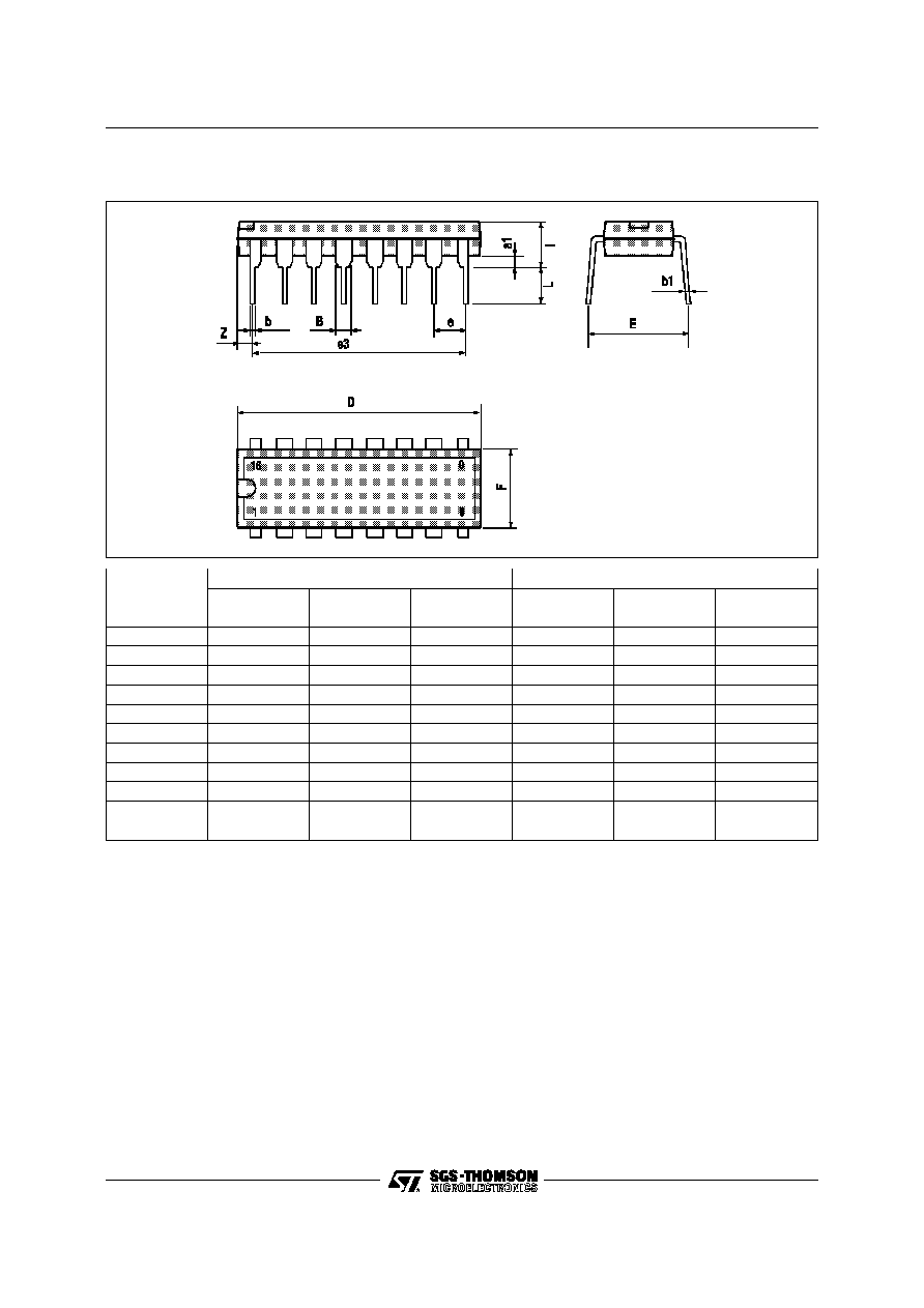
PM-DIP16.WMF
PACKAGE MECHANICAL DATA (STV9424)
16 PINS - PLASTIC DIP
Dimensions
Millimeters
Inches
Min.
Typ.
Max.
Min.
Typ.
Max.
a1
0.51
0.020
B
0.77
1.65
0.030
0.065
b
0.5
0.020
b1
0.25
0.010
D
20
0.787
E
8.5
0.335
e
2.54
0.100
e3
17.78
0.700
F
7.1
0.280
I
5.1
0.201
L
3.3
0.130
Z
1.27
0.050
DIP16.TBL
STV9422 - STV9424
14/15
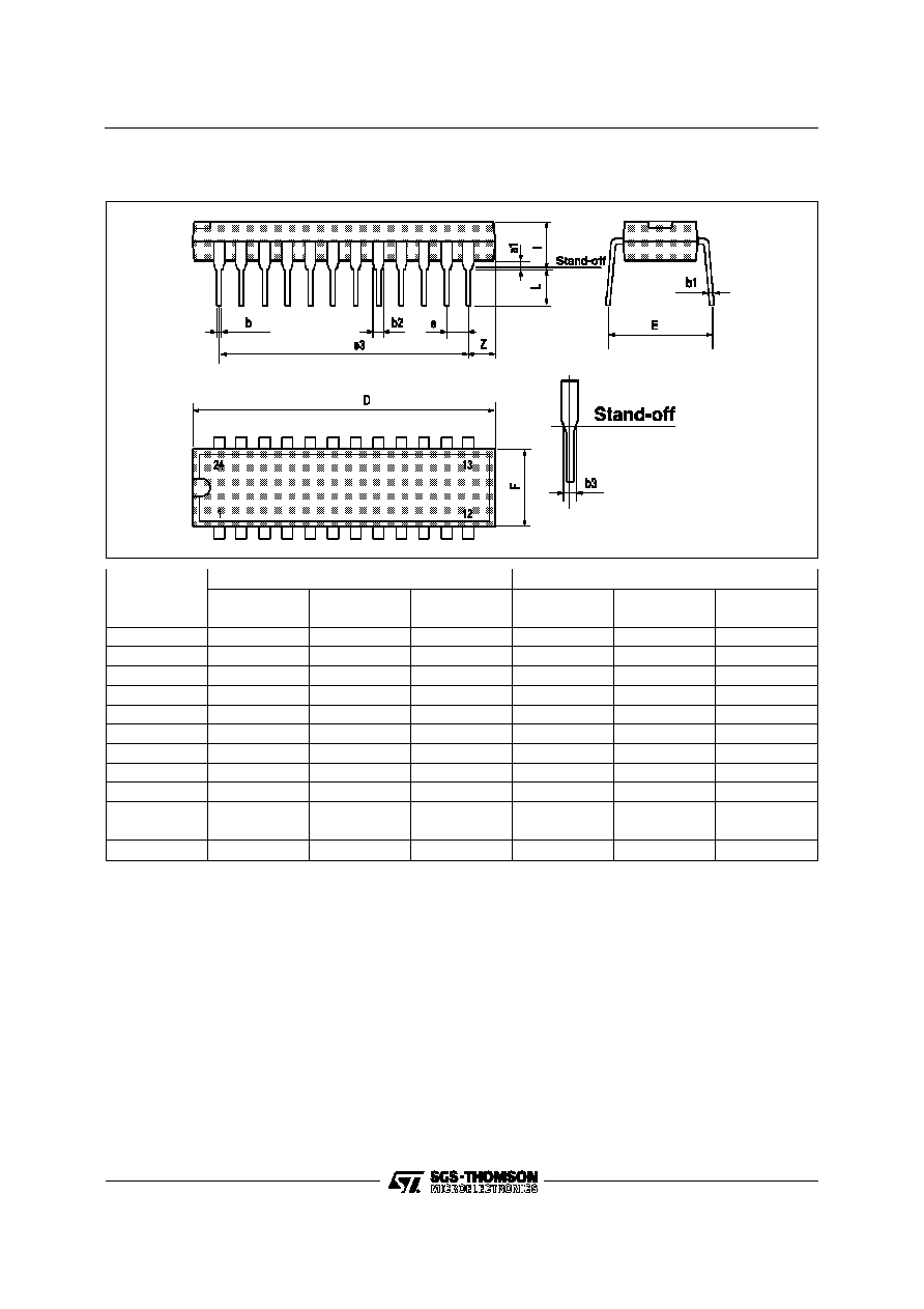
PMSDIP24.WMF
PACKAGE MECHANICAL DATA (STV9422)
24 PINS - PLASTIC SHRINK DIP
Dimensions
Millimeters
Inches
Min.
Typ.
Max.
Min.
Typ.
Max.
a1
0.51
0.020
b
0.36
0.46
0.56
0.0142
0.0181
0.0220
b1
0.23
0.25
0.38
0.0090
0.0098
0.0150
b2
0.76
1.02
1.4
0.030
0.040
0.045
b3
0.76
1.02
1.4
0.030
0.040
0.045
D
22.61
22.86
23.11
0.890
0.90
0.910
E
7.62
8.64
0.30
0.340
e
1.778
0.070
e3
19.558
0.770
e4
7.62
0.300
F
6.10
6.40
6.86
0.240
0.252
0270
I
5.08
0.200
L
2.54
3.30
3.81
0.10
0.130
0.150
SDIP24.TBL
Information furnished is believed to be accurate and reliable. However, SGS-THOMSON Microelectronics assumes no responsibility
for the consequences of use of such information nor for any infringement of patents or other rights of third parties which may result
from its use. No licence is granted by implication or otherwise under any patent or patent rights of SGS-THOMSON Microelectronics.
Specifications mentioned in this publication are subject to change without notice. This publication supersedes and replaces all
information previously supplied. SGS-THOMSON Microelectronics products are not authorized for use as critical components in life
support devices or systems without express written approval of SGS-THOMSON Microelectronics.
©
1995 SGS-THOMSON Microelectronics - All Rights Reserved
Purchase of I
2
C Components of SGS-THOMSON Microelectronics, conveys a license under the Philips
I
2
C Patent. Rights to use these components in a I
2
C system, is granted provided that the system conforms to
the I
2
C Standard Specifications as defined by Philips.
SGS-THOMSON Microelectronics GROUP OF COMPANIES
Australia - Brazil - China - France - Germany - Hong Kong - Italy - Japan - Korea - Malaysia - Malta - Morocco
The Netherlands - Singapore - Spain - Sweden - Switzerland - Taiwan - Thailand - United Kingdom - U.S.A.
STV9422 - STV9424
15/15