STV942x
EVALUATION KIT
OSD FOR MONITORS
April 1995
94
2X
.
T
I
F
I - INTRODUCTION
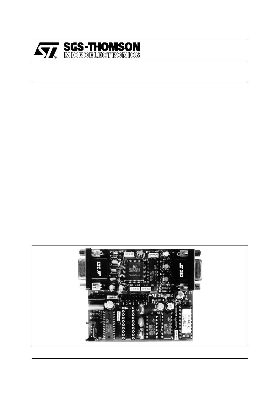
I.1 - Demo Kit Contents
The STV942x OSD for monitors Demo Kit comes
with the following parts :
- The STV942x Demo Board,
- The I
2
C Interface Board,
- One I
2
C Bus Cord,
- One VGA Cord,
- One 3.5" Floppy Containing the Page Editor Soft-
ware,
- The Demo Kit User's Manual.
I.2 - Minimum Hardware and Software
Configuration
The Page Editor Software is delivered on a
MS DOS 3.5" floppy disk.
It requires a PC compatible microcomputer :
- Based on a 486 microprocessor or better,
- With at least 640k of memory.
Use of a 386 or smaller microprocessor will just give
long execution time.
I.3 - How to Get Started
Even if it isn't necessary to connect the application
board to run the Page Editor Software, it will always
be helpful to see the real resulting page on the
application monitor screen.
You may use the Demo Kit for an evaluation pur-
pose, or for developing your OSD pages for your
application. The STV942x Demo Board is supplied
with VGA connectors and it comes with a VGA cord.
The STV942x devices can handle a wide variety of
monitors and video standards. If you are using the
STV942x Demo Kit for evaluating the devices, or
for developing a VGA monitor application, you will
find it is perfectly suited for those purposes. If you
use the kit to develop a non-VGA compatible moni-
tor, you will find the different signals on the connec-
tors and you will have to provide the appropriate
connections to your application. Refer to the
STV942x Demo Board Section.
Connect the I
2
C interface board on the parallel port
LPT1 of your PC, then connect the I
2
C interface
board to the STV942x Demo Board using the I
2
C
bus wire, supply the Demo Board with a 5V power
supply (not provided), and connect the Monitor to
the Demo Board output connector J6, and the PC
video output to the input connector J5, using the
VGA cable provided with the Demo kit.
After having made a copy of the Page Editor Soft-
ware under a working directory of you hard disk,
you can start the execution by typing the com-
mand : STV942X.exe.
1/9
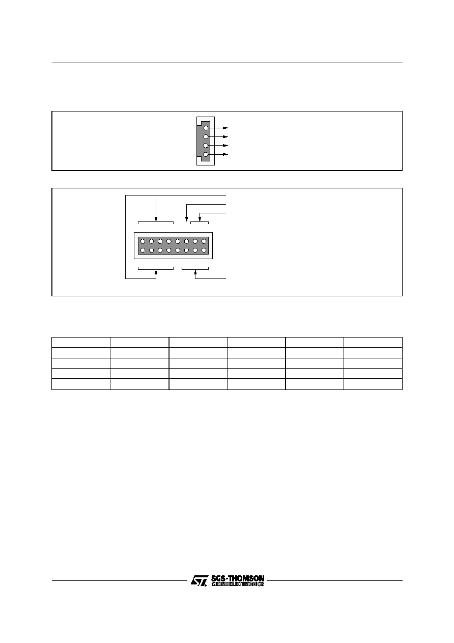
Pin 1 : 5V
Pin 2 : Clock
Pin 3 : Data
Pin 4 : GND
J1
9
4
2
X-0
1
.
EPS
Figure 1 : J1 : I
2
C Connector
II - STV942x DEMO BOARD
II.1 - Connectors
1
J2
3 5 7
K D C
0 2 4 6
R G B
Refers to "R, G, B" output signals
Refers to I
2
C data and clock signals
Refers to PWM outputs
Refers to fast blanking "FBLK" signal
Note : The two unmarked pins are connected to ground
9
4
2
X
-0
2
.
EP
S
Figure 2 : J2 : OSD Signals Test Points
J3 : Power Supply +5V
�
5%
J4 : Power Supply Ground
J5 : VGA, to Video Source
J6 : VGA, to Target Monitor
Table 1 : J5 and J6 Pin Description
Pin 1
Red
Pin 6
GND
Pin 11
NC
Pin 2
Green
Pin 7
GND
Pin 12
NC
Pin 3
Blue
Pin 8
GND
Pin 13
H SYNC
Pin 4
NC
Pin 9
NC
Pin 14
V SYNC
Pin 5
GND
Pin 10
GND
Pin 15
NC
STV942x - DEMO KIT
2/9
1
2
3
4
5
6
7
8
9
10
11
12
24
23
22
21
20
19
18
17
16
15
14
13
PWM0
PWM1
FBLK
VSYNC
HSYNC
V
DD
PXCK
CKOUT
EXTAL
XTAL
PWM2
PWM3
PWM7
PWM6
TEST
B
G
R
V
SS
RES
SDA
SCL
PWM5
PWM4
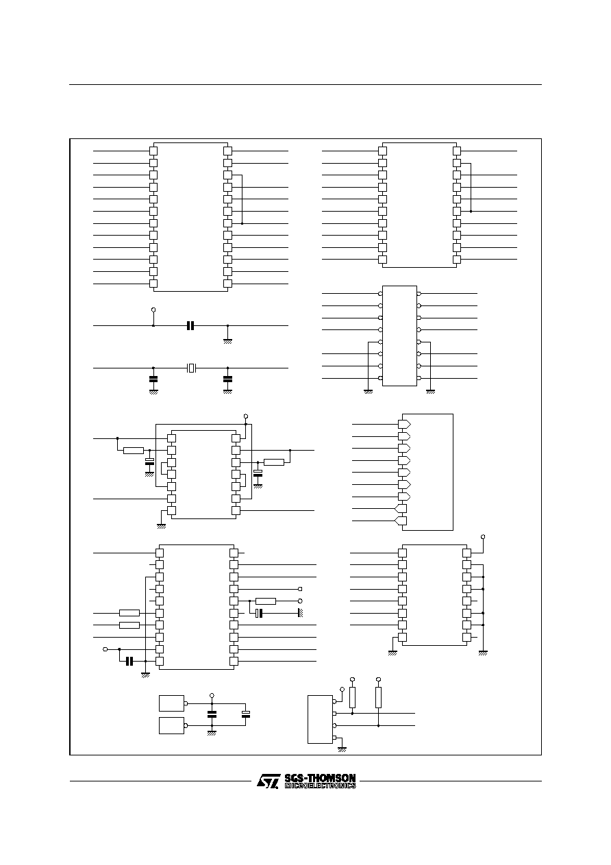
U2
STV9422
OSD_PWM0
OSD_PWM1
OSD_FBLK
OSD_VS
OSD_HS
OSD_VDD
OSD_PXCK
OSD_CKOUT
OSD_EXTAL
OSD_XTAL
OSD_PWM2
OSD_PWM3
OSD_PWM7
OSD_PWM6
OSD_B
OSD_G
OSD_R
OSD_VSS
RES2
OSD_SDA
OSD_SCL
OSD_PWM5
OSD_PWM4
1
2
3
4
5
6
7
8
9
10
11
12
20
19
18
17
16
15
14
13
PWM0
FBLK
VSYNC
HSYNC
V
DD
PXCK
CKOUT
EXTAL
XTAL
PWM3
PWM2
TEST
B
G
R
V
SS
RES
SDA
SCL
PWM1
U1
STV9421
OSD_PWM0
OSD_FBLK
OSD_VS
OSD_HS
OSD_VDD
OSD_PXCK
OSD_CKOUT
OSD_EXTAL
OSD_XTAL
OSD_PWM3
OSD_PWM2
OSD_B
OSD_G
OSD_R
OSD_VSS
RES1
OSD_SDA
OSD_SCL
OSD_PWM1
1
3
7
5
9
11
13
15
J2
2
4
8
6
10
12
14
16
OSD_PWM0
OSD_PWM2
OSD_PWM4
OSD_PWM6
OSD_R
OSD_G
OSD_B
OSD_PWM1
OSD_PWM3
OSD_PWM5
OSD_PWM7
OSD_FBLK
OSD_SDA
OSD_SCL
OSD_VDD
OSD_VSS
C3 100nF
V
CC
GND
OSD_XTAL
OSD_EXTAL
GND
GND
Q1 8MHz
C5
22pF
C4
22pF
1
2
3
4
5
6
7
8
9
10
11
12
14
13
A1
A2
B1
A3
B2
B3
GND
V
CC
D1
C2
D3
C1
C2
C3
U3
74HC86
HS_OUT
OSD_VS
VS_OUT
R3 1k
1
2
3
4
5
6
7
8
9
10
11
12
20
19
18
17
16
15
14
13
PB0
PB1
PB2
TEST
PB3
PB6
PB7
PA0
V
DD
V
SS
PC2
PC3
PC4
NMI
RST
EXTAL
XTAL
PA3
PA2
PA1
U4
ST6260
EXT_SYNC
MCU_VS
MCU_HS
HS_IN
OSD_SDA
OSD_CKOUT
RES1
VS_IN
OSD_SCL
C1 100nF
V
CC
RES2
C2 10�F 9V
R2 47k
GND
GND
V
CC
V
CC
R9 330
R10 330
GND
C6
10�F
GND
OSD_HS
C7
10�F
GND
R4 1k
V
CC
OSD_R
OSD_G
OSD_B
OSD_FBLK
OSD_PXCK
HS_OUT
VS_OUT
HS_IN
VS_IN
OSD_G
OSD_B
OSD_FBLK
OSD_PXCK
HS_OUT
VS_OUT
HS_IN
VS_IN
OSD_R
VGA INTERFACE
1
2
3
4
5
6
7
8
9
10
11
12
14
13
A/B
1A
1Y
1B
2A
2B
2Y
V
DD
G
4A
4B
4Y
3A
3B
U5
74HC157
EXT_SYNC
GND
V
CC
15
16
GND
3Y
MCU_HS
HS_IN
HS_OUT
MCU_VS
VS_IN
VS_OUT
GND
J1
I
2
C
3
4
OSD_SDA
2
1
R5
2.2k
V
CC
GND
V
CC
R1
2.2k
V
CC
OSD_SCL
J3
V
CC
C8
100nF
C9
470�F
J4
GND
5V Power Supply
9
4
2
X-0
3
.
E
P
S
Figure 3
II.2 - Circuit Diagram
STV942x - DEMO KIT
3/9
1
2
3
4
5
6
7
8
9
10
11
12
14
13
I1
O2
O2
I2
I3
O3
GND
V
CC
I6
O6
I5
O5
I4
O4
U7
74HC04
C22
100nF
GND
V
CC
OSD_FBLK
BLANK
OSD_PXCK
CLOCK
1
2
3
4
5
6
7
8
9
10
11
12
20
19
18
17
16
15
14
13
R1
21
22
R0
DV
CC
DGND
AV
CC
AGND
NC
ROUT
RAUX
AGND
GOUT
GAUX
44
36
37
38
39
40
41
42
43
35
34
G4
G5
G6
G7
COM
NC
CLK
R/C
B0
B1
B2
R2
R3
R4
R5
R6
R7
G0
G1
G2
G3
33
32
31
30
29
28
27
26
25
24
23
AGND
BOUT
BAUX
AV
CC
DGND
DV
CC
B7
B6
B5
B4
B3
U6
STV8438
BLANK
CLOCK
OSD_B
GND
V
CC
C11
4.7nF
C10
47�F
C13
4.7nF
C12
47�F
B_VGA_OUT
B_VGA_IN
G_VGA_IN
G_VGA_OUT
R_VGA_IN
R_VGA_OUT
C15
4.7nF
C14
47�F
GND
V
CC
V
CC
OSD_G
OSD_R
C18 1�F
R13
1k
HS_IN
15
5
10
14
4
9
13
3
8
12
2
7
11
1
6
R14
1k
GND
GND
R20
75
R19
75
GND
R18
75
C17 1�F
G_VGA_IN
R_VGA_IN
C16 1�F
B_VGA_IN
VS_IN
J5
VGA IN
R17 75
C21 47�F
HS_OUT
15
5
10
14
4
9
13
3
8
12
2
7
11
1
6
GND
GND
G_VGA_OUT
R_VGA_OUT
B_VGA_OUT
VS_OUT
J6
VGA OUT
R16 75
R15 75
C20 47�F
C19 47�F
2.2k
2.2k
220pF
220pF
9
4
2
X-0
4
.
EPS
Figure 4
STV942x - DEMO KIT
4/9
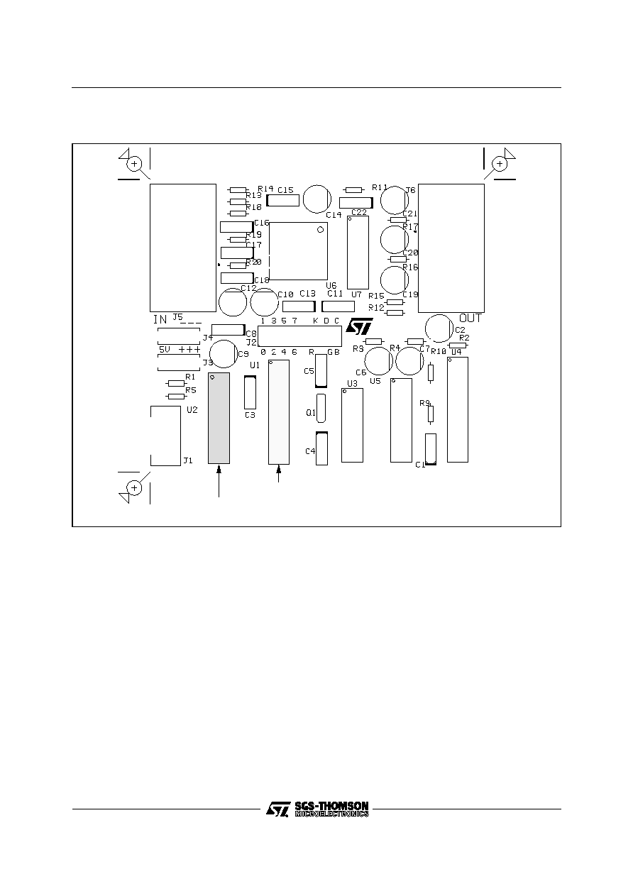
II.3 - Board Layout
JB04BX
Connected
to Target Monitor
(PC Monitor)
Connected
to Video Source
(PC Video Board)
Connected
to I
2
C Interface
Board
Socket for STV9422
Socket for STV9421
Note : Only ONE OSD must be installed on board.
9
4
2
X-0
5
.
EPS
Figure 5
II.4 - Demo Board Operation
The STV942x Demo board is designed to be in-
serted into a VGA connection.
The video signals generated by the OSD device are
mixed with the incoming video signals at the input
connector J5. The combination of both signals is
available on the output connector J6. The mixing is
done with the video switch/triple DAC : STV8438.
This device provides a triple analog video input, a
triple digital video input, a video switch and three
buffers for 75
drive. It operates at 100MHz on the
analog input and on the video switch, and up to
70MHz on the digital inputs. In this application, the
three 8 bits converters are used as 3 single bit
converters as the OSD provides 1 bit RGB signals.
A ST6 micro controller gives the board the ability
to run a small stand-alone demo program : It deliv-
ers two Horizontal and vertical synchronization sig-
nals, at about 31kHz and 60Hz, and drives the OSD
I
2
C bus. As soon as an external sync is detected on
the input VGA connector, the mcu stops delivering
its own sync and it transmits the input sync signals
to the VGA output connector. In a same manner, as
soon as the mcu detects an external master on the
I
2
C bus, it stops driving its demo program.
The Demo board can be equipped either with a
STV9421 OSD (on socket U1), or with a STV9422
OSD (on socket U2) Never put both OSDs on the
board at the same time !!
STV942x - DEMO KIT
5/9