This is preliminary information on a new product in development or undergoing evaluation. Details are subject to change without notice.
Rev. 4.0
February 2000
1/24
STV9432TA
100MHz OSD FOR MONITOR
INCLUDING BEAM CURRENTS & VIDEO TIMING ANALYZER
∑ MULTIFUNCTION OSD FOR MONITOR
∑ INCLUDES FACILITIES FOR CUT-OFF VOLT-
AGES MONITORING:
- THREE 8 BITS ADC INPUTS
- ADC TRIGGER DURING RETRACE TIME OF A
PROGRAMMED LINE
∑ INCLUDES FACILITIES FOR SCREEN SIZE &
CENTERING AUTO SETUP
- HS, VS, VIDEO TIMING MEASUREMENTS
∑ 100MHz MAX. PIXEL CLOCK, AVAILABLE FOR
ANY LINE FREQUENCY BETWEEN 15 AND
140 kHz
∑ 12 x 18 CHARACTER ROM FONT INCLUDES:
- 240 MONOCOLOR CHARACTERS
- 16 MULTICOLOR CHARACTERS
∑ CHARACTER FLASHING
∑ UP TO 1K CHARACTERS TEXT DISPLAY
∑ ULTRA HIGH FREQUENCY PLL FOR JITTER-
FREE DISPLAY
∑ FLEXIBLE DISPLAY:
- ANY CHARACTER WIDTH AND HEIGHT
- ANYWHERE IN THE SCREEN
∑ SINGLE BYTE CHARACTER CODES AND
COLOR LOOK-UP TABLE FOR EASY PRO-
GRAMMING AND FAST ACCESS
∑ CHARACTER FLIP OPERATIONS
∑ WIDE DISPLAY WINDOW ALLOWS PATTERN
GENERATION FOR FACTORY ADJUSTMENTS
∑ I
2
C BUS MCU INTERFACE
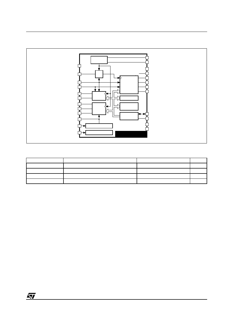
DESCRIPTION
Connected to a host MCU via a serial I
2
C Bus, the
STV9432TA is a multifunction slave peripheral device
integrating the following blocks:
- On-screen Display. It includes a MASK PRO-
GRAMMABLE ROM that holds the CUSTOM
CHARACTER FONT, a 1Kbytes RAM that stores
the code strings of the different lines of text to be
displayed, and a set of registers to program char-
acter sizes and colors. A built-in digital PLL, oper-
ating at very high frequency, provides an accurate
display without visible jitter for a wide line fre-
quency range from 15 to 140 kHz.
- Cut-off Monitoring Circuitry includes 3 x 8 bits
ADCs and a programmable ADC sampling trigger.
It gives the possibility to measure the three beam
currents, during the horizontal flyback, at a given
line in the frame, provided that the three ADC
inputs are connected to a beam current sensing
circuitry. The values are stored in three BEAM
CURRENT REGISTERS, and available for MCU
read.
- Video Timing Analyzer. Using the Horizontal Sync,
Vertical Sync, Horizontal Flyback, and "Video
Active" inputs, a set of counters provide the differ-
ent timing measurements necessary to analyze
the current Video timing characteristics to make
the automatic set-up of screen size and centering.
The measurements are initialized on the same
programmable trigger line than in the above cut-off
monitoring circuitry
PIN CONNECTIONS
SDIP24 (Plastic Package)
ORDER CODE: STV9432TA
1
2
3
4
5
6
7
8
9
10
11
12
20
19
18
17
16
15
14
13
24
23
22
21
RCI
GCI
BCI
ADCREF
AGND
TEST
FILTER
HFLY
AV
DV
DD
DV
S S
ROUT
GOUT
BOUT
FBLK
SDA
SCL
HS
VS
XTI
XTO
OV
S S
OV
DD
AV
DD
1
STV9432TA
4/24
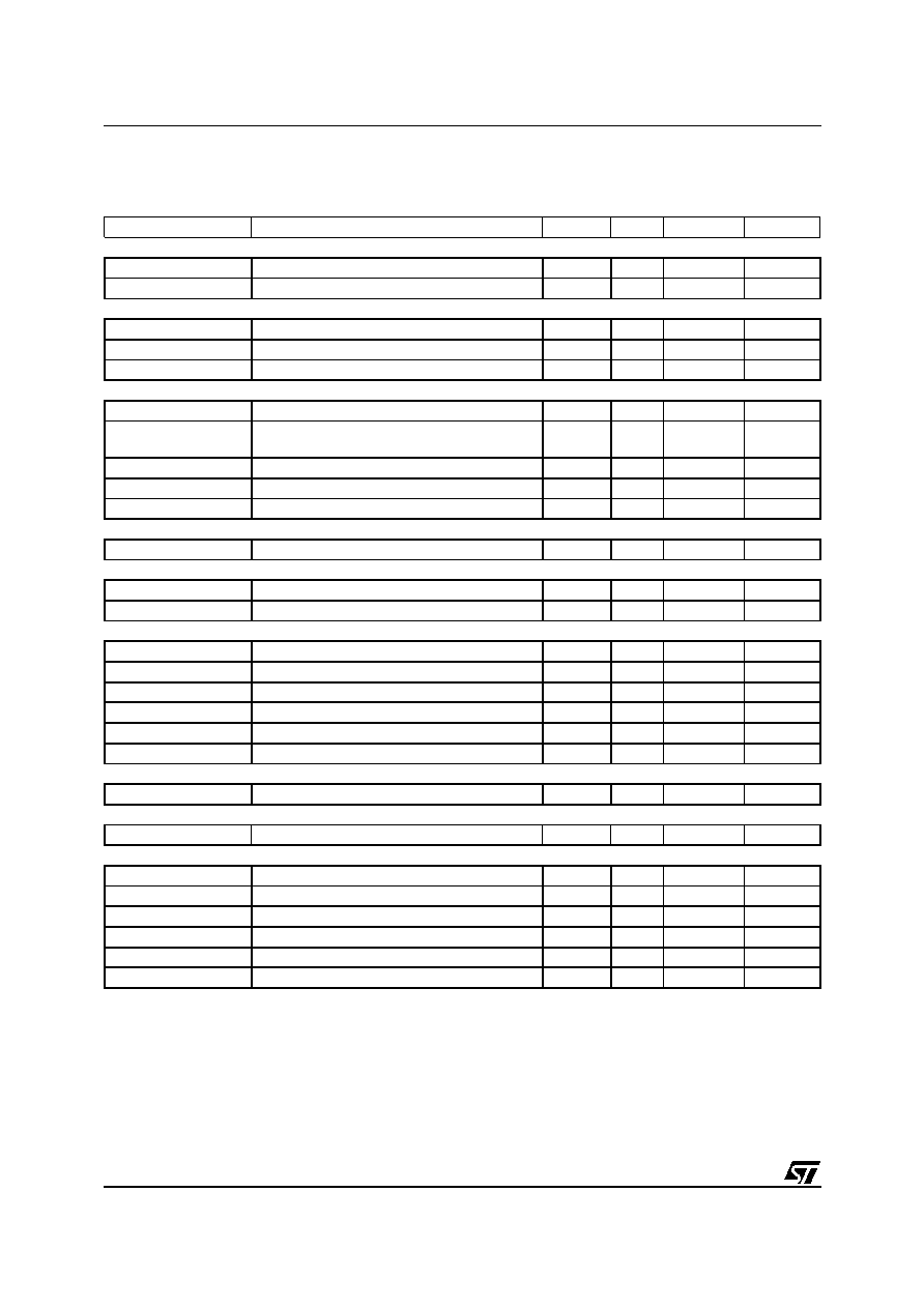
4 - ELECTRICAL CHARACTERISTICS
(V
DD
= 5V, V
SS
= 0V, GND = 0V, T
A
= 0 to 70
o
, unless otherwise specified)
Symbol
Parameter
Min.
Typ.
Max.
Unit
SUPPLY
AV
DD
, DV
DD
, OV
DD
Supply Voltage
4.75
5
5.25
V
AI
DD
+ DI
DD
+ OI
DD
Analog and Digital Supply Current
-
-
150
mA
INPUTS (SCL, SDA)
V
IL
Input Low Voltage
0.8
V
V
IH
Input High Voltage
2.4
V
I
IL
Input Leakage Current
-1
+1
µA
INPUTS (HS, VS, AV, HFLY)
V
IL
Input Low Voltage
0.8
V
V
IH
Input High Voltage
HS, VS, AV
HFLY
2.4
3.6
V
V
HYST
Schmidt Trigger Hysteresis
0.4
V
I
PU
Pull-up Source Current (V
IN
= 0V)
100
µA
HSIN
Horizontal Synchro Input Range
15
140
kHz
OUTPUTS (SDA open drain)
V
OL
Output Low Voltage (I
OL
= 3mA)
0
0.4
V
OUTPUTS (R, G, B, FBLK)
V
OL
Output Low Voltage (I
OL
= 3mA)
0
0.4
V
V
OH
Output High Voltage (I
OH
= 3mA)
0.8V
DD
V
DD
V
OSCILLATOR (XTI, XTO)
I
IL
XTI Input Source Current (V
IN
= 0V)
3
15
µA
I
IH
XTI Input Sink Current (V
IN
= V
DD
)
3
15
µA
V
IL
XTI Input Low Voltage
1.4
V
V
IH
XTI Input High Voltage
0.7V
DD
V
V
OL
XTI Output Low Voltage (I
OL
= 3mA)
0
0.4
V
V
OH
XTI Output High Voltage (I
OH
= 3mA)
0.8V
DD
V
DD
V
ADCREF
V
REF
Output Voltage Reference
3.3
V
POWER-ON RESET
DV
DDTH
Supply Threshold Level
3.6
V
8 BITS ADC INPUTS (RCI GCI BCI)
V
IN
Input Voltage
0
V
ADCREF
V
Z
IN
Input Impedance
100
k
V
OFF
Input Offset Voltage
3
LSB
I
LEAK
Input Leakage Current
0
50
µA
ILE
Integral Linearity Error (Note 2)
-2
+2
LSB
DLE
Differential Linearity Error (Note 2)
-0.5
+0.5
LSB
2
STV9432TA
5/24
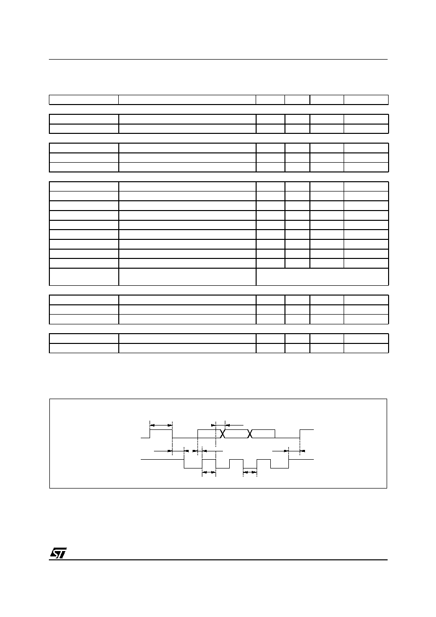
5 - TIMINGS
Note 1: These parameters are not tested on each unit. They are measured during our internal qualification procedure which includes char-
acterization on batches comming from corners of our processes and also temperature characterization
Note 2 : The ADC measurements are dependant on the noise. The test is done by correlation in order to screen out marginal devices.
Note 3 :
t
HTIM
= 3t
OSC
: 40.
Figure 1.
Symbol
Parameter
Min.
Typ.
Max.
Unit
OSCILLATOR
f
OSC
Clock Frequency
8
MHz
f
PXL
Pixel Frequency
100
MHz
R, G, B, FBLK (C
LOAD
= 30pF)
t
R
Rise Time (see Note 1)
5
ns
t
F
Fall Time (see Note 1)
5
ns
t
SKEW
Skew between R, G, B, FBLK
5
ns
I
2
C INTERFACE: SDA AND SCL (see
Figure 1
)
f
SCL
SCL Clock Frequency
0
400
kHz
t
BUF
Time the bus must be free between 2 access
500
ns
t
HDS
Hold Time for Start Condition
500
ns
t
SUP
Set up Time for Stop Condition
500
ns
t
LOW
The Low Period of Clock
400
ns
t
HIGH
The High Period of Clock
400
ns
t
HDAT
Hold Time Data
0
ns
t
SUDAT
Set up Time Data
500
ns
t
F
Fall Time of SDA
20
ns
t
R
Rise Time of both SCL and SDA
Depend on the pull-up resistor and the load
capacitance
ANALYZER (HS, HFLY, AV)
t
HLOW
Low Pulse Width (see Note 3)
2
4091
t
HTIM
t
HHIGH
High Pulse Width (see Note 3)
2
4091
t
HTIM
Hs max
Max Hs Frequency
Hfly
ANALYZER (VS)
t
VLOW
Low Pulse Width
2
4091
Lines
t
VHIGH
High Pulse Width
2
4091
Lines
SDA
SCL
STOP
START
DATA
t
BUF
t
HDAT
t
HDS
t
SUP
t
HIGH
t
LOW
STOP
t
SUDAT
2