February 2002
1/24
Version 4.0
STV9553
12 ns TRIPLE-CHANNEL HIGH VOLTAGE VIDEO AMPLIFIER
FEATURES
s
Triple-channel video amplifier
s
Supply voltage up to 115 V
s
80V Output dynamic range
s
Perfect
for
PICTURE
BOOST
application
requiring high video amplitude
s
Pinning for easy PCB layout
s
Supports DC coupling (optimum cost saving)
and AC coupling applications.
s
Built-in Voltage Gain: 20 (Typ.)
s
Rise and Fall Times: 12 ns (Typ.)
s
Bandwidth: 29 MHz (Typ.)
s
Very low stand-by power consumption
s
Perfectly
matched
with
the
STV921x
preamplifiers
DESCRIPTION
The STV9553 is a triple-channel video amplifier
designed in a 120V-high voltage technology and
able to drive in DC-coupling mode the 3 cathodes
of a CRT monitor.
The
STV9553
supports
PICTURE
BOOST
applications where video amplitude up to 50V or
above is required, ensuring a maximum quality of
the still pictures or moving video.
Perfecly
matched
with
the
STV921x
ST
preamplifiers, it provides a highly performant and
very cost effective video system.
PIN CONNECTIONS
CLIPWATT 11
ORDER CODE: STV9553
(Plastic Package)
1
2
3
4
5
6
7
8
9
10
11
OUT1
OUT2
OUT3
GNDP
GNDA
IN3
V
DD
GNDS
V
CC
IN2
IN1
1

Table of Contents
2
2/24
1
BLOCK DIAGRAM . . . . . . . . . . . . . . . . . . . . . . . . . . . . . . . . . . . . . . . . . . . . . . . . . . . . . . . . . . . 3
2
PIN DESCRIPTION . . . . . . . . . . . . . . . . . . . . . . . . . . . . . . . . . . . . . . . . . . . . . . . . . . . . . . . . . . 3
3
ABSOLUTE MAXIMUM RATINGS . . . . . . . . . . . . . . . . . . . . . . . . . . . . . . . . . . . . . . . . . . . . . . 4
4
THERMAL DATA . . . . . . . . . . . . . . . . . . . . . . . . . . . . . . . . . . . . . . . . . . . . . . . . . . . . . . . . . . . . 4
5
ELECTRICAL CHARACTERISTICS . . . . . . . . . . . . . . . . . . . . . . . . . . . . . . . . . . . . . . . . . . . . . 5
6
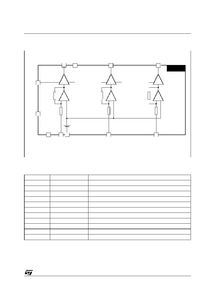
THEORY OF OPERATION . . . . . . . . . . . . . . . . . . . . . . . . . . . . . . . . . . . . . . . . . . . . . . . . . . . . 7
6.1
General . . . . . . . . . . . . . . . . . . . . . . . . . . . . . . . . . . . . . . . . . . . . . . . . . . . . . . . . . . . . . 7
6.2
Output voltage . . . . . . . . . . . . . . . . . . . . . . . . . . . . . . . . . . . . . . . . . . . . . . . . . . . . . . . . 8
7
POWER DISSIPATION . . . . . . . . . . . . . . . . . . . . . . . . . . . . . . . . . . . . . . . . . . . . . . . . . . . . . . . 9
8
TYPICAL PERFORMANCE CHARACTERISTICS . . . . . . . . . . . . . . . . . . . . . . . . . . . . . . . . . 10
9
INTERNAL SCHEMATICS . . . . . . . . . . . . . . . . . . . . . . . . . . . . . . . . . . . . . . . . . . . . . . . . . . . . 11
10 APPLICATION HINTS . . . . . . . . . . . . . . . . . . . . . . . . . . . . . . . . . . . . . . . . . . . . . . . . . . . . . . . 12
10.1
How to choose the high supply voltage value (VDD) in DC coupling mode . . . . . . . . 12
10.2
Arcing Protection: schematics . . . . . . . . . . . . . . . . . . . . . . . . . . . . . . . . . . . . . . . . . . . 12
10.3
Arcing protection: layout and decoupling . . . . . . . . . . . . . . . . . . . . . . . . . . . . . . . . . . . 13
10.4
Video response optimization: schematics in DC-coupling mode . . . . . . . . . . . . . . . . . 14
10.5
Video response optimization: outputs networks . . . . . . . . . . . . . . . . . . . . . . . . . . . . . . 15
10.6
Video response optimization: inputs networks . . . . . . . . . . . . . . . . . . . . . . . . . . . . . . . 15
10.7
Video response optimization: layout and decoupling . . . . . . . . . . . . . . . . . . . . . . . . . . 15
10.8
AC - Coupling mode . . . . . . . . . . . . . . . . . . . . . . . . . . . . . . . . . . . . . . . . . . . . . . . . . . . 16
10.9
Stand-by mode, spot suppression . . . . . . . . . . . . . . . . . . . . . . . . . . . . . . . . . . . . . . . . 17
10.10
Conclusion . . . . . . . . . . . . . . . . . . . . . . . . . . . . . . . . . . . . . . . . . . . . . . . . . . . . . . . . . . 18
11 PACKAGE MECHANICAL DATA . . . . . . . . . . . . . . . . . . . . . . . . . . . . . . . . . . . . . . . . . . . . . . 22
2
STV9553
4/24
3
ABSOLUTE MAXIMUM RATINGS
4
THERMAL DATA
Symbol
Parameter
Value
Unit
V
DD
High supply voltage
120
V
V
CC
Low supply voltage
16.5
V
V
ESD
ESD susceptibility
Human Body Model (100pF discharged through 1.5K
)
EIAJ norm (200pF discharged through 0
)
2
300
kV
V
I
OD
Output source current (pulsed < 50
µ
s)
80
mA
I
OG
Output sink current (pulsed < 50
µ
s)
80
mA
V
IN Max
Maximum Input Voltage
V
CC
+ 0.3
V
V
IN Min
Minimum Input Voltage
- 0.5
V
T
J
Junction Temperature
150
∞
C
T
STG
Storage Temperature
-20 + 150
∞
C
Symbol
Parameter
Value
Unit
R
th (j-c)
Junction-Case Thermal Resistance (Max.)
3
∞
C/W
R
th (j-a)
Junction-Ambient Thermal Resistance (Typ.)
35
∞
C/W
3
STV9553
5/24
5
ELECTRICAL CHARACTERISTICS
Note 1: The STV9553 goes into stand-by mode when Vcc is switched off (<1.5V).
In stand-by mode, Vout is set to low level.
Note 2: Matching measured between each channel.
Note 3: Pulsed current width < 50
µ
s
Symbol
Parameter
Test Condit ions
Min.
Typ
Max
Unit
SUPPLY parameters (V
CC
= 12V, V
DD
= 110V, Tamb = 25
∞
C, unless otherwise specified)
V
DD
High supply voltage
20
110
115
V
V
CC
Low supply voltage
10
12
15
V
I
DD
V
DD
supply current
V
OUT
= 50V
15
mA
I
DDS
V
DD
stand-by supply current
V
CC
: switched off (<1.5V)
V
OUT
: low (Note 1)
60
µ
A
I
CC
V
CC
supply current
V
OUT
= 50V
40
mA
STATIC parameters (V
CC
= 12V, V
DD
= 110V, Tamb = 25
∞
C)
V
OUT
DC output voltage
V
IN
=1.90 V
77
80
83
V
dV
OUT
/dV
DD
High voltage supply rejection
V
OUT
= 50V
0.5
%
dV
OUT
/dT
Output voltage drift versus temperature
V
OUT
= 80V
15
mV/
∞
C
d
V
OUT
/dT
Output voltage matching versus
temperature (Note 2)
V
OUT
= 80V
1
mV/
∞
C
R
IN
Video input resistor
V
OUT
= 50V
2
k
V
SATH
Output saturation voltage to supply
I
0
= -60mA (Note 3)
V
DD
- 6.5
V
V
SATL
Output saturation voltage to GND
I
0
= 60mA (Note 3)
11
V
G
Video Gain
V
OUT
= 50V
20
LE
Linearity Error
17 V<V
OUT
<V
DD
-15 V
3
8
%
V
REF
Internal voltage reference
5.6
V
3