1/8
October 2002
STW200NF03
N-CHANNEL 30V - 0.002
- 120A TO-247
ULTRA LOW ON-RESISTANCE STripFETTM II MOSFET
s
TYPICAL R
DS
(on) = 0.002
s
100% AVALANCHE TESTED
DESCRIPTION
This Power MOSFET series realized with STMicroelec-
tronics unique STripFET process has specifically been
designed to minimize input capacitance and gate charge.
It is particularly suitable in OR-ing function circuits and
synchronous rectification.
APPLICATIONS
s
HIGH-EFFICIENCY DC-DC CONVERTERS
s
HIGH CURRENT, HIGH SWITCHING SPEED
s
OR-ING FUNCTION
TYPE
V
DSS
R
DS(on)
I
D
STW200NF03
30V
<0.0028
120A
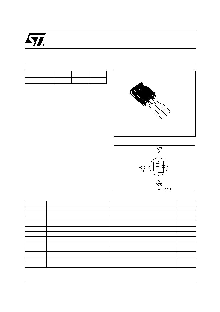
1
2
3
TO-247
ABSOLUTE MAXIMUM RATINGS
(
∑∑)
Pulse width limited by safe operating area.
(
∑)
Current limited by package
(1) I
SD
120A, di/dt
200A/µs, V
DD
V
(BR)DSS
, T
j
T
JMAX.
(2) Starting T
j
= 25
o
C, I
D
= 60 A, V
DD
= 15V
Symbol
Parameter
Value
Unit
V
DS
Drain-source Voltage (V
GS
= 0)
30
V
V
DGR
Drain-gate Voltage (R
GS
= 20 k
)
30
V
V
GS
Gate- source Voltage
± 20
V
I
D
(
∑)
Drain Current (continuous) at T
C
= 25∞C
120
A
I
D
Drain Current (continuous) at T
C
= 100∞C
120
A
I
DM
(
∑∑)
Drain Current (pulsed)
480
A
P
tot
Total Dissipation at T
C
= 25∞C
350
W
Derating Factor
2.33
W/∞C
dv/dt
(1)
Peak Diode Recovery voltage slope
1.5
V/ns
E
AS (2)
Single Pulse Avalanche Energy
4
J
T
stg
Storage Temperature
-55 to 175
∞C
T
j
Operating Junction Temperature
INTERNAL SCHEMATIC DIAGRAM
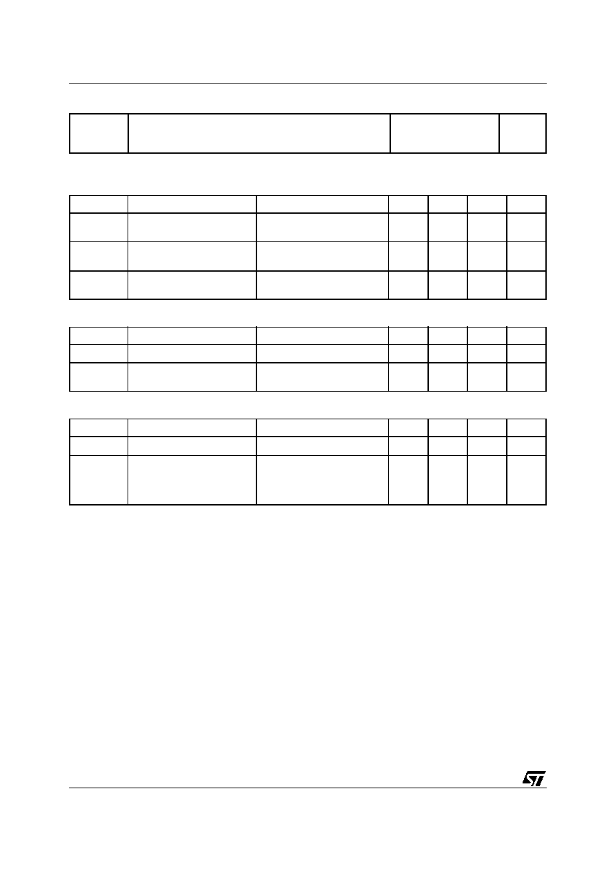
STW200NF03
2/8
THERMAL DATA
ELECTRICAL CHARACTERISTICS (T
case
= 25 ∞C unless otherwise specified)
OFF
ON
(1)
DYNAMIC
Rthj-case
Rthj-amb
T
l
Thermal Resistance Junction-case
Thermal Resistance Junction-ambient
Maximum Lead Temperature For Soldering Purpose
Max
Max
Typ
0.43
50
300
∞C/W
∞C/W
∞C
Symbol
Parameter
Test Conditions
Min.
Typ.
Max.
Unit
V
(BR)DSS
Drain-source Breakdown
Voltage
I
D
= 250 µA, V
GS
= 0
30
V
I
DSS
Zero Gate Voltage
Drain Current (V
GS
= 0)
V
DS
= Max Rating
V
DS
= Max Rating T
C
= 125∞C
1
10
µA
µA
I
GSS
Gate-body Leakage
Current (V
DS
= 0)
V
GS
= ± 20V
±100
nA
Symbol
Parameter
Test Conditions
Min.
Typ.
Max.
Unit
V
GS(th)
Gate Threshold Voltage
V
DS
= V
GS
I
D
= 250 µA
2
3
4
V
R
DS(on)
Static Drain-source On
Resistance
V
GS
= 10 V
I
D
= 60 A
0.002
0.0028
Symbol
Parameter
Test Conditions
Min.
Typ.
Max.
Unit
g
fs (*)
Forward Transconductance
V
DS
= 15 V
I
D
= 60 A
200
S
C
iss
C
oss
C
rss
Input Capacitance
Output Capacitance
Reverse Transfer
Capacitance
V
DS
= 25V, f = 1 MHz, V
GS
= 0
10
3.35
385
nF
nF
pF
3/8
STW200NF03
SWITCHING ON
SWITCHING OFF
SOURCE DRAIN DIODE
(*)
Pulsed: Pulse duration = 300 µs, duty cycle 1.5 %.
(
∑)
Pulse width limited by safe operating area.
Symbol
Parameter
Test Conditions
Min.
Typ.
Max.
Unit
t
d(on)
t
r
Turn-on Delay Time
Rise Time
V
DD
= 15 V
I
D
= 60 A
R
G
= 4.7
V
GS
= 10 V
(Resistive Load, Figure 3)
50
300
ns
ns
Q
g
Q
gs
Q
gd
Total Gate Charge
Gate-Source Charge
Gate-Drain Charge
V
DD
=15V I
D
=120A V
GS
= 10 V
(see test circuit, Figure 4)
210
63.5
63.5
280
nC
nC
nC
Symbol
Parameter
Test Conditions
Min.
Typ.
Max.
Unit
t
d(off)
t
f
Turn-off Delay Time
Fall Time
V
DD
= 15 V
I
D
= 60 A
R
G
= 4.7
,
V
GS
= 10 V
(Resistive Load, Figure 3)
100
80
ns
ns
Symbol
Parameter
Test Conditions
Min.
Typ.
Max.
Unit
I
SD
I
SDM
(
∑
)
Source-drain Current
Source-drain Current (pulsed)
120
480
A
A
V
SD
(*)
Forward On Voltage
I
SD
= 120 A
V
GS
= 0
1.3
V
t
rr
Q
rr
I
RRM
Reverse Recovery Time
Reverse Recovery Charge
Reverse Recovery Current
I
SD
= 120 A
di/dt = 100A/µs
V
DD
= 20 V
T
j
= 150∞C
(see test circuit, Figure 5)
90
250
5.5
ns
nC
A
ELECTRICAL CHARACTERISTICS (continued)
Thermal Impedance
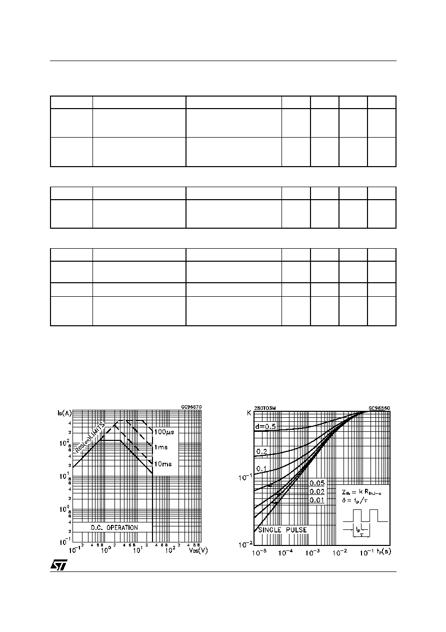
Safe Operating Area
STW200NF03
4/8
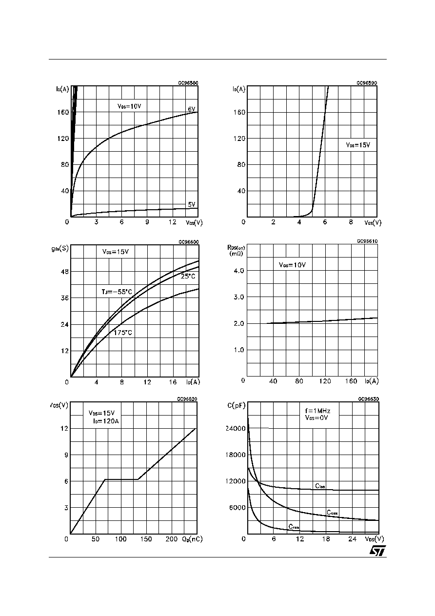
Output Characteristics
Transfer Characteristics
Transconductance
Static Drain-source On Resistance
Gate Charge vs Gate-source Voltage
Capacitance Variations
5/8
STW200NF03
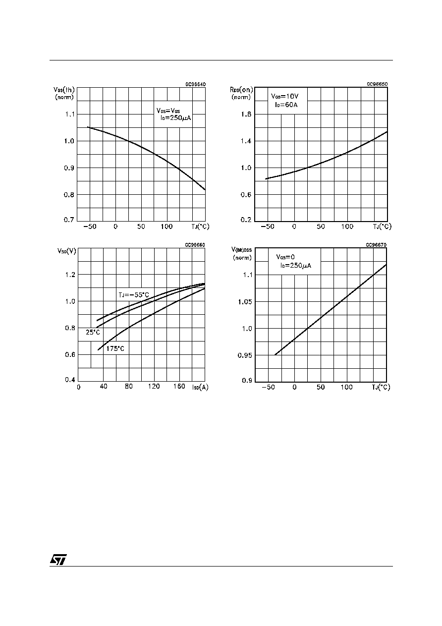
Normalized Gate Threshold Voltage vs Temperature
Normalized on Resistance vs Temperature
Source-drain Diode Forward Characteristics
Normalized Breakdown Voltage vs Temperature.
.
.
STW200NF03
6/8
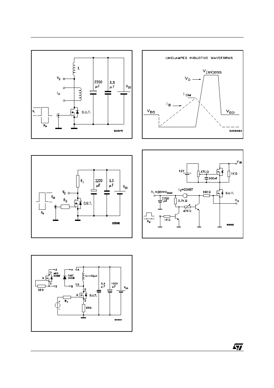
Fig. 1: Unclamped Inductive Load Test Circuit
Fig. 1: Unclamped Inductive Load Test Circuit
Fig. 2: Unclamped Inductive Waveform
Fig. 3: Switching Times Test Circuits For Resistive
Load
Fig. 4: Gate Charge test Circuit
Fig. 5: Test Circuit For Inductive Load Switching
And Diode Recovery Times
7/8
STW200NF03
DIM.
mm
inch
MIN.
TYP.
MAX.
MIN.
TYP.
MAX.
A
4.7
5.3
0.185
0.209
D
2.2
2.6
0.087
0.102
E
0.4
0.8
0.016
0.031
F
1
1.4
0.039
0.055
F3
2
2.4
0.079
0.094
F4
3
3.4
0.118
0.134
G
10.9
0.429
H
15.3
15.9
0.602
0.626
L
19.7
20.3
0.776
0.779
L3
14.2
14.8
0.559
0.582
L4
34.6
1.362
L5
5.5
0.217
M
2
3
0.079
0.118
P025P
TO-247 MECHANICAL DATA
STW200NF03
8/8
Information furnished is believed to be accurate and reliable. However, STMicroelectronics assumes no responsibility for the consequences
of use of such information nor for any infringement of patents or other rights of third parties which may result from its use. No license is granted
by implication or otherwise under any patent or patent rights of STMicroelectronics. Specifications mentioned in this publication are subject
to change without notice. This publication supersedes and replaces all information previously supplied. STMicroelectronics products are not
authorized for use as critical components in life support devices or systems without express written approval of STMicroelectronics.
The ST logo is registered trademark of STMicroelectronics
Æ
2002 STMicroelectronics - All Rights Reserved
All other names are the property of their respective owners.
STMicroelectronics GROUP OF COMPANIES
Australia - Brazil - Canada - China - Finland - France - Germany - Hong Kong - India - Israel - Italy - Japan - Malaysia - Malta - Morocco -
Singapore - Spain - Sweden - Switzerland - United Kingdom - United States.
http://www.st.com