PRELIMINARY DATA
This is preliminary information on a new product now in development or undergoing evaluation. Details are subject to
change without notice.
Rev 1
December 2005
1/27
2
STw4141
Single Coil Dual Output Step Down DC/DC Converter
for Digital Base Band and Multimedia Processor Supply
Features
Single coil dual output switching converter for
digital core supply & digital I/Os supply
� Digital I/O supply:V
OUT1
@ 200 mA
� CPU CORE supply:V
OUT2
@ 400 mA
Wide range of fixed output voltage
configurations available
High efficiency synchronous step down
converter with up to 92 % for the entire device
Size and cost optimized application board
(7x8 mm, height 1.2mm) three capacitors and
only one inductor necessary for both outputs
2.7 V to 5.5 V battery input range
�100mV output voltage accuracy full range in
PWM (Including Line and Load Transients)
900 kHz fixed frequency PWM operation
PFM mode operation at light load current
PWM/PFM switch can be done automatically or
forced by setting external pins (AUTO and
MODE/SYNC)
MODE/SYNC input pin for external clock
synchronization from 600 kHz to 1.5 MHz
VSEL input pin for V
OUT2
/V
OUT2(red.)
selection
Ultra low shutdown current (Iq<1 �A)
Short circuit and thermal shutdown protections
Applications
Mobile phones
PDAs and hand held terminals
Portable media players
Digital still camera
WLAN and Bluetooth applications
Description
The STw4141 is a single coil dual output
synchronous step down DC/DC converter that
requires only four standard external components.
It operates at a fixed 900 kHz switching frequency
in PWM mode. The device can operate in PFM
mode to maintain high efficiency over the full
range of output currents.
The STw4141 application requires a very small
PCB area and offers a very efficient, accurate,
space and cost saving solution to fulfill the
requirements of digital baseband or multimedia
processor supply (CORE & I/O).
Application Test Circuit
TFBGA 3x3mm
16 bumps 0.5 mm pitch
Solution size
7 x 8 mm
VOUT1
FB1
V
OUT1
=1.8V
C
OUT1
22 �F
6.3 V
VOUT2
FB2
V
OUT2
=1.0V/1.2V
C
OUT2
22 �F
6.3 V
PVDD
V
IN
=2.7V to 5.5V
C
IN
10 �F
6.3 V
PGND
VDD
EN
VLX1
VLX2
GND
MODE/SYNC
T_MODE
AUTO
L 4.7 �H
STw4141
VSEL
STATE
B1
D3
D4
C2
C3
C1
A4
D1
B4
D2
B2
A2
A3
A1
B3
C4
VOUT1
FB1
V
OUT1
=1.8V
C
OUT1
22 �F
6.3 V
VOUT2
FB2
V
OUT2
=1.0V/1.2V
C
OUT2
22 �F
6.3 V
PVDD
V
IN
=2.7V to 5.5V
C
IN
10 �F
6.3 V
PGND
VDD
EN
VLX1
VLX2
GND
MODE/SYNC
T_MODE
AUTO
L 4.7 �H
STw4141
VSEL
STATE
B1
D3
D4
C2
C3
C1
A4
D1
B4
D2
B2
A2
A3
A1
B3
C4
www.st.com

STw4141
3/27
Contents
1
STw4141 Pinout . . . . . . . . . . . . . . . . . . . . . . . . . . . . . . . . . . . . . . . . . . . . . . 5
2
Electrical Characteristics . . . . . . . . . . . . . . . . . . . . . . . . . . . . . . . . . . . . . . . 7
2.1
Absolute maximum ratings . . . . . . . . . . . . . . . . . . . . . . . . . . . . . . . . . . . . . . . 7
2.2
Thermal data . . . . . . . . . . . . . . . . . . . . . . . . . . . . . . . . . . . . . . . . . . . . . . . . . . 7
2.3
DC electrical characteristics . . . . . . . . . . . . . . . . . . . . . . . . . . . . . . . . . . . . . . 8
2.4
Dynamic electrical characteristics . . . . . . . . . . . . . . . . . . . . . . . . . . . . . . . . . . 9
2.5
Soft start . . . . . . . . . . . . . . . . . . . . . . . . . . . . . . . . . . . . . . . . . . . . . . . . . . . . 10
2.6
Settling time of VOUT2 . . . . . . . . . . . . . . . . . . . . . . . . . . . . . . . . . . . . . . . . . 10
2.7
Line transients . . . . . . . . . . . . . . . . . . . . . . . . . . . . . . . . . . . . . . . . . . . . . . . . 11
2.8
Load transients in AUTO mode . . . . . . . . . . . . . . . . . . . . . . . . . . . . . . . . . . . 11
2.9
Load transients in PWM mode . . . . . . . . . . . . . . . . . . . . . . . . . . . . . . . . . . . 12
2.10
Switching between PFM and PWM in FORCED MODE . . . . . . . . . . . . . . . . 13
2.11
Efficiency in PWM . . . . . . . . . . . . . . . . . . . . . . . . . . . . . . . . . . . . . . . . . . . . . 14
2.12
Efficiency in AUTO . . . . . . . . . . . . . . . . . . . . . . . . . . . . . . . . . . . . . . . . . . . . 15
2.13
Output voltages versus output currents in PWM and PFM . . . . . . . . . . . . . . 16
3
Functional Description . . . . . . . . . . . . . . . . . . . . . . . . . . . . . . . . . . . . . . . . 17
3.1
Introduction . . . . . . . . . . . . . . . . . . . . . . . . . . . . . . . . . . . . . . . . . . . . . . . . . . 17
3.2
PWM and PFM mode operation . . . . . . . . . . . . . . . . . . . . . . . . . . . . . . . . . . 17
3.3
Current limiter . . . . . . . . . . . . . . . . . . . . . . . . . . . . . . . . . . . . . . . . . . . . . . . . 17
3.4
Short circuit protection . . . . . . . . . . . . . . . . . . . . . . . . . . . . . . . . . . . . . . . . . 17
3.5
Thermal shutdown protection . . . . . . . . . . . . . . . . . . . . . . . . . . . . . . . . . . . . 18
4
Application information . . . . . . . . . . . . . . . . . . . . . . . . . . . . . . . . . . . . . . . 18
4.1
User mode details . . . . . . . . . . . . . . . . . . . . . . . . . . . . . . . . . . . . . . . . . . . . . 18
4.2
Automatic PWM/PFM mode . . . . . . . . . . . . . . . . . . . . . . . . . . . . . . . . . . . . . 19
4.3
User selected PWM/PFM mode . . . . . . . . . . . . . . . . . . . . . . . . . . . . . . . . . . 19
4.4
External clock synchronization . . . . . . . . . . . . . . . . . . . . . . . . . . . . . . . . . . . 20
4.5
Checking Transient response versus external components . . . . . . . . . . . . . 20
4.6
Bill of Material . . . . . . . . . . . . . . . . . . . . . . . . . . . . . . . . . . . . . . . . . . . . . . . . 20
4.6.1
Inductor selection . . . . . . . . . . . . . . . . . . . . . . . . . . . . . . . . . . . . . . . . . . . . . 20

STw4141
4/27
4.6.2
Input capacitor (CIN selection) . . . . . . . . . . . . . . . . . . . . . . . . . . . . . . . . . . . 21
4.6.3
Output capacitors (COUT selection) . . . . . . . . . . . . . . . . . . . . . . . . . . . . . . . 21
4.6.4
Capacitors selection . . . . . . . . . . . . . . . . . . . . . . . . . . . . . . . . . . . . . . . . . . . 21
4.7
PCB layout considerations . . . . . . . . . . . . . . . . . . . . . . . . . . . . . . . . . . . . . . 21
4.7.1
PCB layout . . . . . . . . . . . . . . . . . . . . . . . . . . . . . . . . . . . . . . . . . . . . . . . . . . . 22
4.7.2
TFBGA16 internal bumps access . . . . . . . . . . . . . . . . . . . . . . . . . . . . . . . . . 23
5
Package Outline and Mechanical Data . . . . . . . . . . . . . . . . . . . . . . . . . . . 24
6
Revision history . . . . . . . . . . . . . . . . . . . . . . . . . . . . . . . . . . . . . . . . . . . . . . 26
STw4141
1 STw4141 Pinout
5/27
1 STw4141
Pinout
Figure 1.
Pin assignment in TFBGA 3x3 mm - 16 bumps 0.5 mm pitch
Table 2.
STw4141 pin description
Pin
Symbol
Description
A1
PGND
Power ground
B1
PVDD
Power supply voltage
C1
MODE/SYNC
MODE/SYNC = High to forced PWM mode
MODE/SYNC = Low to forced PFM mode
MODE/SYNC = 600 kHz - 1.5 MHz external clock synchronization in PWM
D1
FB1
Feedback 1
A2
VLX1
External inductor connection pin 1
B2
STATE
Output STATE pin allow the user to monitor operation mode of the product
STATE = High - PFM mode
STATE = Low - PWM mode
If not used must be left unconnected.
C2
AUTO
PWM/PFM automatic switch control pin
AUTO = High - PWM/PFM mode automatic switch ENABLED
AUTO = Low - PWM/PFM mode automatic switch DISABLED
PWM/PFM mode controlled by MODE/SYNC pin)
D2
FB2
Feedback 2
A3
VLX2
External inductor connection pin 2
B3
T_MODE
Input signal for test mode selection. This pin must be connected to GND.
C3
VSEL
Voltage selection input
VSEL = High - VOUT1 = 1.8V, VOUT2 = 1.2V (valid for STA1)
VSEL = Low - VOUT1 = 1.8V, VOUT2 = 1.0V (valid for STA1)
(For other voltage options see
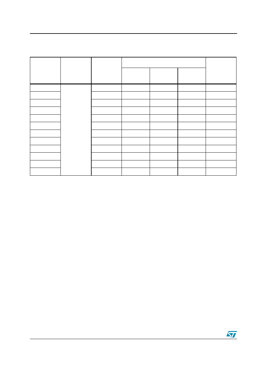
Table 1: STw4141 ordering information
)
D3
VDD
Signal supply voltage
A4
VOUT1
Output voltage 1
PGND
PVDD
MODE/
SYNC
FB1
VLX1
STATE
AUTO
FB2
VLX2
VSEL
VDD
VOUT1
VOUT2
GND
EN
A
B
C
D
1
2
3
4
T_MODE
PGND
PVDD
MODE/
SYNC
FB1
VLX1
STATE
AUTO
FB2
VLX2
VSEL
VDD
VOUT1
VOUT2
GND
EN
1
2
3
4
A
B
C
D
T_MODE
Top view
Bottom view
1
2
3
4
A
B
C
D
A
B
C
D
4
3
2
1