 | –≠–ª–µ–∫—Ç—Ä–æ–Ω–Ω—ã–π –∫–æ–º–ø–æ–Ω–µ–Ω—Ç: STW47NM60 | –°–∫–∞—á–∞—Ç—å:  PDF PDF  ZIP ZIP |
1/6
ADVANCED DATA
January 2003
STW47NM60
N-CHANNEL 600V - 0.075
- 47A TO-247
MDmeshTMPower MOSFET
(1) I
SD
47A, di/dt
400A/µs, V
DD
V
(BR)DSS
, T
j
T
JMAX.
TYPICAL R
DS
(on) = 0.075
HIGH dv/dt AND AVALANCHE CAPABILITIES
100% AVALANCHE TESTED
LOW INPUT CAPACITANCE AND GATE
CHARGE
LOW GATE INPUT RESISTANCE
TIGHT PROCESS CONTROL AND HIGH
MANUFACTURING YIELDS
DESCRIPTION
This improved version of MDmeshTM which is based
on Multiple Drain process represents the new
benchmark in high voltage MOSFETs. The resulting
product exhibits even lower on-resistance, impres-
sively high dv/dt and excellent avalanche character-
istics. The adoption of the Company's proprietary
strip technique yields overall performances that are
significantly better than that of similar competition's
products.
APPLICATIONS
The MDmeshTM family is very suitable for increasing
power density of high voltage converters allowing
system miniaturization and higher efficiencies.
ABSOLUTE MAXIMUM RATINGS
(∑)Pulse width limited by safe operating area
TYPE
V
DSS
R
DS(on)
R
ds(on)
*Q
g
I
D
STW47NM60
600V
< 0.09
7.2
*nC
47 A
Symbol
Parameter
Value
Unit
V
DS
Drain-source Voltage (V
GS
= 0)
600
V
V
DGR
Drain-gate Voltage (R
GS
= 20 k
)
600
V
V
GS
Gate- source Voltage
±30
V
I
D
Drain Current (continuous) at T
C
= 25∞C
47
A
I
D
Drain Current (continuous) at T
C
= 100∞C
28
A
I
DM
( )
Drain Current (pulsed)
180
A
P
TOT
Total Dissipation at T
C
= 25∞C
417
W
Derating Factor
3.33
W/∞C
dv/dt (1)
Peak Diode Recovery voltage slope
15
V/ns
T
stg
Storage Temperature
≠65 to 150
∞C
T
j
Max. Operating Junction Temperature
150
∞C
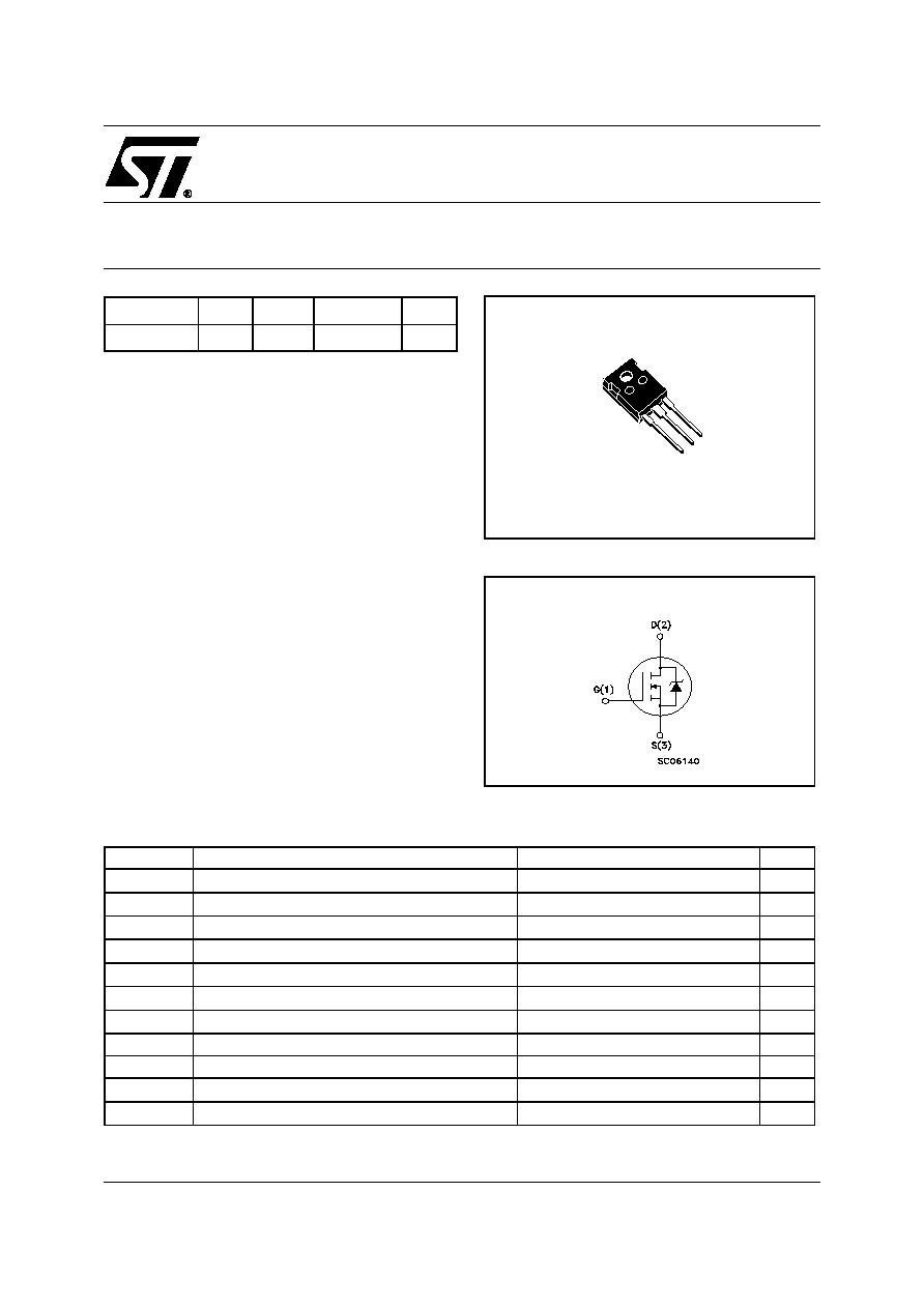
1
2
3
TO-247
INTERNAL SCHEMATIC DIAGRAM
STW47NM60
2/6
THERMAL DATA
AVALANCHE CHARACTERISTICS
ELECTRICAL CHARACTERISTICS (T
CASE
= 25 ∞C UNLESS OTHERWISE SPECIFIED)
OFF
ON (1)
DYNAMIC
1. Pulsed: Pulse duration = 300 µs, duty cycle 1.5 %.
2. C
oss eq.
is defined as a constant equivalent capacitance giving the same charging time as C
oss
when V
DS
increases from 0 to 80%
V
DSS
Rthj-case
Thermal Resistance Junction-case
Max
0.3
∞C/W
Rthj-amb
Thermal Resistance Junction-ambient
Max
30
∞C/W
T
l
Maximum Lead Temperature For Soldering Purpose
300
∞C
Symbol
Parameter
Max Value
Unit
I
AR
Avalanche Current, Repetitive or Not-Repetitive
(pulse width limited by T
j
max)
15
A
E
AS
Single Pulse Avalanche Energy
(starting T
j
= 25 ∞C, I
D
= I
AR
, V
DD
= 35 V)
850
mJ
Symbol
Parameter
Test Conditions
Min.
Typ.
Max.
Unit
V
(BR)DSS
Drain-source
Breakdown Voltage
I
D
= 250 µA, V
GS
= 0
600
V
I
DSS
Zero Gate Voltage
Drain Current (V
GS
= 0)
V
DS
= Max Rating
10
µA
V
DS
= Max Rating, T
C
= 125 ∞C
100
µA
I
GSS
Gate-body Leakage
Current (V
DS
= 0)
V
GS
= ±30 V
±100
nA
Symbol
Parameter
Test Conditions
Min.
Typ.
Max.
Unit
V
GS(th)
Gate Threshold Voltage
V
DS
= V
GS
, I
D
= 250 µA
3
4
5
V
R
DS(on)
Static Drain-source On
Resistance
V
GS
= 10 V, I
D
= 23.5 A
0.075
0.09
Symbol
Parameter
Test Conditions
Min.
Typ.
Max.
Unit
g
fs
(1)
Forward Transconductance
V
DS
> I
D(on)
x R
DS(on)max,
I
D
= 23.5 A
15
S
C
iss
Input Capacitance
V
DS
= 25 V, f = 1 MHz, V
GS
= 0
3800
pF
C
oss
Output Capacitance
1250
pF
C
rss
Reverse Transfer
Capacitance
46
pF
C
oss eq.
(2)
Equivalent Output
Capacitance
V
GS
= 0 V, V
DS
= 0 V to 480 V
340
pF
R
G
Gate Input Resistance
f=1 MHz Gate DC Bias = 0
Test Signal Level = 20 mV
Open Drain
1.4
3/6
STW47NM60
ELECTRICAL CHARACTERISTICS (CONTINUED)
SWITCHING ON
SWITCHING OFF
SOURCE DRAIN DIODE
Note: 1. Pulsed: Pulse duration = 300 µs, duty cycle 1.5 %.
2. Pulse width limited by safe operating area.
Symbol
Parameter
Test Conditions
Min.
Typ.
Max.
Unit
t
d(on)
Turn-on Delay Time
V
DD
= 250 V, I
D
= 23.5 A
R
G
= 4.7
V
GS
= 10 V
(see test circuit, Figure 3)
30
ns
t
r
Rise Time
20
ns
Q
g
Total Gate Charge
V
DD
= 400 V, I
D
= 47 A,
V
GS
= 10 V
96
134
nC
Q
gs
Gate-Source Charge
31
nC
Q
gd
Gate-Drain Charge
43
nC
Symbol
Parameter
Test Conditions
Min.
Typ.
Max.
Unit
t
r(Voff)
Off-voltage Rise Time
V
DD
= 400 V, I
D
= 47 A,
R
G
= 4.7
,
V
GS
= 10 V
(see test circuit, Figure 5)
16
ns
t
f
Fall Time
23
ns
t
c
Cross-over Time
40
ns
Symbol
Parameter
Test Conditions
Min.
Typ.
Max.
Unit
I
SD
Source-drain Current
47
A
I
SDM
(2)
Source-drain Current (pulsed)
180
A
V
SD
(1)
Forward On Voltage
I
SD
= 47 A, V
GS
= 0
1.5
V
t
rr
Q
rr
I
RRM
Reverse Recovery Time
Reverse Recovery Charge
Reverse Recovery Current
I
SD
= 47 A, di/dt = 100 A/µs,
V
DD
= 100 V, T
j
= 25∞C
(see test circuit, Figure 5)
508
10
40
ns
µC
A
t
rr
Q
rr
I
RRM
Reverse Recovery Time
Reverse Recovery Charge
Reverse Recovery Current
I
SD
= 47 A, di/dt = 100 A/µs,
V
DD
= 100 V, T
j
= 150∞C
(see test circuit, Figure 5)
650
14
43
ns
µC
A
STW47NM60
4/6
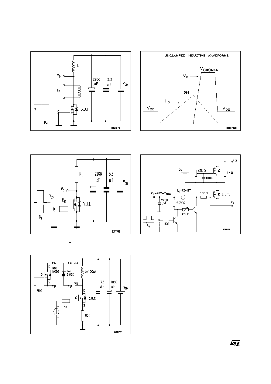
Fig. 5: Test Circuit For Inductive Load Switching
And Diode Recovery Times
Fig. 4: Gate Charge test Circuit
Fig. 2: Unclamped Inductive Waveform
Fig. 1: Unclamped Inductive Load Test Circuit
Fig. 3: Switching Times Test Circuit For
Resistive Load
5/6
STW47NM60
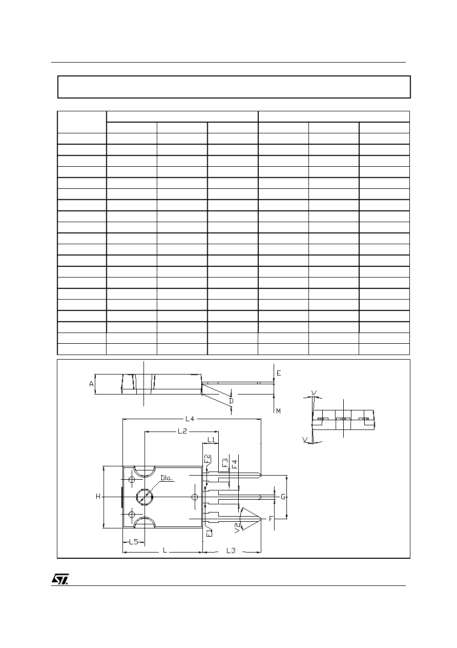
DIM.
mm.
inch
MIN.
TYP
MAX.
MIN.
TYP.
MAX.
A
4.85
5.15
0.19
0.20
D
2.20
2.60
0.08
0.10
E
0.40
0.80
0.015
0.03
F
1
1.40
0.04
0.05
F1
3
0.11
F2
2
0.07
F3
2
2.40
0.07
0.09
F4
3
3.40
0.11
0.13
G
10.90
0.43
H
15.45
15.75
0.60
0.62
L
19.85
20.15
0.78
0.79
L1
3.70
4.30
0.14
0.17
L2
18.50
0.72
L3
14.20
14.80
0.56
0.58
L4
34.60
1.36
L5
5.50
0.21
M
2
3
0.07
0.11
V
5∫
5∫
V2
60∫
60∫
Dia
3.55
3.65
0.14
0.143
TO-247 MECHANICAL DATA