 | –≠–ª–µ–∫—Ç—Ä–æ–Ω–Ω—ã–π –∫–æ–º–ø–æ–Ω–µ–Ω—Ç: STW7NA90 | –°–∫–∞—á–∞—Ç—å:  PDF PDF  ZIP ZIP |
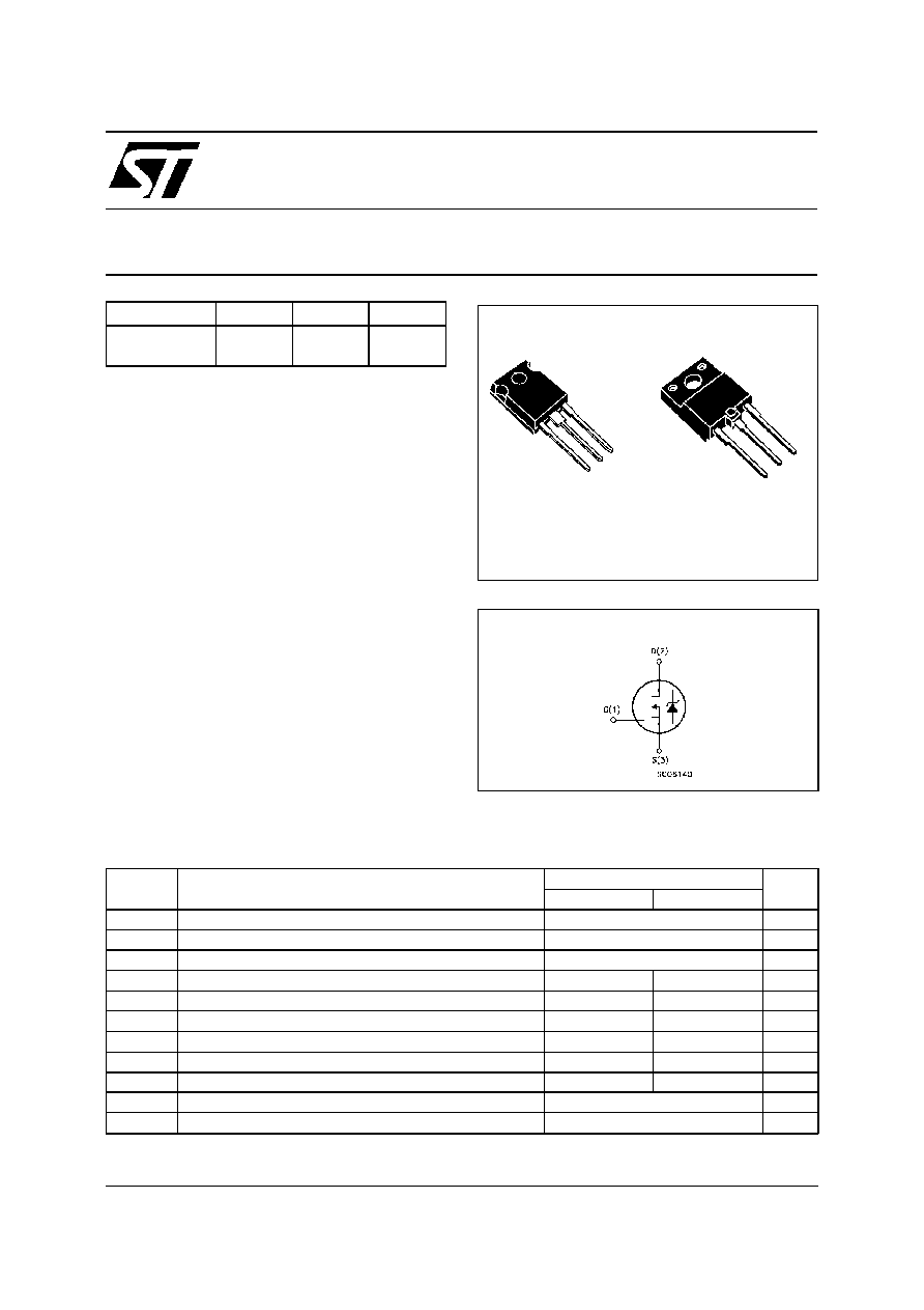
STW7NA90
STH7NA90FI
N - CHANNEL 900V - 1.05
- 7A - TO-247/ISOWATT218
FAST POWER MOSFET
s
TYPICAL R
DS(on)
= 1.05
s
±
30V GATE TO SOURCE VOLTAGE RATING
s
100% AVALANCHE TESTED
s
REPETITIVE AVALANCHE DATA AT 100
o
C
s
LOW INTRINSIC CAPACITANCE
s
GATE CHARGE MINIMIZED
s
REDUCED VOLTAGE SPREAD
APPLICATIONS
s
HIGH CURRENT, HIGH SPEED SWITCHING
s
SWITCH MODE POWER SUPPLY (SMPS)
s
CONSUMER AND INDUSTRIAL LIGHTING
s
DC-AC CONVERTER FOR WELDING
EQUIPMENT AND UNINTERRUPTABLE
POWER SUPPLY (UPS)
Æ
INTERNAL SCHEMATIC DIAGRAM
ABSOLUTE MAXIMUM RATINGS
Symbol
Parameter
Value
Un it
ST W7NA90
STH7NA90F I
V
DS
Drain-source Voltage (V
GS
= 0)
900
V
V
DGR
Drain- gate Voltage (R
GS
= 20 k
)
900
V
V
GS
G ate-source Volt age
±
30
V
I
D
Drain Current (continuous) at T
c
= 25
o
C
7
4.7
A
I
D
Drain Current (continuous) at T
c
= 100
o
C
4
3
A
I
DM
(
∑
)
Drain Current (pulsed)
30
30
A
P
tot
T otal Dissipat ion at T
c
= 25
o
C
190
70
W
Derating Factor
1.52
0.56
W /
o
C
V
ISO
I nsulation W ithstand Voltage (DC)
------
4000
V
T
s tg
Storage Temperature
-65 to 150
o
C
T
j
Max. Operating Junction Temperature
150
o
C
(
∑
) Pulse width limited by safe operating area
TYPE
V
DSS
R
DS(on)
I
D
STW 7NA90
STH7NA90F I
900 V
900 V
< 1.3
<
1.3
7 A
4. 7 A
October 1998
1
2
3
TO-247
ISOWATT218
1
2
3
1/9
THERMAL DATA
TO-247
ISOWATT 218
R
thj -case
Thermal Resistance Junction-case
Max
0. 65
1. 78
o
C/W
R
thj -amb
R
thc-sink
T
l
Thermal Resistance Junction-ambient
Max
Thermal Resistance Case-sink
Typ
Maximum Lead Temperature F or Soldering Purpose
30
0.1
300
o
C/W
o
C/W
o
C
AVALANCHE CHARACTERISTICS
Symbo l
Parameter
Max Value
Unit
I
AR
Avalanche Current, Repetitive or Not-Repetitive
(pulse width limited by T
j
max)
7
A
E
AS
Single Pulse Avalanche Energy
(starting T
j
= 25
o
C, I
D
= I
AR
, V
DD
= 25 V)
700
mJ
ELECTRICAL CHARACTERISTICS (T
case
= 25
o
C unless otherwise specified)
OFF
Symbo l
Parameter
Test Con ditions
Min.
Typ.
Max.
Unit
V
(BR)DSS
Drain-source
Breakdown Voltage
I
D
= 250
µ
A
V
GS
= 0
900
V
I
DSS
Zero Gat e Voltage
Drain Current (V
GS
= 0)
V
DS
= Max Rat ing
V
DS
= Max Rat ing
T
c
= 100
o
C
50
500
µ
A
µ
A
I
G SS
Gat e-body Leakage
Current (V
DS
= 0)
V
GS
=
±
30 V
±
100
nA
ON (
)
Symbo l
Parameter
Test Con ditions
Min.
Typ.
Max.
Unit
V
G S(th)
Gat e Threshold Voltage V
DS
= V
GS
I
D
= 250
µ
A
2.25
3
3.75
V
R
DS(on)
Static Drain-source On
Resistance
V
GS
= 10 V
I
D
= 3.5 A
1.05
1. 3
I
D(o n)
On State Drain Current
V
DS
> I
D(o n)
x R
DS(on )ma x
V
GS
= 10 V
7
A
DYNAMIC
Symbo l
Parameter
Test Con ditions
Min.
Typ.
Max.
Unit
g
f s
(
)
Forward
Transconductance
V
DS
> I
D(o n)
x R
DS(on )ma x
I
D
= 3.5 A
7
9
S
C
iss
C
os s
C
rss
Input Capacitance
Out put Capacitance
Reverse Transfer
Capacitance
V
DS
= 25 V
f = 1 MHz
V
GS
= 0
3100
310
80
4000
380
105
pF
pF
pF
STW7NA90 - STH7NA90FI
2/9
ELECTRICAL CHARACTERISTICS (continued)
SWITCHING ON
Symbo l
Parameter
Test Con ditions
Min.
Typ.
Max.
Unit
t
d(on)
t
r
Turn-on Time
Rise Time
V
DD
= 450 V
I
D
= 3.5 A
R
G
= 4.7
V
G S
= 10 V
(see t est circuit, f igure 3)
40
41
54
63
ns
ns
Q
g
Q
gs
Q
gd
Tot al G ate Charge
Gat e-Source Charge
Gat e-Drain Charge
V
DD
= 720 V
I
D
= 7 A
V
G S
= 10 V
120
20
60
170
nC
nC
nC
SWITCHING OFF
Symbo l
Parameter
Test Con ditions
Min.
Typ.
Max.
Unit
t
r (Voff)
t
f
t
c
Off -volt age Rise T ime
Fall T ime
Cross-over Time
V
DD
= 720 V
I
D
= 7 A
R
G
= 4.7
V
G S
= 10 V
(see t est circuit, f igure 5)
50
18
73
65
23
97
ns
ns
ns
SOURCE DRAIN DIODE
Symbo l
Parameter
Test Con ditions
Min.
Typ.
Max.
Unit
I
SD
I
SDM
(
∑
)
Source-drain Current
Source-drain Current
(pulsed)
7
30
A
A
V
SD
(
)
Forward On Voltage
I
SD
= 7 A
V
GS
= 0
1. 6
V
t
rr
Q
rr
I
RRM
Reverse Recovery
Time
Reverse Recovery
Charge
Reverse Recovery
Current
I
SD
= 7 A
di/ dt = 100 A/
µ
s
V
DD
= 100 V
T
j
= 150
o
C
(see t est circuit, f igure 5)
830
13.8
33
ns
µ
C
A
(
) Pulsed: Pulse duration = 300
µ
s, duty cycle 1.5 %
(
∑
) Pulse width limited by safe operating area
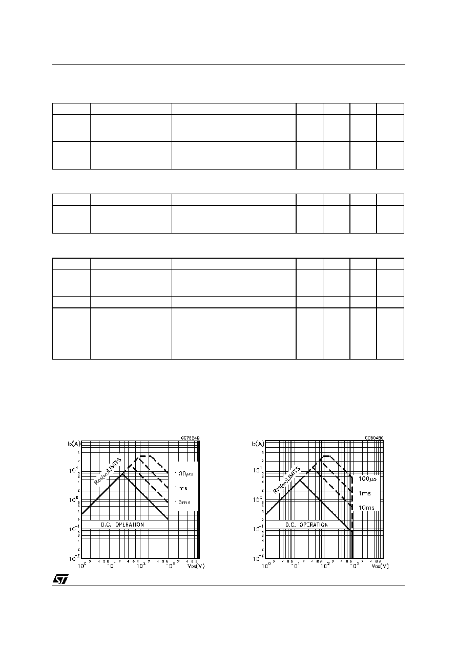
Safe Operating Area for TO-247
Safe Operating Area for ISOWATT218
STW7NA90 - STH7NA90FI
3/9
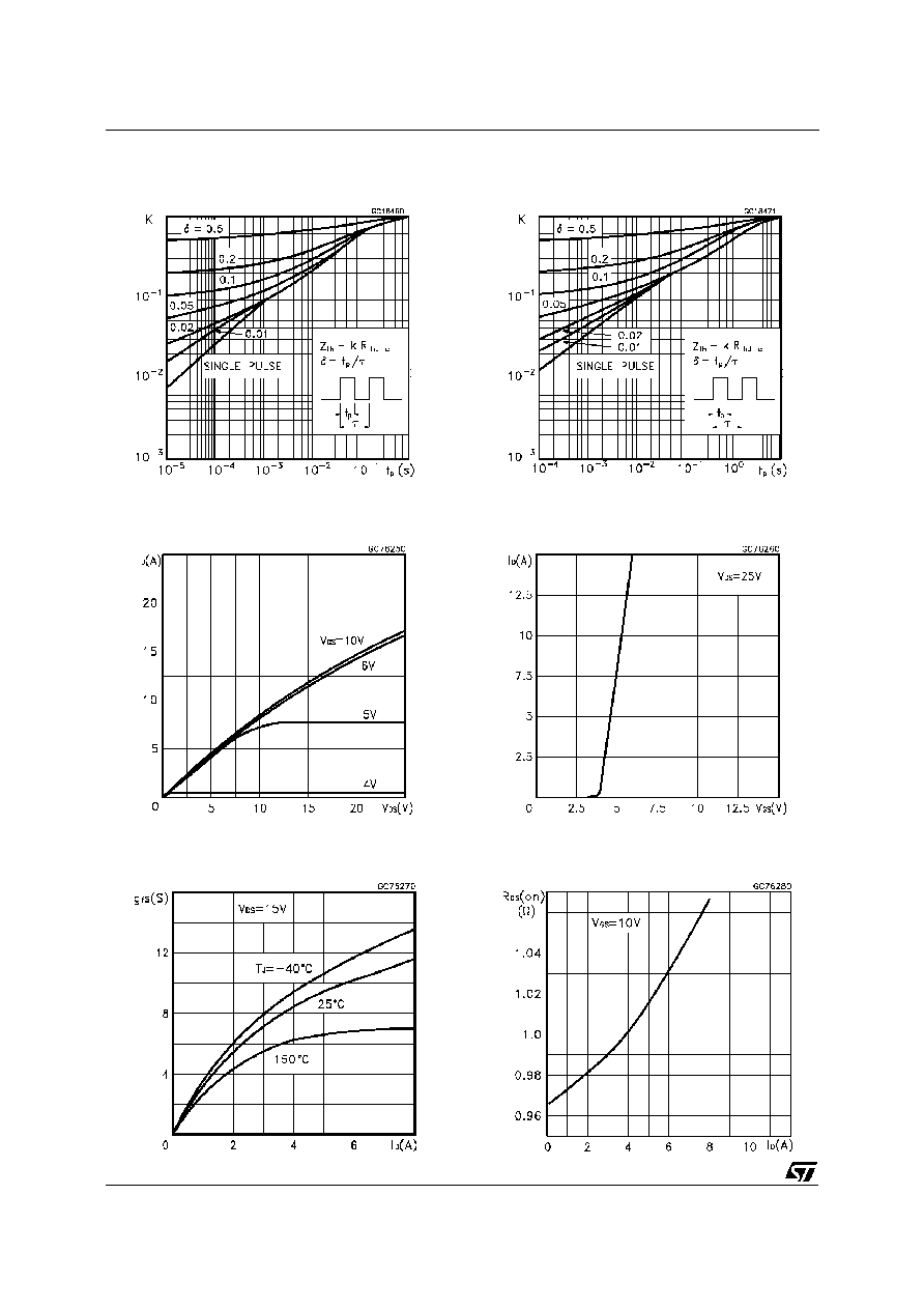
Thermal Impedance for TO-247
Output Characteristics
Transconductance
Thermal Impedance for ISOWATT218
Transfer Characteristics
Static Drain-source On Resistance
STW7NA90 - STH7NA90FI
4/9
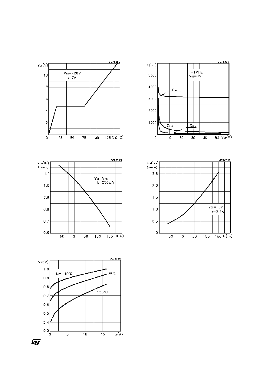
Gate Charge vs Gate-source Voltage
Normalized Gate Threshold Voltage vs
Temperature
Source-drain Diode Forward Characteristics
Capacitance Variations
Normalized On Resistance vs Temperature
STW7NA90 - STH7NA90FI
5/9
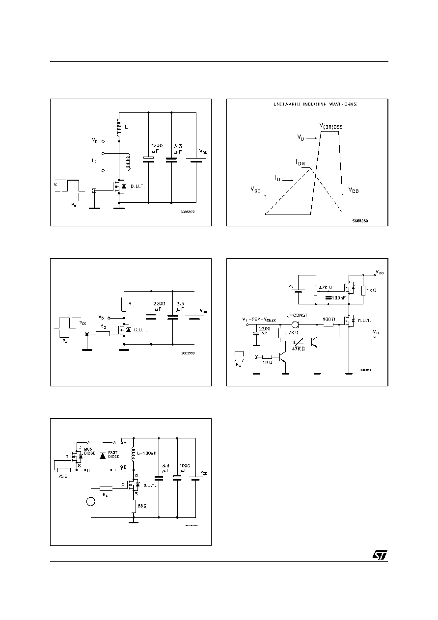
Fig. 1: Unclamped Inductive Load Test Circuit
Fig. 3: Switching Times Test Circuits For
Resistive Load
Fig. 2: Unclamped Inductive Waveform
Fig. 4: Gate Charge test Circuit
Fig. 5: Test Circuit For Inductive Load Switching
And Diode Recovery Times
STW7NA90 - STH7NA90FI
6/9
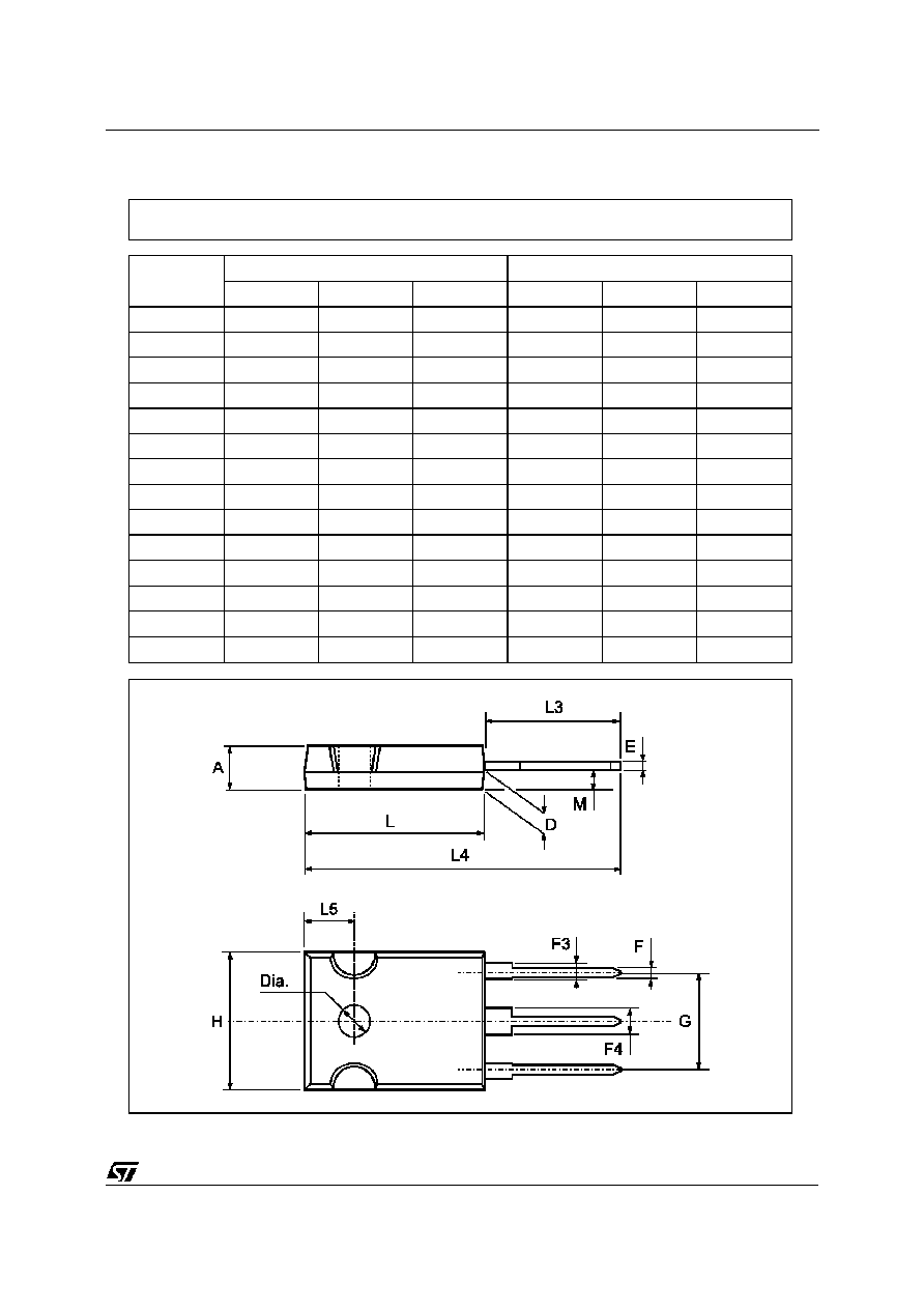
DIM.
mm
inch
MIN.
TYP.
MAX.
MIN.
TYP.
MAX.
A
4.7
5.3
0.185
0.209
D
2.2
2.6
0.087
0.102
E
0.4
0.8
0.016
0.031
F
1
1.4
0.039
0.055
F3
2
2.4
0.079
0.094
F4
3
3.4
0.118
0.134
G
10.9
0.429
H
15.3
15.9
0.602
0.626
L
19.7
20.3
0.776
0.779
L3
14.2
14.8
0.559
0.413
0.582
L4
34.6
1.362
L5
5.5
0.217
M
2
3
0.079
0.118
Dia
3.55
3.65
0.140
0.144
P025P
TO-247 MECHANICAL DATA
STW7NA90 - STH7NA90FI
7/9
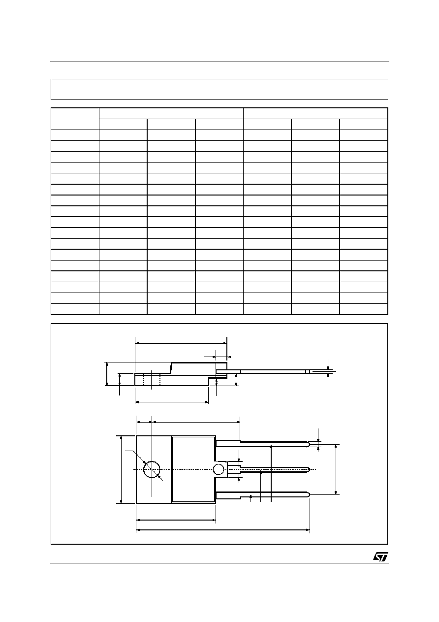
DIM.
mm
inch
MIN.
TYP.
MAX.
MIN.
TYP.
MAX.
A
5.35
5.65
0.210
0.222
C
3.3
3.8
0.130
0.149
D
2.9
3.1
0.114
0.122
D1
1.88
2.08
0.074
0.081
E
0.75
1
0.029
0.039
F
1.05
1.25
0.041
0.049
G
10.8
11.2
0.425
0.441
H
15.8
16.2
0.622
0.637
L1
20.8
21.2
0.818
0.834
L2
19.1
19.9
0.752
0.783
L3
22.8
23.6
0.897
0.929
L4
40.5
42.5
1.594
1.673
L5
4.85
5.25
0.190
0.206
L6
20.25
20.75
0.797
0.817
M
3.5
3.7
0.137
0.145
N
2.1
2.3
0.082
0.090
U
4.6
0.181
L1
A
C
D
E
H
G
M
F
L6
1
2
3
U
L5
L4
D1
N
L3
L2
P025C
ISOWATT218 MECHANICAL DATA
STW7NA90 - STH7NA90FI
8/9

Information furnished is believed to be accurate and reliable. However, STMicroelectronics assumes no responsibility for the consequences
of use of such information nor for any infringement of patents or other rights of third parties which may result from its use. No license is
granted by implication or otherwise under any patent or patent rights of STMicroelectronics. Specification mentioned in this publication are
subject to change without notice. This publication supersedes and replaces all information previously supplied. STMicroelectronics products
are not authorized for use as critical components in life support devices or systems without express written approval of STMicroelectronics.
The ST logo is a trademark of STMicroelectronics
©
1998 STMicroelectronics ≠ Printed in Italy ≠ All Rights Reserved
STMicroelectronics GROUP OF COMPANIES
Australia - Brazil - Canada - China - France - Germany - Italy - Japan - Korea - Malaysia - Malta - Mexico - Morocco - The Netherlands -
Singapore - Spain - Sweden - Switzerland - Taiwan - Thailand - United Kingdom - U.S.A.
http://www.st.com
.
STW7NA90 - STH7NA90FI
9/9