1/8
September 2002
STW80NF55-08
N-CHANNEL 55V - 0.0065
- 80A TO-247
STripFETTM POWER MOSFET
(1) Starting T
j
= 25∞C, I
D
= 40A, V
DD
= 40V
(*) Current Limited by wire bonding
s
TYPICAL R
DS
(on) = 0.0065
s
EXCEPTIONAL dv/dt CAPABILITY
s
100% AVALANCHE TESTED
s
LOW THRESHOLD DRIVE
DESCRIPTION
This Power MOSFET is the latest development of
STMicroelectronics unique "Single Feature SizeTM"
strip-based process. The resulting transistor shows
extremely high packing density for low on-resis-
tance, rugged avalanche characteristics and less
critical alignment steps therefore a remarkable
manufacturing reproducibility.
APPLICATIONS
s
DC-AC & DC-DC CONVERTERS
s
HIGH CURRENT, HIGH SPEED SWITCHING
s
SOLENOID AND RELAY DRIVERS
s
MOTOR CONTROL, AUDIO AMPLIFIERS
ABSOLUTE MAXIMUM RATINGS
(
q
) Pulse width limited by safe operating area
TYPE
V
DSS
R
DS(on)
I
D
STW80NF55-08
55 V
< 0.008
80 A
Symbol
Parameter
Value
Unit
V
DS
Drain-source Voltage (V
GS
= 0)
55
V
V
DGR
Drain-gate Voltage (R
GS
= 20 k
)
55
V
V
GS
Gate- source Voltage
±20
V
I
D
(*)
Drain Current (continuous) at T
C
= 25∞C
80
A
I
D
Drain Current (continuous) at T
C
= 100∞C
80
A
I
DM
(
l
)
Drain Current (pulsed)
320
A
P
TOT
Total Dissipation at T
C
= 25∞C
300
W
Derating Factor
2
W/∞C
E
AS
(1)
Single Pulse Avalanche Energy
870
mJ
T
stg
Storage Temperature
≠65 to 175
∞C
T
j
Max. Operating Junction Temperature
175
∞C
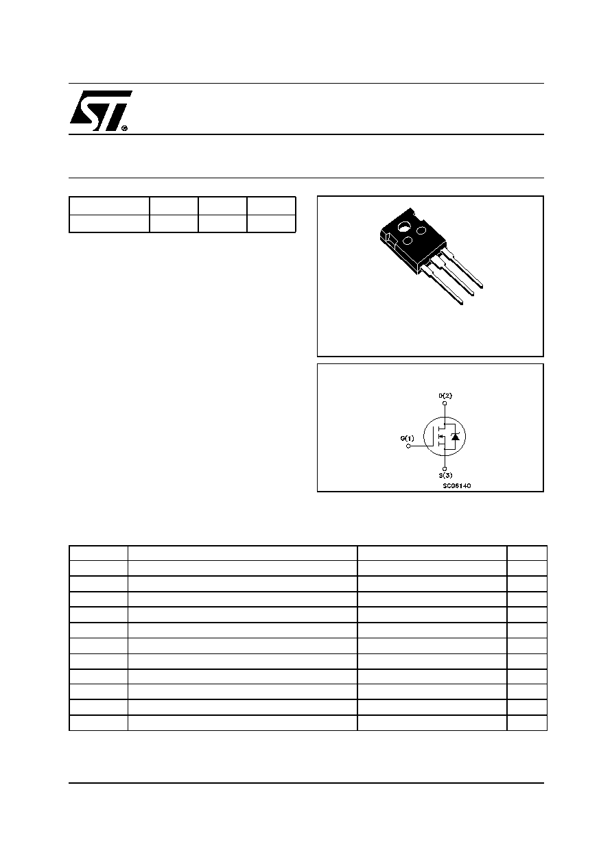
TO-247
1
2
3
INTERNAL SCHEMATIC DIAGRAM
STW80NF55-08
2/8
THERMAL DATA
ELECTRICAL CHARACTERISTICS (T
CASE
= 25 ∞C UNLESS OTHERWISE SPECIFIED)
OFF
ON
(1)
DYNAMIC
Rthj-case
Thermal Resistance Junction-case Max
0.5
∞C/W
Rthj-amb
Thermal Resistance Junction-ambient Max
62.5
∞C/W
T
l
Maximum Lead Temperature For Soldering Purpose
300
∞C
Symbol
Parameter
Test Conditions
Min.
Typ.
Max.
Unit
V
(BR)DSS
Drain-source
Breakdown Voltage
I
D
= 250 µA, V
GS
= 0
55
V
I
DSS
Zero Gate Voltage
Drain Current (V
GS
= 0)
V
DS
= Max Rating
1
µA
V
DS
= Max Rating, T
C
= 125 ∞C
10
µA
I
GSS
Gate-body Leakage
Current (V
DS
= 0)
V
GS
= ±20V
±100
nA
Symbol
Parameter
Test Conditions
Min.
Typ.
Max.
Unit
V
GS(th)
Gate Threshold Voltage
V
DS
= V
GS
, I
D
= 250µA
2
3
4
V
R
DS(on)
Static Drain-source On
Resistance
V
GS
= 10V, I
D
= 40 A
0.0065
0.008
Symbol
Parameter
Test Conditions
Min.
Typ.
Max.
Unit
g
fs
(1)
Forward Transconductance
V
DS
> 2.5 V
,
I
D
=18 A
20
S
C
iss
Input Capacitance
V
DS
= 25V, f = 1 MHz, V
GS
= 0
3850
pF
C
oss
Output Capacitance
800
pF
C
rss
Reverse Transfer
Capacitance
250
pF
3/8
STW80NF55-08
ELECTRICAL CHARACTERISTICS (CONTINUED)
SWITCHING ON
SWITCHING OFF
SOURCE DRAIN DIODE
Note: 1. Pulsed: Pulse duration = 300 µs, duty cycle 1.5 %.
2. Pulse width limited by safe operating area.
Symbol
Parameter
Test Conditions
Min.
Typ.
Max.
Unit
t
d(on)
Turn-on Delay Time
V
DD
= 27V, I
D
= 40A
R
G
= 4.7
V
GS
= 10V
(see test circuit, Figure 3)
25
ns
t
r
Rise Time
85
ns
Q
g
Q
gs
Q
gd
Total Gate Charge
Gate-Source Charge
Gate-Drain Charge
V
DD
= 80V, I
D
= 80A,
V
GS
= 10V
115
24
46
150
nC
nC
nC
Symbol
Parameter
Test Conditions
Min.
Typ.
Max.
Unit
t
d(off)
t
f
Turn-off-Delay Time
Fall Time
V
DD
= 27V, I
D
= 40A,
R
G
= 4.7
,
V
GS
= 10V
(see test circuit, Figure 3)
70
25
ns
ns
t
d(off)
t
f
t
c
Off-voltage Rise Time
Fall Time
Cross-over Time
Vclamp =44V, I
D
=80A
R
G
= 4.7
,
V
GS
= 10V
(see test circuit, Figure 5)
85
75
110
ns
ns
ns
Symbol
Parameter
Test Conditions
Min.
Typ.
Max.
Unit
I
SD
Source-drain Current
80
A
I
SDM
(1)
Source-drain Current (pulsed)
320
A
V
SD
(2)
Forward On Voltage
I
SD
= 80A, V
GS
= 0
1.5
V
t
rr
Q
rr
I
RRM
Reverse Recovery Time
Reverse Recovery Charge
Reverse Recovery Current
I
SD
= 80A, di/dt = 100A/µs,
V
DD
= 50V, T
j
= 150∞C
(see test circuit, Figure 5)
80
250
6.4
ns
nC
A
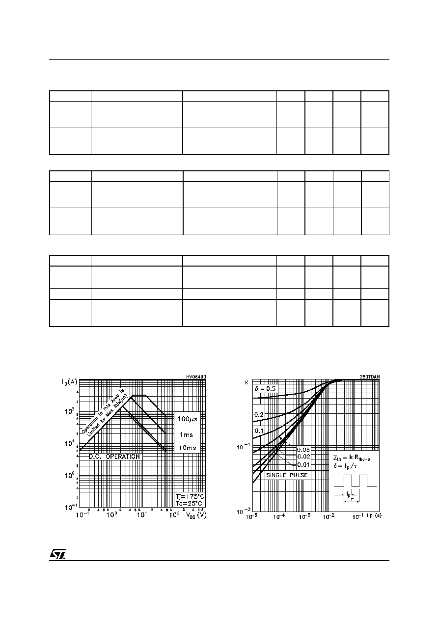
Thermal Impedance
Safe Operating Area
STW80NF55-08
4/8
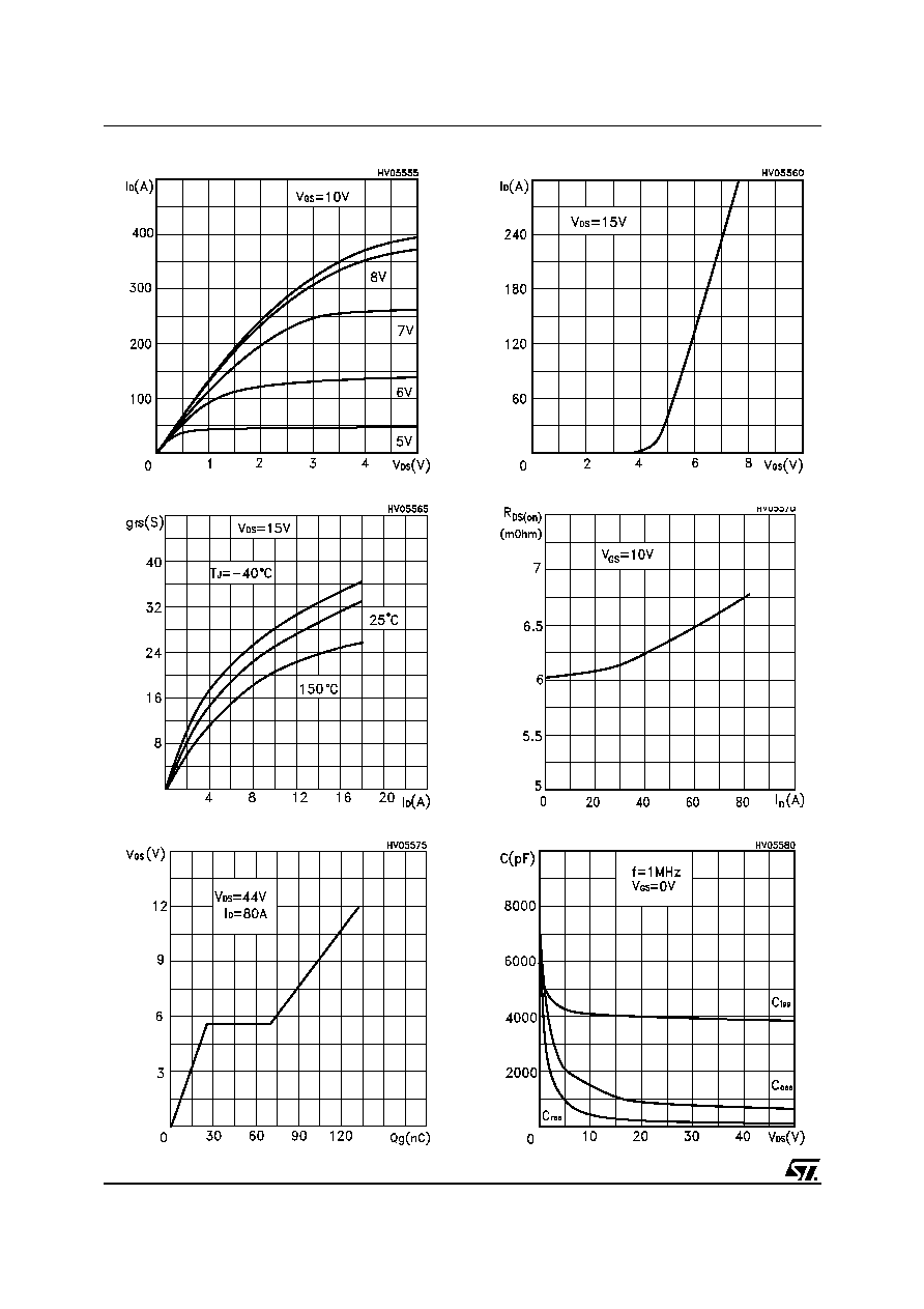
Gate Charge vs Gate-source Voltage
Tranconductance
Output Characteristics
Capacitance Variations
Tranfer Characteristics
Static Drain-Source On Resistance
5/8
STW80NF55-08
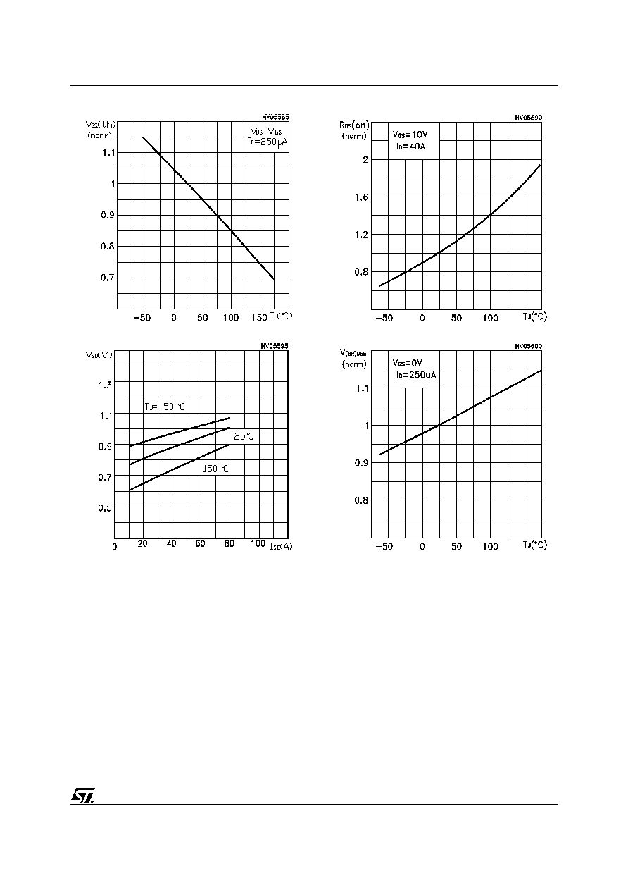
Normalized Breakdown Voltage vs Temperature
Normalized On Resistance vs Temperature
Normalized Gate Thereshold Voltage vs Temp.
Source-drain Diode Forward Characteristics
STW80NF55-08
6/8
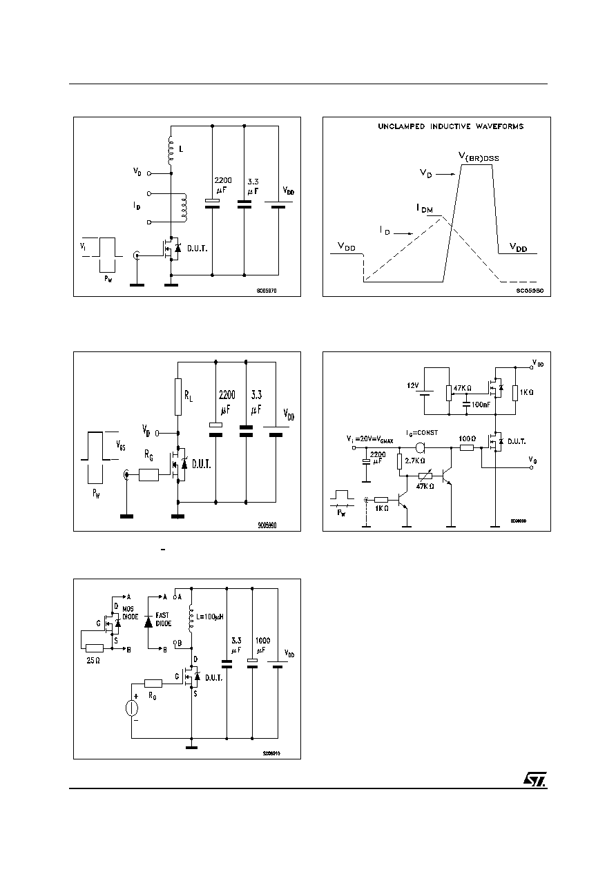
Fig. 5: Test Circuit For Inductive Load Switching
And Diode Recovery Times
Fig. 4: Gate Charge test Circuit
Fig. 2: Unclamped Inductive Waveform
Fig. 1: Unclamped Inductive Load Test Circuit
Fig. 3: Switching Times Test Circuit For
Resistive Load
7/8
STW80NF55-08
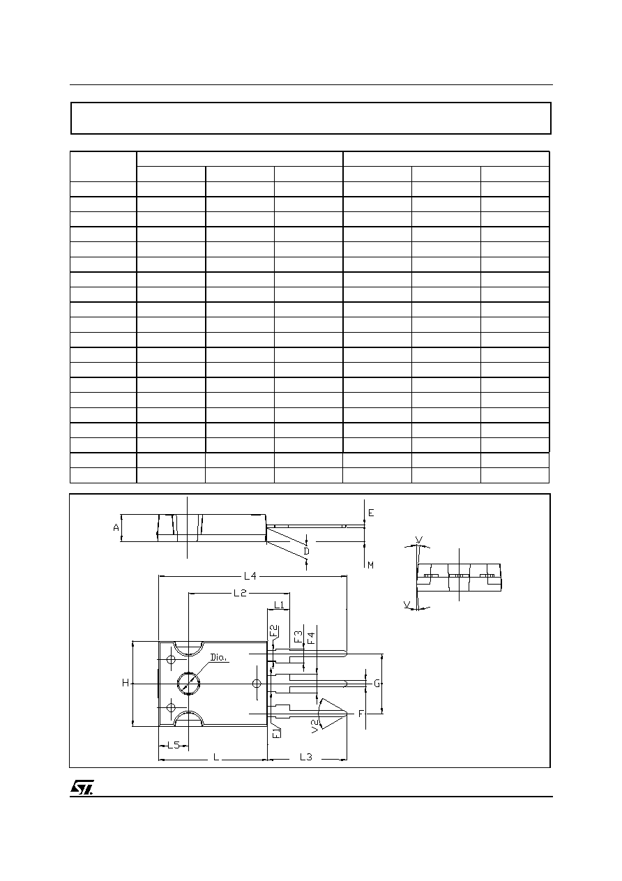
DIM.
mm.
inch
MIN.
TYP
MAX.
MIN.
TYP.
MAX.
A
4.85
5.15
0.19
0.20
D
2.20
2.60
0.08
0.10
E
0.40
0.80
0.015
0.03
F
1
1.40
0.04
0.05
F1
3
0.11
F2
2
0.07
F3
2
2.40
0.07
0.09
F4
3
3.40
0.11
0.13
G
10.90
0.43
H
15.45
15.75
0.60
0.62
L
19.85
20.15
0.78
0.79
L1
3.70
4.30
0.14
0.17
L2
18.50
0.72
L3
14.20
14.80
0.56
0.58
L4
34.60
1.36
L5
5.50
0.21
M
2
3
0.07
0.11
V
5∫
5∫
V2
60∫
60∫
Dia
3.55
3.65
0.14
0.143
TO-247 MECHANICAL DATA

STW80NF55-08
8/8
Information furnished is believed to be accurate and reliable. However, STMicroelectronics assumes no responsibility for the
consequences of use of such information nor for any infringement of patents or other rights of third parties which may result from
its use. No license is granted by implication or otherwise under any patent or patent rights of STMicroelectronics. Specifications
mentioned in this publication are subject to change without notice. This publication supersedes and replaces all information
previously supplied. STMicroelectronics products are not authorized for use as critical components in life support devices or
systems without express written approval of STMicroelectronics.
© The ST logo is a registered trademark of STMicroelectronics
© 2002 STMicroelectronics - Printed in Italy - All Rights Reserved
STMicroelectronics GROUP OF COMPANIES
Australia - Brazil - Canada - China - Finland - France - Germany - Hong Kong - India - Israel - Italy - Japan - Malaysia - Malta - Morocco
Singapore - Spain - Sweden - Switzerland - United Kingdom - United States.
© http://www.st.com