STZT2222
STZT2222A
MEDIUM POWER AMPLIFIER
ADVANCE DATA
s
SILICON EPITAXIAL PLANAR NPN
TRANSISTORS
s
MINIATURE PLASTIC PACKAGE FOR
APPLICATION IN SURFACE MOUNTING
CIRCUITS
s
GENERAL PURPOSE MAINLY INTENDED
FOR USE IN MEDIUM POWER INDUSTRIAL
APPLICATION AND FOR AUDIO AMPLIFIER
OUTPUT STAGE
s
PNP COMPLEMENTS ARE STZT2907 AND
STZT2907A RESPECTIVELY
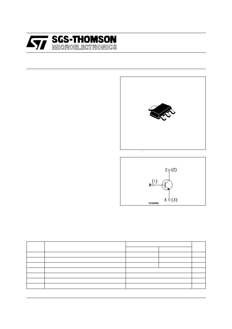
INTERNAL SCHEMATIC DIAGRAM
October 1995
ABSOLUTE MAXIMUM RATINGS
Symbol
Parameter
Value
Unit
STZT2222
STZT2222A
V
CBO
Collector-Base Voltage (I
E
= 0)
60
75
V
V
CEO
Collector-Emitter Voltage (I
B
= 0)
30
40
V
V
EBO
Emitter-Base Voltage (I
C
= 0)
5
6
V
I
C
Collector Current
0.8
A
P
tot
Total Dissipation at T
c
= 25
o
C
1.5
W
T
stg
Storage Temperature
-65 to 150
o
C
T
j
Max. Operating Junction Temperature
150
o
C
1
2
2
3
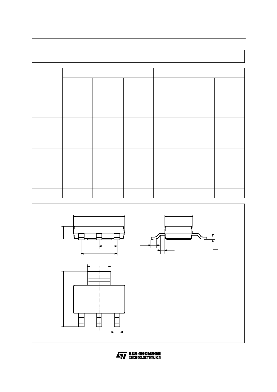
SOT-223
1/5
THERMAL DATA
R
th j-a mb
∑
R
thj-tab
∑
Thermal Resistance Junction-Ambient Max
Thermal Resistance Junction-Collecor Tab Max
83.3
10
o
C/W
o
C/W
∑
Mounted on a ceramic substrate area = 30 x 35 x 0.7 mm
ELECTRICAL CHARACTERISTICS (T
case
= 25
o
C unless otherwise specified)
Symbol
Parameter
Test Conditions
Min.
Typ.
Max.
Unit
I
CBO
Collector Cut-off
Current (I
E
= 0)
V
CB
= rated V
CBO
V
CB
= rated V
CBO
T
amb
= 125
o
C
10
10
nA
µ
A
I
CEX
Collector Cut-off
Current (V
BE
= -3V)
V
CE
= 60 V for STZT2222A
10
nA
I
BEX
Base Cut-off Current
(V
BE
= -3V)
V
CE
= 60 V for STZT2222A
20
nA
I
EBO
Emitter Cut-off Current
(I
E
= 0)
V
EB
= 3 V
for STZT2222
for STZT2222A
30
15
nA
nA
V
(BR)CBO
Collector-Base
Breakdown Voltage
(IE = 0)
I
C
= 10
µ
A
for STZT2222
for STZT2222A
60
75
V
V
V
(BR)CEO
Collector-Emitter
Breakdown Voltage
(I
B
= 0)
I
C
= 10 mA
for STZT2222
for STZT2222A
30
40
V
V
V
(BR)EBO
Emitter-Base
Breakdown Voltage
(I
C
= 0)
I
E
= 10
µ
A
for STZT2222
for STZT2222
5
6
V
V
V
CE(sat)
Collector-Emitter
Saturation Voltage
I
C
= 150 mA I
B
= 15 mA
for STZT2222
for STZT2222A
I
C
= 500 mA I
B
= 50 mA
for STZT2222
for STZT2222A
0.4
0.3
1.6
1
V
V
V
V
V
BE(sat)
Base-Emitter
Saturation Voltage
I
C
= 150 mA I
B
= 15 mA
for STZT2222
for STZT2222A
I
C
= 500 mA I
B
= 50 mA
for STZT2222
for STZT2222A
0.6
1.3
1.2
2.6
2
V
V
V
V
h
FE
DC Current Gain
I
C
= 0.1 mA V
CE
= 10 V
I
C
= 1 mA V
CE
= 10 V
I
C
= 10 mA V
CE
= 10 V
I
C
= 150 mA V
CE
= 10 V
I
C
= 150 mA V
CE
= 1 V
I
C
= 500 mA V
CE
= 10 V
for STZT2222
for STZT2222A
I
C
= 10 mA V
CE
= 10 V T
c
= -55
o
C
for STZT2222
35
50
75
100
50
30
40
35
300
STZT2222/STZT2222A
2/5
ELECTRICAL CHARACTERISTICS (T
case
= 25
o
C unless otherwise specified)
Symbol
Parameter
Test Conditions
Min.
Typ.
Max.
Unit
h
fe
Small Signal Current
Gain
I
C
= 1 mA V
CE
= 10 V f = 1 KHz
I
C
= 10 mA V
CE
= 10 V f = 1 KHz
50
75
300
375
K
h
ie
Input Impedance
I
C
= 1 mA V
CE
= 10 V f = 1 KHz
I
C
= 10 mA V
CE
= 10 V f = 1 KHz
2
0.25
8
1.25
h
re
Reverse Voltage Ratio
I
C
= 1 mA V
CE
= 10 V f = 1 KHz
I
C
= 10 mA V
CE
= 10 V f = 1 KHz
8
4
10
-4
h
oe
Output Impedance
I
C
= 1 mA V
CE
= 10 V f = 1 KHz
I
C
= 10 mA V
CE
= 10 V f = 1 KHz
5
25
35
375
S
f
T
Transition Frequency
I
C
= 10 mA V
CE
= 10 V f = 100 MHz
for STZT2222
for STZT2222A
250
300
MHz
MHz
C
CBO
Collector-Base
Capacitance
I
E
= 0 V
CB
= 10 V f = 1 MHz
8
pF
C
EBO
Emitter-Base
Capacitance
I
C
= 0 V
EB
= 0.5 V f = 1 MHz
for STZT2222
for STZT2222A
30
25
pF
pF
NF
Noise Figure
f = 1 KHz
F = 200 Hz R
G
= 1K
I
C
= 0.1 mA V
CE
= 10 V
4
dB
t
d
Delay Time
I
C
= 150 mA I
C1
= 15 mA
V
BE
= -0.5 V
10
ns
t
r
Rise Time
25
ns
t
s
Storage Time
I
C
= 150 mA I
C1
= 15 mA
I
B2
= 15 mA
225
ns
t
f
Fall Time
60
ns
Pulsed: Pulse duration = 300
µ
s, duty cycle
1.5 %
Only for STZT2222A
STZT2222/STZT2222A
3/5

Information furnished is believed to be accurate and reliable. However, SGS-THOMSON Microelectronics assumes no responsability for the
consequences of use of such information nor for any infringement of patents or other rights of third parties which may results from its use. No
license is granted by implication or otherwise under any patent or patent rights of SGS-THOMSON Microelectronics. Specifications mentioned
in this publication are subject to change without notice. This publication supersedes and replaces all information previously supplied.
SGS-THOMSON Microelectronics products are not authorized for use as critical components in life support devices or systems without express
written approval of SGS-THOMSON Microelectonics.
© 1995 SGS-THOMSON Microelectronics - All Rights Reserved
SGS-THOMSON Microelectronics GROUP OF COMPANIES
Australia - Brazil - France - Germany - Hong Kong - Italy - Japan - Korea - Malaysia - Malta - Morocco - The Netherlands -
Singapore - Spain - Sweden - Switzerland - Taiwan - Thailand - United Kingdom - U.S.A
.
STZT2222/STZT2222A
5/5