 | –≠–ª–µ–∫—Ç—Ä–æ–Ω–Ω—ã–π –∫–æ–º–ø–æ–Ω–µ–Ω—Ç: T0609MH | –°–∫–∞—á–∞—Ç—å:  PDF PDF  ZIP ZIP |
T0605xH
T0609xH
Æ
January 1995
SENSITIVE GATE TRIACS
Symbol
Parameter
Value
Unit
I
T(RMS)
RMS on-state current
(360
∞
conduction angle)
Tc= 100
∞
C
6
A
I
TSM
Non repetitive surge peak on-state current
(T
j
initial = 25
∞
C )
tp = 8.3 ms
63
A
tp = 10 ms
60
I
2
t
I
2
t Value for fusing
tp = 10 ms
18
A
2
s
dI/dt
Critical rate of rise of on-state current
I
G
= 50 mA
di
G
/dt = 0.1 A/
µ
s.
Repetitive
F = 50 Hz
10
A/
µ
s
Non
Repetitive
50
T
stg
T
j
Storage and operating junction temperature range
- 40, + 150
- 40, + 125
∞
C
Tl
Maximum lead temperature for soldering during 10s at
4.5mm from case
260
∞
C
ABSOLUTE RATINGS (limiting values)
I
T(RMS)
= 6A
V
DRM
= 400V to 800V
I
GT
5mA to
10mA
FEATURES
Symbol
Parameter
Voltage
Unit
D
M
S
N
V
DRM
V
RRM
Repetitive peak off-state voltage
T
j
= 125
∞
C
400
600
700
800
V
The T06xxxH series of triacs uses a high
performance MESA GLASS technology. These
parts
are
intended
for
general
purpose
applications where
gate
high
sensitivity is
required.
DESCRIPTION
A1
G
A2
TO220
non-insulated
(Plastic)
1/5

P
G (AV)
= 1 W P
GM
= 10 W (tp = 20
µ
s)
I
GM
= 4 A (tp = 20
µ
s)
GATE CHARACTERISTICS (maximum values)
Symbol
Parameter
Value
Unit
Rth(j-a)
Junction to ambient
60
∞
C/W
Rth(j-c)
Junction to case for D.C
4
∞
C/W
Rth(j-c)
Junction to case for A.C 360
∞
conduction angle (F=50Hz)
3
∞
C/W
THERMAL RESISTANCES
Symbol
Test Conditions
Quadrant
Sensitivity
Unit
05
09
I
GT
V
D
=12V (DC) R
L
=33
Tj= 25
∞
C
I-II-III-IV
MAX
5
10
mA
V
GT
V
D
=12V (DC) R
L
=33
Tj= 25
∞
C
I-II-III-IV
MAX
1.5
V
V
GD
V
D
=V
DRM
R
L
=3.3k
Tj= 125
∞
C
I-II-III-IV
MIN
0.2
V
tgt
V
D
=V
DRM
I
G
= 40mA
I
T
= 8.5A
dI
G
/dt = 0.5A/
µ
s
Tj= 25
∞
C
I-II-III-IV
TYP
2
µ
s
I
H
*
I
T
= 50mA Gate open
Tj= 25
∞
C
MAX
5
10
mA
I
L
I
G
= 1.2 I
GT
Tj= 25
∞
C
I-III-IV
TYP
5
10
mA
II
TYP
10
20
V
TM
*
I
TM
= 8.5A tp= 380
µ
s
Tj= 25
∞
C
MAX
1.65
V
I
DRM
I
RRM
V
D
= V
DRM
V
R
= V
RRM
Tj= 25
∞
C
MAX
5
µ
A
Tj= 110
∞
C
MAX
2
mA
dV/dt *
VD=67%V
DRM
Gate open
Tj= 110
∞
C
MIN
20
V/
µ
s
TYP
10
(dV/dt)c *
(dI/dt)c = 2.7 A/ms
Tj= 110
∞
C
TYP
1
2
V/
µ
s
* For either polarity of electrode A
2
voltage with reference to electrode A
1
ELECTRICAL CHARACTERISTICS
ORDERING INFORMATION
T
06
09
M
H
TRIAC MESA GLASS
CURRENT
PACKAGE :
H = TO220 Non-insulated
VOLTAGE
SENSITIVITY
Æ
T0605xH / T0609xH
2/5
0
1
2
3
4
5
6
0
2
4
6
8
10
180
O
= 180
o
= 120
o
= 90
o
= 60
o
= 30
o
T(RMS)
I
(A)
P(W)
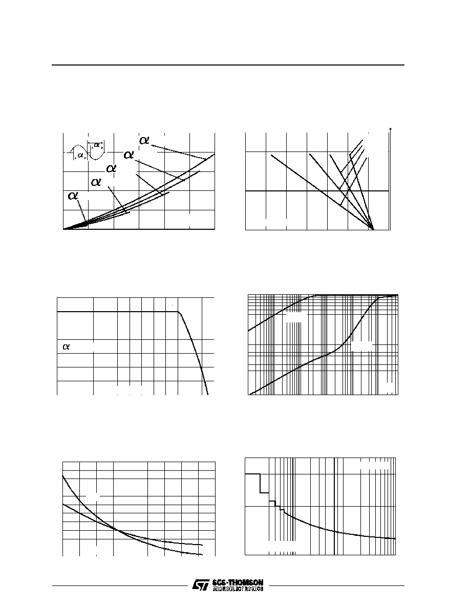
Fig.1 : Maximum RMS power dissipation versus
RMS on-state current.
0
10 20 30 40 50 60 70 80 90 100 110 120 130
0
1
2
3
4
5
6
7
= 180
o
Tcase( C)
o
I
(A)
T(RMS)
Fig.3 : RMS on-state current versus case tempera-
ture.
2.6
2.4
2.2
2.0
1.8
1.6
1.4
1.2
1.0
0.8
0.6
0.4
Igt
Tj( C)
o
Ih
-40
-20
0
20
40
60
80
100
120 140
Igt[Tj]
Igt[Tj=25 C]
o
Ih[Tj]
Ih[Tj=25 C]
o
Fig.5 : Relative variation of gate trigger current and
holding current versus junction temperature.
0
20
40
60
80
100
120
140
0
2
4
6
8
10
-95
-100
-105
-110
-115
-120
-125
P (W)
Rth = 0 C/W
2.5 C/W
5 C/W
10 C/W
o
o
o
o
Tamb ( C)
o
Tcase ( C)
o
Fig.2 : Correlation between maximum RMS power
dissipation and maximum allowable temperature
(Tamb and Tcase) for different thermal resistances
heatsink + contact.
1E-3
1E-2
1E-1
1E +0
1 E +1
1E +2 5 E+2
0.01
0.1
1
Zth/Rth
Zt h( j-c )
Zt h( j-a )
tp (s )
Fig.4 : Relative variation of thermal impedance
versus pulse duration.
1
10
100
100 0
0
10
20
30
40
50
60
Tj initial = 25 C
o
Number of cycles
I
(A)
TSM
Fig.6 : Non repetitive surge peak on-state current
versus number of cycles.
Æ
T0605xH / T0609xH
3/5
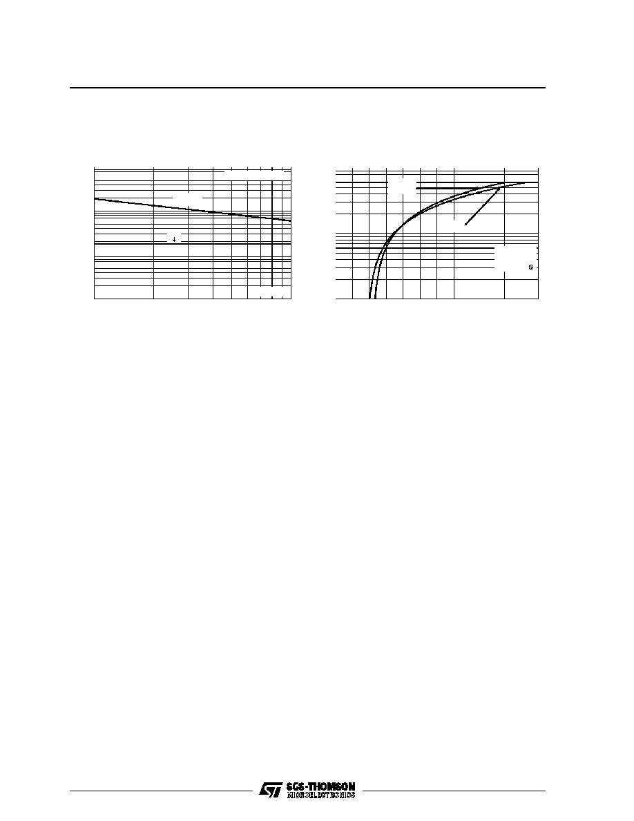
1
10
1
10
100
1000
I
(A). I
2
t (A
2
s)
TSM
Tj initial = 25 C
o
ITSM
t (ms)
I
2
t
Fig.7 : Non repetitive surge peak on-state current
for a sinusoidal pulse with width : t
10ms, and cor-
responding value of I
2
t.
0
0.5
1
1.5
2
2.5
3
3.5
4
4.5
5
5.5
6
1
10
100
I
(A)
TM
Tj in itial
25 C
o
Tj max
V
(V)
TM
Tj max
Vto =0. 93V
Rt =0.0 78
Fig.8 : On-state characteristics (maximum values).
Æ
T0605xH / T0609xH
4/5
Information furnished is believed to be accurate and reliable. However, SGS-THOMSON Microelectronics assumes no responsability for the
consequences of use of such information nor for any infringement of patents or other rights of third parties which may result from its use. No
license is granted by implication or otherwise under any patent or patent rights of SGS-THOMSON Microelectronics. Specifications mentioned
in this publication are subject to change without notice. This publication supersedes and replaces all information previously supplied.
SGS-THO MSON Microelectronics products are not authorized for use as critical components in life support devices or systems without express
written approval of SGS-THOMSON Microelectronics.
©
1995 SGS-THOMSON Microelectronics - All rights reserved.
SGS-THOMSON Microelectronics GROUP OF COMPANIES
Australia - Brazil - France - Germany - Hong Kong - Italy - Japan - Korea - Malaysia - Malta - Morocco - The Netherlands
Singapore - Spain - Sweden - Switzerland - Taiwan - Thailand - United Kingdom - U.S.A.
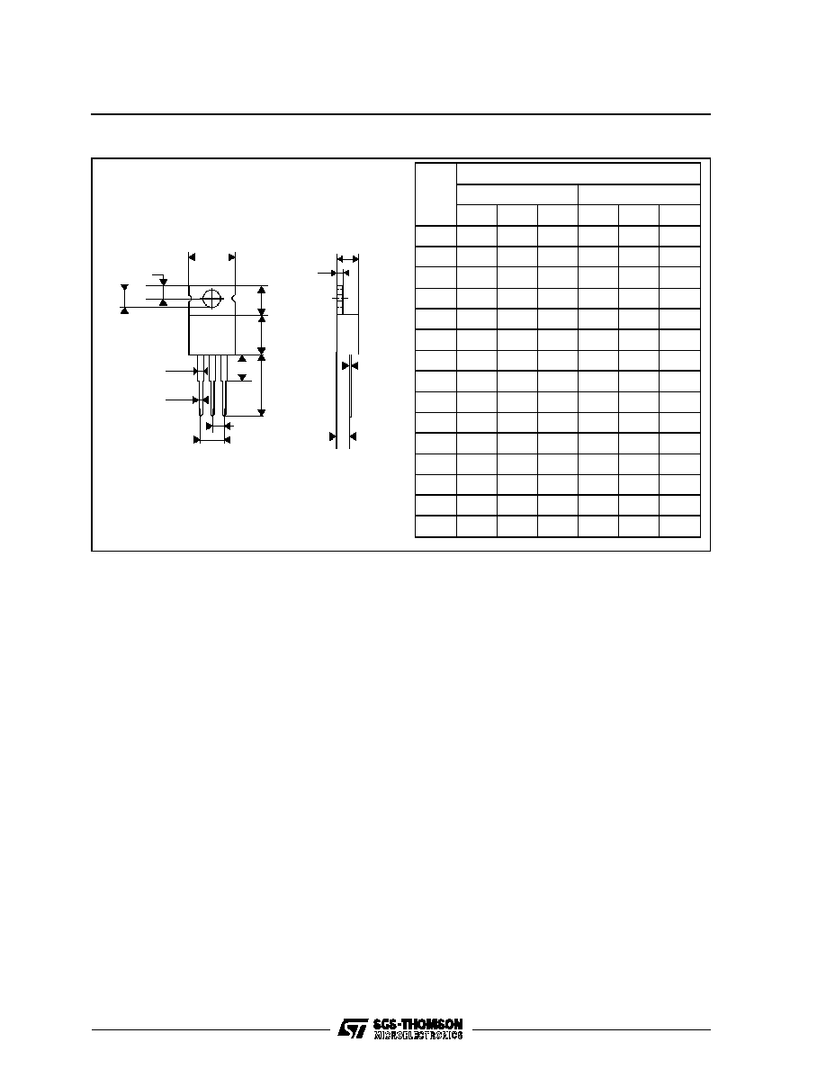
PACKAGE MECHANICAL DATA
TO220 Non-insulated (Plastic)
D
G
I
H
J
B
A
L
N1
M
N
O
P
C
F
REF.
DIMENSIONS
Millimeters
Inches
Typ.
Min. Max. Typ.
Min. Max.
A
10.3
0.406
B
6.3
6.5
0.248 0.256
C
9.1
0.358
D
12.7
0.500
F
4.2
0.165
G
3.0
0.118
H
4.5
4.7
0.177 0.185
I
3.53
3.66
0.139 0.144
J
1.2
1.3
0.047 0.051
L
0.9
0.035
M
2.7
0.106
N
5.3
0.209
N1
2.54
0.100
O
1.2
1.4
0.047 0.055
P
1.15
0.045
Marking : type number
Weight : 1.8 g
Æ
T0605xH / T0609xH
5/5