1/5
T1020-600W
T1030-600W
Æ
September 2001 - Ed: 1A
SNUBBERLESS TRIAC
Symbol
Parameter
Value
Unit
I
T(RMS)
RMS on-state current
(360∞ conduction angle)
Tc= 90∞C
10
A
I
TSM
Non repetitive surge peak on-state current
(T
j
initial = 25∞C )
tp = 16.7 ms
(1 cycle, 60 Hz)
110
A
tp = 10 ms
(1/2 cycle, 50 Hz)
125
I
2
t
I
2
t Value (half-cycle, 50 Hz)
tp = 10 ms
78
A
2
s
dI/dt
Critical rate of rise of on-state current
Gate supply : I
G
= 500 mA
dI
G
/dt = 1 A/
µ
s.
Repetitive
F = 50 Hz
20
A/
µ
s
Non Repetitive
100
T
stg
T
j
Storage temperature range
Operating junction temperature range
- 40 to + 150
- 40 to + 125
∞C
ABSOLUTE RATINGS (limiting values)
s
I
TRMS
= 10 A
s
V
DRM
= V
RRM
= 600V
s
EXCELLENT SWITCHING PERFORMANCES
s
INSULATING VOLTAGE = 1500V
(RMS)
s
U.L. RECOGNIZED : E81734
FEATURES
Symbol
Parameter
Value
Unit
V
DRM
V
RRM
Repetitive peak off-state voltage
T
j
= 125∞C
600
V
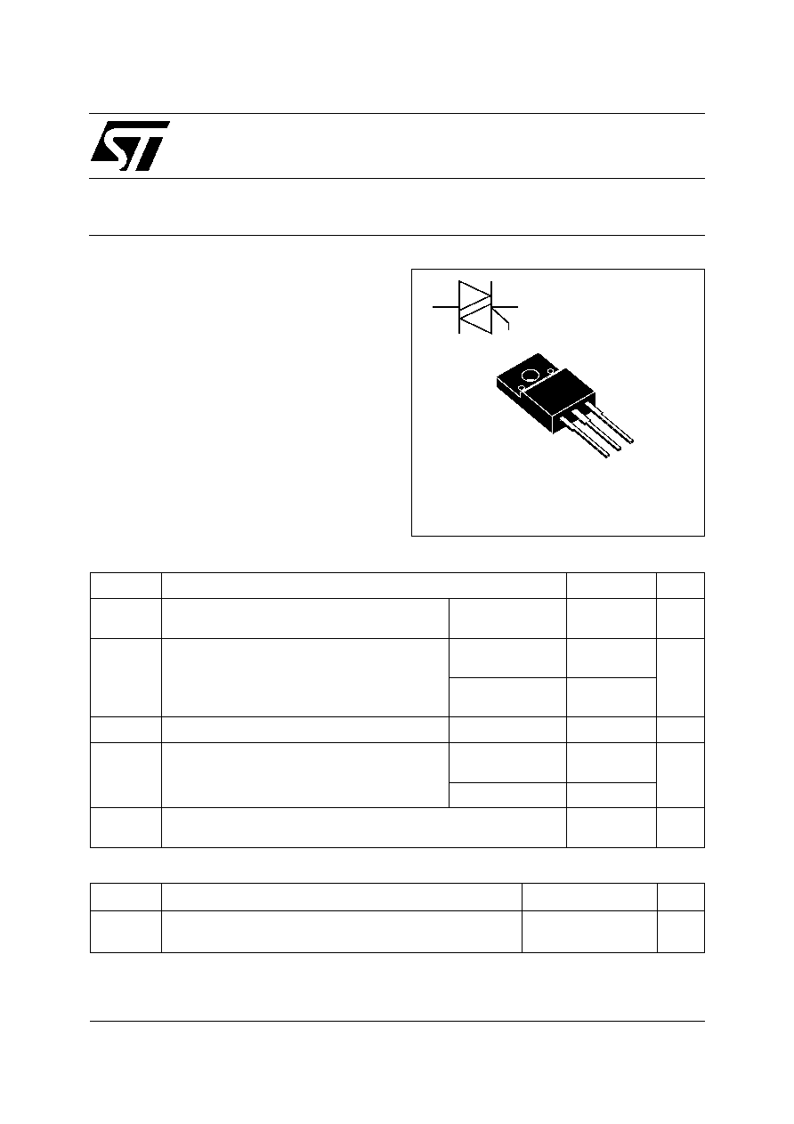
The T1020-600W and 1030-600W triacs use high
performance glass passivated chip technology,
housed in a fully molded plastic ISOWATT220AB
package.
The SNUBBERLESS
TM
concept offers suppres-
sion of R-C network, and is suitable for applica-
tions such as phase control and static switch on
inductive and resistive loads.
DESCRIPTION
ISOWATT220AB
(Plastic)
A1
A2
G
A
1
A
2
G
T1020-600W / 1030-600W
2/5
P
G (AV)
= 100 mW P
GM
= 2 W (tp = 20
µ
s)
I
GM
= 1 A (tp = 20
µ
s)
GATE CHARACTERISTICS (maximum values)
Symbol
Parameter
Value
Unit
Rth(j-a)
Junction to ambient
50
∞
C/W
Rth(j-c)
Junction to case for A.C (360∞ conduction angle)
3.0
∞
C/W
THERMAL RESISTANCES
Symbol
Test Conditions
Quadrant
T1020
T1030
Unit
I
GT
V
D
=12V (DC) R
L
=33
Tj= 25∞C
I-II-III
MAX
20
30
mA
V
GT
V
D
=12V (DC) R
L
=33
Tj= 25
∞
C
I-II-III
MAX
1.5
V
V
GD
V
D
=V
DRM
R
L
=3.3k
Tj= 125∞C
I-II-III
MIN
0.2
V
tgt
V
D
=V
DRM
I
G
=500mA
dl
G
/dt= 3A
µ
s
Tj= 25∞C
I-II-III
TYP
2
µ
s
I
H
*
I
T
= 100mA
Gate open
Tj= 25
∞
C
MAX
35
50
V
TM
*
I
TM
= 14A tp= 380
µ
s
Tj= 25
∞
C
MAX
1.5
V
I
DRM
I
RRM
V
DRM
rated
V
RRM
rated
Tj= 25∞C
MAX
10
µ
A
Tj= 125∞C
MAX
2
mA
dV/dt *
Linear slope up to
V
D
=67%V
DRM
Gate open
Tj= 125
∞
C
MIN
200
300
V/
µ
s
(dV/dt)c *
(dI/dt)c = 5.3 A/ms (see note)
Tj= 125
∞
C
MIN
10
20
V/
µ
s
* For either polarity of electrode A2 voltage with reference to electrode A1.
Note : In usual applications where (dI/dt)c is below 5.3 A/ms, the (dV/dt)c is always lower than 10V/
µ
s, and, therefore, it is unnecessary to use
a snuber R-C network accross T1020W / T1030W triacs.
ELECTRICAL CHARACTERISTICS
T1020-600W / 1030-600W
3/5
0
1
2
3
4
5
6
7
8
9
10
0
2
4
6
8
10
12
14
180
O
= 180
o
= 120
o
= 90
o
= 60
o
= 30
o
T(RMS)
I
(A)
P(W)
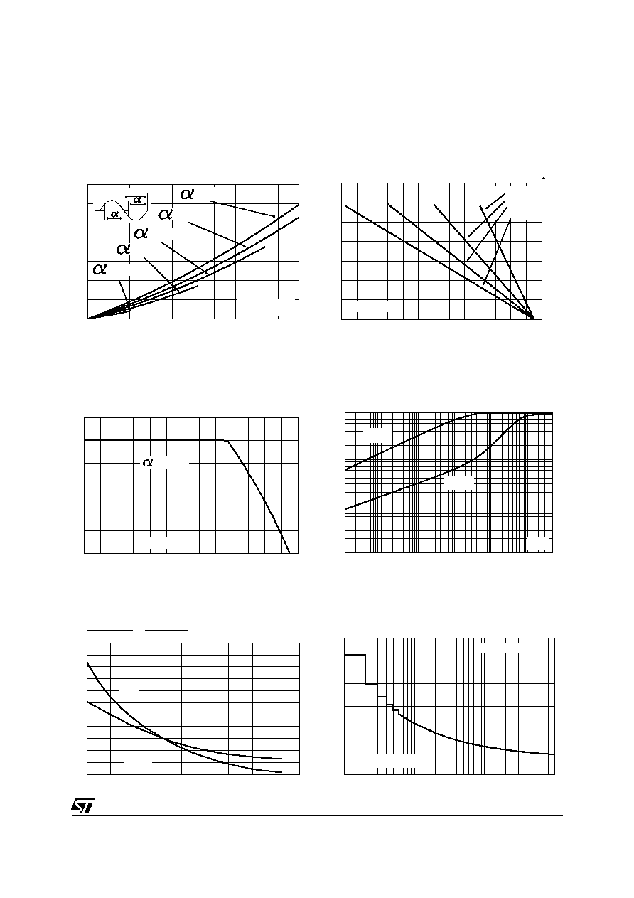
Fig.1 : Maximum power dissipation versus RMS
on-state current.
0
10
20
30
40
50
60
70
80
90 100 110 120 130
0
2
4
6
8
10
12
= 180
o
Tcase( C)
o
I
(A)
T(RMS)
Fig.3 : RMS on-state current versus case temper-
ature.
2.6
2.4
2.2
2.0
1.8
1.6
1.4
1.2
1.0
0.8
0.6
0.4
Igt
Tj( C)
o
Ih
-40
-20
0
20
40
60
80
100
120
140
Igt[Tj]
Igt[Tj=25 C]
o
Ih[Tj]
Ih[Tj=25 C]
o
Fig.5 : Relative variation of gate trigger current
and holding current versus junction temperature.
P (W)
0
10 20 30 40 50 60 70 80 90 100 110 120 130
0
2
4
6
8
10
12
14
-85
-95
-105
-115
-125
Rth = 0 C/W
2.5 C/W
5 C/W
7 C/W
o
o
o
o
Tamb ( C)
o
Tcase ( C)
o
Fig.2 : Correlation between maximum power dissi-
pation and maximum allowable temperature
(Tamb and Tcase) for different thermal resistances
heatsink + contact.
1E-3
1E-2
1E-1
1E +0
1E +1
1E+2 5E+2
0.01
0.1
1
Zth/Rth
Zth(j-c)
Zth(j-a)
tp(s)
Fig.4 : Thermal transient impedance junction to
case and junction to ambient versus pulse dura-
tion.
1
10
100
1000
0
20
40
60
80
100
120
Tj initial = 25 C
o
Number of cycles
I
(A)
TSM
Fig.6 : Non repetitive surge peak on-state current
versus number of cycles.
T1020-600W / 1030-600W
4/5
I
(A). I
2
t (A
2
s)
TSM
1
10
1
10
100
1000
Tj initial = 25 C
o
I
TSM
tp(ms)
I
2
t
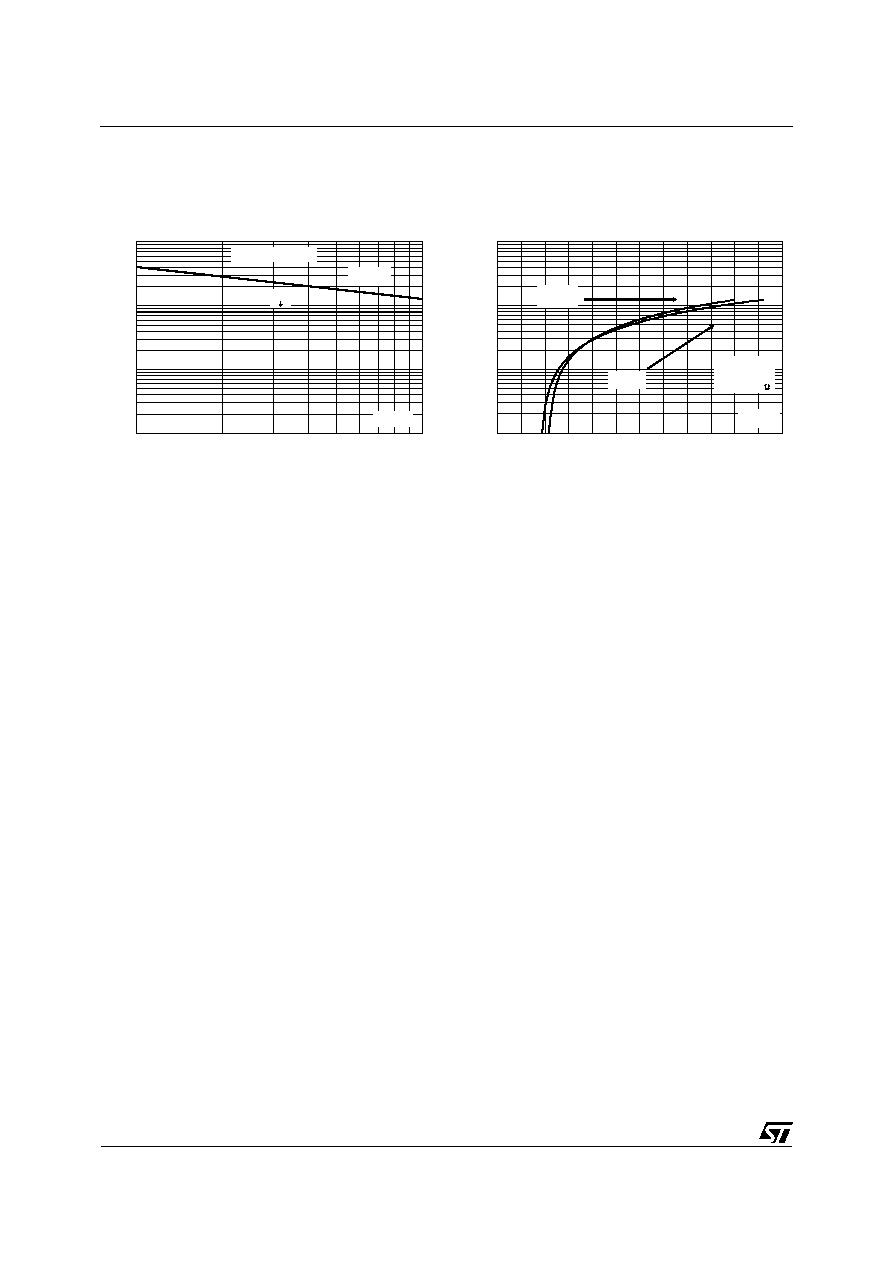
Fig.7 : Non repetitive surge peak on-state current
for a sinusoidal pulse with width : tp
Æ
10ms, and
corresponding value of I
2
t.
0
0.5
1
1.5
2
2.5
3
3.5
4
4.5
5
5.5
6
1
10
100
1000
I
(A)
TM
Tj initial
25 C
o
Tj max
Tj max
Vto =0.9V
Rt =0.038
V
(V)
TM
Fig.8 : On-state characteristics (maximum val-
ues).
T1020-600W / 1030-600W
5/5
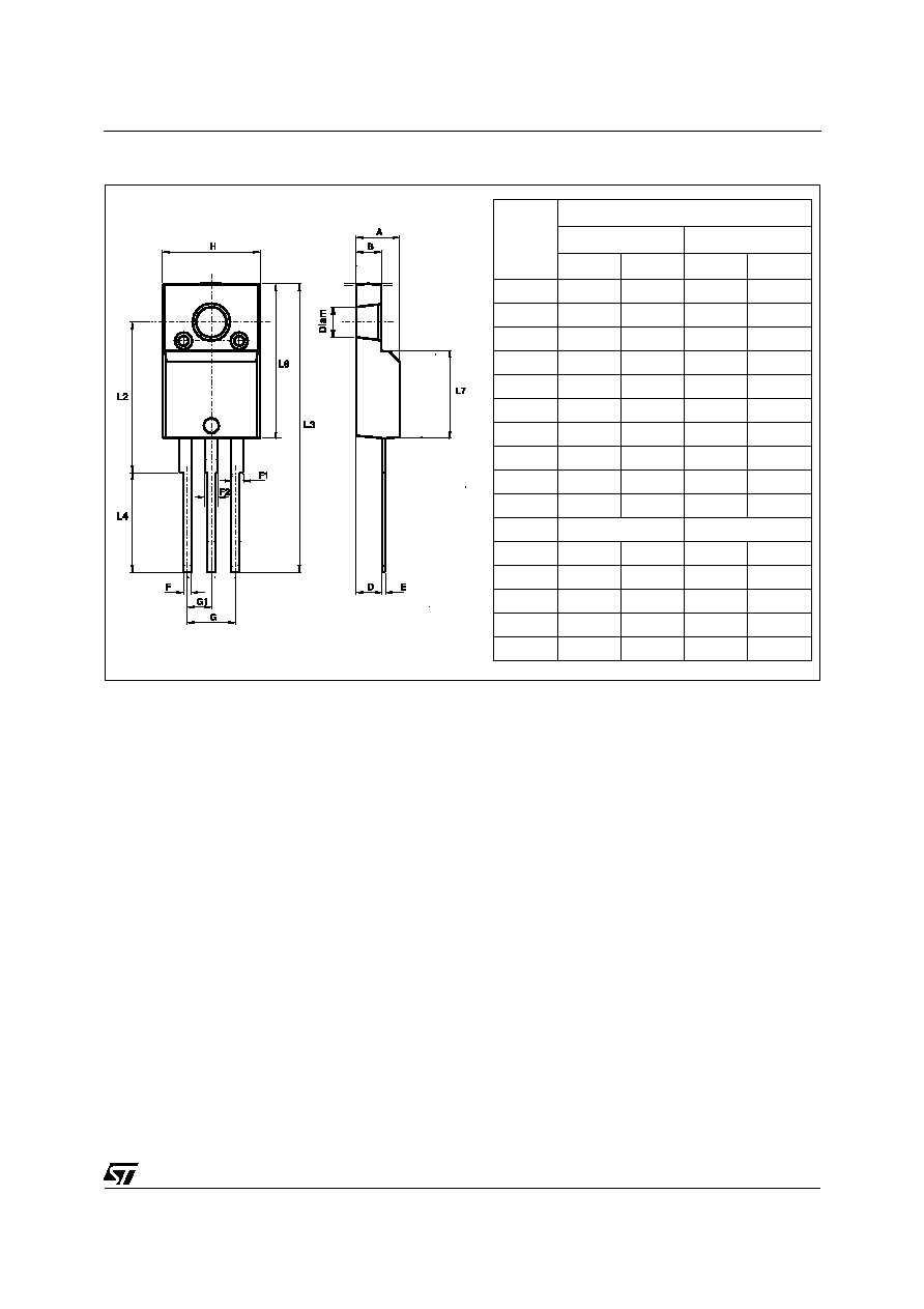
PACKAGE MECHANICAL DATA
ISOWATT220AB
s
Cooling method: C
s
Marking: Type number
s
Weight: 2.1 g
s
Recommended torque value: 0.55 m.N.
s
Maximum torque value: 0.70 m.N.
Information furnished is believed to be accurate and reliable. However, STMicroelectronics assumes no responsibility for the consequences of
use of such information nor for any infringement of patents or other rights of third parties which may result from its use. No license is granted by
implication or otherwise under any patent or patent rights of STMicroelectronics. Specifications mentioned in this publication are subject to
change without notice. This publication supersedes and replaces all information previously supplied.
STMicroelectronics products are not authorized for use as critical components in life support devices or systems without express written ap-
proval of STMicroelectronics.
The ST logo is a registered trademark of STMicroelectronics
© 2001 STMicroelectronics - Printed in Italy - All rights reserved.
STMicroelectronics GROUP OF COMPANIES
Australia - Brazil - China - Finland - France - Germany - Hong Kong - India - Italy - Japan - Malaysia
Malta - Morocco - Singapore - Spain - Sweden - Switzerland - United Kingdom - U.S.A.
http://www.st.com
REF.
DIMENSIONS
Millimeters
Inches
Min.
Max.
Min.
Max.
A
4.40
4.60
0.173
0.181
B
2.50
2.70
0.098
0.106
D
2.50
2.75
0.098
0.108
E
0.40
0.70
0.016
0.028
F
0.75
1.00
0.030
0.039
F1
1.15
1.70
0.045
0.067
F2
1.15
1.70
0.045
0.067
G
4.95
5.20
0.195
0.205
G1
2.40
2.70
0.094
0.106
H
10.00
10.40
0.394
0.409
L2
16.00 typ.
0.630 typ.
L3
28.60
30.60
1.125
1.205
L4
9.80
10.60
0.386
0.417
L6
15.90
16.40
0.626
0.646
L7
9.00
9.30
0.354
0.366
Diam
3.00
3.20
0.118
0.126