T1635-600G
T1650-600G
ģ
May 1998 - Ed: 2A
HIGH PERFORMANCE TRIAC
Symbol
Parameter
Value
Unit
V
DRM
V
RRM
Repetitive peak off-state voltage
Tj = 125įC
600
V
I
T(RMS)
RMS on-state current
(360
į
conduction angle)
Tc= 105įC
16
A
I
TSM
Non repetitive surge peak on-state current
(Tj initial = 25įC)
tp = 8.3ms
170
A
tp = 10 ms
160
I
2
t
I
2
t Value for fusing
tp = 10 ms
128
A
2
s
dI/dt
Critical rate of rise of on-state current
I
G
= 500 mA dI
G
/dt = 1 A/
Ķ
s.
Repetitive
F = 50 Hz
20
A/
Ķ
s
Non Repetitive
100
T
stg
T
j
Storage temperature range
Operating junction temperature range
- 40, + 150
- 40, + 125
į
C
T
Maximum temperature for soldering during 10s
260
į
C
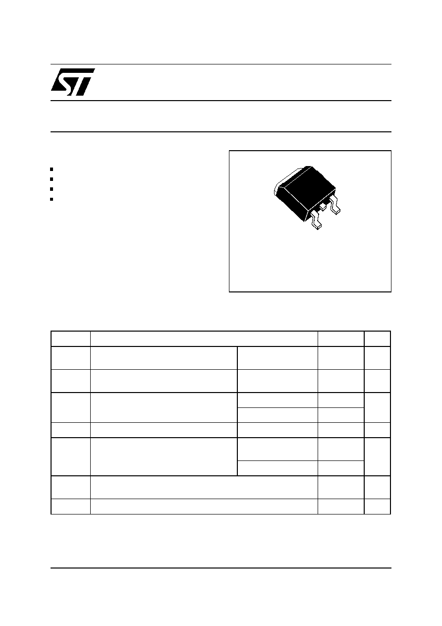
ABSOLUTE RATINGS (limiting values)
D
2
PAK
HIGH COMMUTATION PERFORMANCES
SNUBBERLESS
TM
TECHNOLOGY
HIGH NOISE IMMUNITY (dV/dt)
HIGH I
TSM
FEATURES
The T1635-600G and T1650-600G triacs are
using high performance SNUBBERLESS
technology.
They are intended for AC control applications
using surface mount technology.
These devices are perfectly suited where high
commutation and surge performances are
required.
DESCRIPTION
A1
A2
G
A2
1/5
P
G (AV)
= 1 W P
GM
= 10 W (tp = 20
Ķ
s) I
GM
= 4 A (tp = 20
Ķ
s)
GATE CHARACTERISTICS (maximum values)
Symbol
Parameter
Value
Unit
Rth(j-a)
Junction to ambient (S=1cm
2
)
45
įC/W
Rth(j-c)
Junction to case for DC
1.6
į
C/W
Rth(j-c)
Junction to case for AC 360į conduction angle (F=50Hz)
1.2
į
C/W
THERMAL RESISTANCES
Symbol
Test Conditions
Quadrant
T1635 T1650
Unit
I
GT
V
D
=12V (DC) R
L
=33
Tj= 25
į
C
I-II-III
MIN
2
mA
MAX
35
50
V
GT
V
D
=12V (DC) R
L
=33
Tj= 25
į
C
I-II-III
MAX
1.3
V
V
GD
V
D
=V
DRM
R
L
=3.3k
Tj= 125
į
C
I-II-III
MIN
0.2
V
I
H
*
I
T
= 100mA Gate open
Tj= 25
į
C
MAX
35
50
mA
I
L
I
G
= 1.2 I
GT
Tj = 25įC
I-III
MAX
50
60
mA
II
MAX
80
120
V
TM *
I
TM
= 22.5A tp= 380
Ķ
s
Tj= 25
į
C
MAX
1.5
V
I
DRM
VD = V
DRM
Tj= 25
į
C
MAX
5
Ķ
A
I
RRM
V
R
= V
RRM
Tj= 125įC
MAX
2
mA
dV/dt *
Linear slope up to V
D
=67%V
DRM
Gate open
Tj= 125
į
C
MIN
500
1000
V/
Ķ
s
(dI/dt)c *
Without snubber
Tj= 125
į
C
MIN
8.5
14
A/ms
* For either polarity of electrode A2 voltage with reference to electrode A1.
ELECTRICAL CHARACTERISTICS
ORDERING INFORMATION
T 16 35 - 600 G
TRIAC
CURRENT
PACKAGE :
G = D
2
PAK
VOLTAGE
SENSITIVITY
Add "-TR" suffix for Tape & Reel shipment
T1635-600G / T1650-600G
2/5
0
2
4
6
8
10
12
14
16
0
5
10
15
20
P(W)
=180į
=120į
=90į
=60į
=30į
I
(A)
T(RMS)
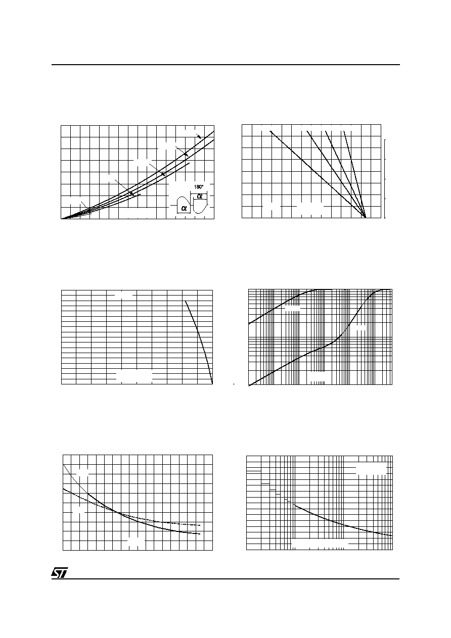
Fig 1: Maximum power dissipation versus RMS
on-state current.
0
25
50
75
100
125
0
2
4
6
8
10
12
14
16
18
I
(A)
T(RMS)
=180į
Tcase(įC)
Fig. 3: RMS on-state current versus case tem-
perature.
-40
-20
0
20
40
60
80
100
120
140
0.0
0.5
1.0
1.5
2.0
2.5
I ,I [Tj]/I ,I [Tj=25įC]
GT H
GT H
I
GT
I
H
Tj(įC)
Fig. 5: Relative variation of gate trigger current and
holding current versus junction temperature (typi-
cal values).
0
20
40
60
80
100
120
140
0
5
10
15
20
P(W)
Tcase (įC)
125
=180į
Rth=0įC/W
Rth=1įC/W
Rth=2įC/W
Rth=4įC/W
105
110
115
120
Tamb(įC)
Fig. 2: Correlation between maximum power dissi-
pation and maximum allowable temperatures
(T
amb
and T
case
) for different thermal resistances
heatsink+contact.
1E-3
1E-2
1E-1
1E+0
1E+1
1E+2 5E+2
0.01
0.10
1.00
K=[Zth/Rth]
Zth(j-c)
Zth(j-a)
tp(s)
Fig. 4: Relative variation of thermal impedance
versus pulse duration.
1
10
100
1000
0
20
40
60
80
100
120
140
160
I
(A)
TSM
Tj initial=25įC
F=50Hz
Number of cycles
Fig. 6: Non repetitive surge peak on-state current
versus number of cycles.
T1635-600G / T1650-600G
3/5
1
2
5
10
100
200
500
1000
I
(A),I≤t(A≤s)
TSM
Tj initial=25įC
I
TSM
I≤t
tp(ms)
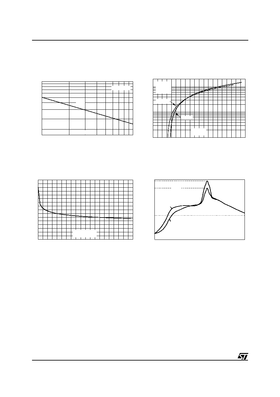
Fig. 7: Non repetitive surge peak on-state current
for a sinusoidal pulse with width tp<10ms, and cor-
responding value of I
2
t.
0
4
8
12
16
20
24
28
32
36
40
0
10
20
30
40
50
60
70
80
Rth(j-a) (įC/W)
S(Cu) (cm≤)
Fig. 9: Thermal resistance junction to ambient ver-
sus copper surface under tab (Epoxy printed circuit
board FR4, copper thickness: 35
Ķ
m).
0.0 0.5 1.0 1.5 2.0 2.5 3.0 3.5 4.0 4.5 5.0
1
10
100
200
I (A)
TM
Tj=25įC
Tj max.:
Vto=0.77V
Rt=30 m
Tj=Tj max.
V (V)
TM
Fig. 8: On-state characteristics (maximum values).
0
40
80
120
160
200
240
280
320 360
T (įC)
250
200
150
100
50
0
Epoxy FR4
board
Metal-backed
board
245įC
215įC
t (s)
Fig. 10: Typical reflow soldering heat profile, either
for mounting on FR4 or metal-backed boards.
T1635-600G / T1650-600G
4/5
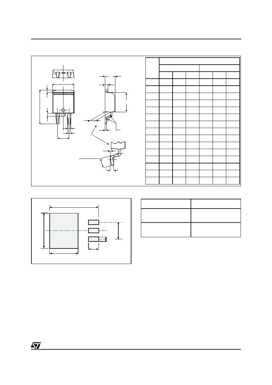
PACKAGE MECHANICAL DATA
D
2
PAK
A
C2
D
R
2.0 MIN.
FLAT ZONE
A2
V2
C
A1
G
L
L3
L2
B
B2
E
REF.
DIMENSIONS
Millimeters
Inches
Min. Typ. Max. Min. Typ. Max.
A
4.30
4.60 0.169
0.181
A1
2.49
2.69 0.098
0.106
A2
0.03
0.23 0.001
0.009
B
0.70
0.93 0.027
0.037
B2
1.25
1.40
0.048 0.055
C
0.45
0.60 0.017
0.024
C2
1.21
1.36 0.047
0.054
D
8.95
9.35 0.352
0.368
E
10.00
10.28 0.393
0.405
G
4.88
5.28 0.192
0.208
L
15.00
15.85 0.590
0.624
L2
1.27
1.40 0.050
0.055
L3
1.40
1.75 0.055
0.069
R
0.40
0.016
V2
0į
8į
0į
8į
Information furnished is believed to be accurate and reliable. However, STMicroelectronics assumes no responsibility for the consequences of
use of such information nor for any infringement of patents or other rights of third parties which may result from its use. No license is granted by
implication or otherwise under any patent or patent rights of STMicroelectronics. Specifications mentioned in this publication are subject to
change without notice. This publication supersedes and replaces all information previously supplied.
STMicroelectronics products are not authorized for use as critical components in life support devices or systems without express written ap-
proval of STMicroelectronics.
© 1998 STMicroelectronics - Printed in Italy - All rights reserved.
STMicroelectronics GROUP OF COMPANIES
Australia - Brazil - Canada - China - France - Germany - Italy - Japan - Korea - Malaysia - Malta - Mexico - Morocco - The
Netherlands - Singapore - Spain - Sweden - Switzerland - Taiwan - Thailand - United Kingdom - U.S.A.
FOOT PRINT DIMENSIONS (in millimeters)
TYPE
MARKING
T1635-600G
T1635
600G
T1650-600G
T1650
600G
MARKING
8.90
3.70
1.30
5.08
16.90
10.30
PACKING
Tube : 50 units
Tape and reel : 500 units
T1635-600G / T1650-600G
5/5