 | –≠–ª–µ–∫—Ç—Ä–æ–Ω–Ω—ã–π –∫–æ–º–ø–æ–Ω–µ–Ω—Ç: T410 | –°–∫–∞—á–∞—Ç—å:  PDF PDF  ZIP ZIP |
Rev. 1.6 - November 2002
1/84
PRELIMINARY DATASHEET
ST52T410/T420/E420
8-BIT INTELLIGENT CONTROLLER UNIT (ICU)
Three Timer/PWMs, ADC, WDG
Æ
Memories
Up to 4 Kbytes OTP
128 bytes of RAM
Readout Protection
Core
Register File Based Architecture
55 instructions
Hardware multiplication and division
Decision Processor for the implementation of
Fuzzy Logic algorithms
Clock and Power Supply
Up to 20 MHz clock frequency.
Power Saving features
Interrupts
Up to 5 interrupt vectors
Top Level External Interrupt (INT)
I/O Ports
19 I/O PINs configurable in Input and Output
mode
High current sink/source in all pins.
Peripherals
3 Programmable 8-bit Timer/PWMs with internal
16-bit Prescaler featuring:
≠ PWM output
≠ Input capture
≠ Output compare
≠ Pulse generator mode
On-chip 8-bit Sample and Hold A/D Converter
with 8-channel analog multiplexer (ST52T420/
E420 only)
Watchdog timer
Development tools
High level Software tools
Emulator
Low cost Programmer
Gang Programmer
ST52T410/T420/
E420

ST52T410/T420/E420
2/84
ST52T410/ST52x420 Device Summary
Device
NVM
RAM
Timers
PWM
ADC
SCI
Watchdog
Operating
Supply
I/O
Package
ST52T420G0py
1K OTP
128
3x8-bit
8-Ch
-
Yes
3.0-5.5 V
19
Dip/So 28
ST52T420G1py
2K OTP
128
3x8-bit
8-Ch
-
Yes
3.0-5.5 V
19
Dip/So 28
ST52T420G2py
4K OTP
128
3x8-bit
8-Ch
-
Yes
3.0-5.5 V
19
Dip/So 28
ST52E420G2D6
4K EPROM
128
3x8-bit
8-Ch
-
Yes
3.0-5.5 V
19
Cdip 28
ST52T410G0py
1K OTP
128
3x8-bit
-
Yes
2.7-5.5 V
19
Dip/So 28
ST52T410G1py
2K OTP
128
3x8-bit
-
Yes
2.7-5.5 V
19
Dip/So 28
ST52T410G2py
4K OTP
128
3x8-bit
-
Yes
2.7-5.5 V
19
Dip/So 28

3/84
TABLE OF CONTENTS
ST52T410/T420/E420
1 GENERAL DESCRIPTION . . . . . . . . . . . . . . . . . . . . . . . . . . . . . . . . . . . . . . . . . 7
1.1 Introduction . . . . . . . . . . . . . . . . . . . . . . . . . . . . . . . . . . . . . . . . . . . . . . . . . . . . . . . . . . . . . . . . . . .7
1.2 Functional Description . . . . . . . . . . . . . . . . . . . . . . . . . . . . . . . . . . . . . . . . . . . . . . . . . . . . . . . . . .7
1.2.1 Memory Programming Mode . . . . . . . . . . . . . . . . . . . . . . . . . . . . . . . . . . . . . . . . . . . . . . . . 7
1.2.2 Working mode. . . . . . . . . . . . . . . . . . . . . . . . . . . . . . . . . . . . . . . . . . . . . . . . . . . . . . . . . . . . 8
1.3 Pin Description . . . . . . . . . . . . . . . . . . . . . . . . . . . . . . . . . . . . . . . . . . . . . . . . . . . . . . . . . . . . . . .12
2 INTERNAL ARCHITECTURE. . . . . . . . . . . . . . . . . . . . . . . . . . . . . . . . . . . . . . 15
2.1 ST52T410/ST52x420 Operating Modes . . . . . . . . . . . . . . . . . . . . . . . . . . . . . . . . . . . . . . . . . . . .15
2.2 Control Unit and Data Processing Unit . . . . . . . . . . . . . . . . . . . . . . . . . . . . . . . . . . . . . . . . . . . . .15
2.2.1 Program Counter . . . . . . . . . . . . . . . . . . . . . . . . . . . . . . . . . . . . . . . . . . . . . . . . . . . . . . . . 15
2.2.2 Flags . . . . . . . . . . . . . . . . . . . . . . . . . . . . . . . . . . . . . . . . . . . . . . . . . . . . . . . . . . . . . . . . . . 15
2.3 Address Spaces . . . . . . . . . . . . . . . . . . . . . . . . . . . . . . . . . . . . . . . . . . . . . . . . . . . . . . . . . . . . . .17
2.3.1 RAM and STACK . . . . . . . . . . . . . . . . . . . . . . . . . . . . . . . . . . . . . . . . . . . . . . . . . . . . . . . . 17
2.3.2 Input Registers Bench . . . . . . . . . . . . . . . . . . . . . . . . . . . . . . . . . . . . . . . . . . . . . . . . . . . . 18
2.3.3 Configuration Registers . . . . . . . . . . . . . . . . . . . . . . . . . . . . . . . . . . . . . . . . . . . . . . . . . . . 19
2.3.4 Output Registers. . . . . . . . . . . . . . . . . . . . . . . . . . . . . . . . . . . . . . . . . . . . . . . . . . . . . . . . . 20
2.4 Arithmetic Logic Unit . . . . . . . . . . . . . . . . . . . . . . . . . . . . . . . . . . . . . . . . . . . . . . . . . . . . . . . . . . .21
3 EPROM . . . . . . . . . . . . . . . . . . . . . . . . . . . . . . . . . . . . . . . . . . . . . . . . . . . . . . . 24
3.1 EPROM Programming Phase Procedure . . . . . . . . . . . . . . . . . . . . . . . . . . . . . . . . . . . . . . . . . . .25
3.1.1 EPROM Operation . . . . . . . . . . . . . . . . . . . . . . . . . . . . . . . . . . . . . . . . . . . . . . . . . . . . . . . 26
3.1.2 EPROM Locking . . . . . . . . . . . . . . . . . . . . . . . . . . . . . . . . . . . . . . . . . . . . . . . . . . . . . . . . . 26
3.1.3 EPROM Writing . . . . . . . . . . . . . . . . . . . . . . . . . . . . . . . . . . . . . . . . . . . . . . . . . . . . . . . . . 26
3.1.4 EPROM Read/Verify Margin Mode . . . . . . . . . . . . . . . . . . . . . . . . . . . . . . . . . . . . . . . . . . . 27
3.1.5 Stand by Mode . . . . . . . . . . . . . . . . . . . . . . . . . . . . . . . . . . . . . . . . . . . . . . . . . . . . . . . . . . 27
3.1.6 ID code . . . . . . . . . . . . . . . . . . . . . . . . . . . . . . . . . . . . . . . . . . . . . . . . . . . . . . . . . . . . . . . . 27
3.2 Eprom Erasure . . . . . . . . . . . . . . . . . . . . . . . . . . . . . . . . . . . . . . . . . . . . . . . . . . . . . . . . . . . . . . .27
4 INTERRUPTS . . . . . . . . . . . . . . . . . . . . . . . . . . . . . . . . . . . . . . . . . . . . . . . . . . 28
4.1 Interrupt Operation . . . . . . . . . . . . . . . . . . . . . . . . . . . . . . . . . . . . . . . . . . . . . . . . . . . . . . . . . . . .28
4.2 Global Interrupt Request Enabling . . . . . . . . . . . . . . . . . . . . . . . . . . . . . . . . . . . . . . . . . . . . . . . .28
4.3 Interrupt Sources . . . . . . . . . . . . . . . . . . . . . . . . . . . . . . . . . . . . . . . . . . . . . . . . . . . . . . . . . . . . .29
4.4 Interrupt Maskability . . . . . . . . . . . . . . . . . . . . . . . . . . . . . . . . . . . . . . . . . . . . . . . . . . . . . . . . . . .29
4.5 Interrupt Priority . . . . . . . . . . . . . . . . . . . . . . . . . . . . . . . . . . . . . . . . . . . . . . . . . . . . . . . . . . . . . .31
4.6 Interrupts and Low power mode . . . . . . . . . . . . . . . . . . . . . . . . . . . . . . . . . . . . . . . . . . . . . . . . . .33
4.7 Interrupt RESET . . . . . . . . . . . . . . . . . . . . . . . . . . . . . . . . . . . . . . . . . . . . . . . . . . . . . . . . . . . . . .33
5 CLOCK, RESET & POWER SAVING MODE. . . . . . . . . . . . . . . . . . . . . . . . . . 34
5.1 System Clock . . . . . . . . . . . . . . . . . . . . . . . . . . . . . . . . . . . . . . . . . . . . . . . . . . . . . . . . . . . . . . . .34
5.2 RESET . . . . . . . . . . . . . . . . . . . . . . . . . . . . . . . . . . . . . . . . . . . . . . . . . . . . . . . . . . . . . . . . . . . . .34
5.3 Power Saving Mode . . . . . . . . . . . . . . . . . . . . . . . . . . . . . . . . . . . . . . . . . . . . . . . . . . . . . . . . . . .34
5.3.1 Wait Mode. . . . . . . . . . . . . . . . . . . . . . . . . . . . . . . . . . . . . . . . . . . . . . . . . . . . . . . . . . . . . . 34
5.3.2 Halt Mode . . . . . . . . . . . . . . . . . . . . . . . . . . . . . . . . . . . . . . . . . . . . . . . . . . . . . . . . . . . . . . 35
TABLE
OF
CON-
TENTS

ST52T410/T420/E420
4/84
6 FUZZY COMPUTATION (DP). . . . . . . . . . . . . . . . . . . . . . . . . . . . . . . . . . . . . . 37
6.1 Fuzzy Inference . . . . . . . . . . . . . . . . . . . . . . . . . . . . . . . . . . . . . . . . . . . . . . . . . . . . . . . . . . . . . .37
6.2 Fuzzyfication Phase . . . . . . . . . . . . . . . . . . . . . . . . . . . . . . . . . . . . . . . . . . . . . . . . . . . . . . . . . . .37
6.3 Inference Phase . . . . . . . . . . . . . . . . . . . . . . . . . . . . . . . . . . . . . . . . . . . . . . . . . . . . . . . . . . . . . .37
6.4 Defuzzyfication . . . . . . . . . . . . . . . . . . . . . . . . . . . . . . . . . . . . . . . . . . . . . . . . . . . . . . . . . . . . . . .38
6.5 Input Membership Function . . . . . . . . . . . . . . . . . . . . . . . . . . . . . . . . . . . . . . . . . . . . . . . . . . . . .38
6.6 Output Singleton . . . . . . . . . . . . . . . . . . . . . . . . . . . . . . . . . . . . . . . . . . . . . . . . . . . . . . . . . . . . . .39
6.7 Fuzzy Rules . . . . . . . . . . . . . . . . . . . . . . . . . . . . . . . . . . . . . . . . . . . . . . . . . . . . . . . . . . . . . . . . .39
7 I/O PORTS . . . . . . . . . . . . . . . . . . . . . . . . . . . . . . . . . . . . . . . . . . . . . . . . . . . . 41
7.1 Introduction . . . . . . . . . . . . . . . . . . . . . . . . . . . . . . . . . . . . . . . . . . . . . . . . . . . . . . . . . . . . . . . . . .41
7.2 Input Mode . . . . . . . . . . . . . . . . . . . . . . . . . . . . . . . . . . . . . . . . . . . . . . . . . . . . . . . . . . . . . . . . . .41
7.3 Output Mode . . . . . . . . . . . . . . . . . . . . . . . . . . . . . . . . . . . . . . . . . . . . . . . . . . . . . . . . . . . . . . . . .42
7.4 Alternate Functions . . . . . . . . . . . . . . . . . . . . . . . . . . . . . . . . . . . . . . . . . . . . . . . . . . . . . . . . . . . .42
7.5 I/O Port Configuration Registers . . . . . . . . . . . . . . . . . . . . . . . . . . . . . . . . . . . . . . . . . . . . . . . . . .43
8 A/D CONVERTER (ST52X420 ONLY) . . . . . . . . . . . . . . . . . . . . . . . . . . . . . . . 47
8.1 Introduction . . . . . . . . . . . . . . . . . . . . . . . . . . . . . . . . . . . . . . . . . . . . . . . . . . . . . . . . . . . . . . . . . .47
8.2 Operational Description . . . . . . . . . . . . . . . . . . . . . . . . . . . . . . . . . . . . . . . . . . . . . . . . . . . . . . . .47
8.2.1 Operating Modes . . . . . . . . . . . . . . . . . . . . . . . . . . . . . . . . . . . . . . . . . . . . . . . . . . . . . . . . 48
8.2.2 Power Down Mode . . . . . . . . . . . . . . . . . . . . . . . . . . . . . . . . . . . . . . . . . . . . . . . . . . . . . . . 49
8.3 A/D Registers Description. . . . . . . . . . . . . . . . . . . . . . . . . . . . . . . . . . . . . . . . . . . . . . . . . . . . . . .49
9 WATCHDOG TIMER. . . . . . . . . . . . . . . . . . . . . . . . . . . . . . . . . . . . . . . . . . . . . 50
9.1 Operational Description . . . . . . . . . . . . . . . . . . . . . . . . . . . . . . . . . . . . . . . . . . . . . . . . . . . . . . . .50
9.2 Register Description . . . . . . . . . . . . . . . . . . . . . . . . . . . . . . . . . . . . . . . . . . . . . . . . . . . . . . . . . . .51
10 PWM/TIMER . . . . . . . . . . . . . . . . . . . . . . . . . . . . . . . . . . . . . . . . . . . . . . . . . . 52
10.1 Timer Mode. . . . . . . . . . . . . . . . . . . . . . . . . . . . . . . . . . . . . . . . . . . . . . . . . . . . . . . . . . . . . . . . .52
10.2 PWM Mode . . . . . . . . . . . . . . . . . . . . . . . . . . . . . . . . . . . . . . . . . . . . . . . . . . . . . . . . . . . . . . . . .54
10.3 Timer Interrupt . . . . . . . . . . . . . . . . . . . . . . . . . . . . . . . . . . . . . . . . . . . . . . . . . . . . . . . . . . . . . .55
11 ELECTRICAL CHARACTERISTICS . . . . . . . . . . . . . . . . . . . . . . . . . . . . . . . 66
11.1 Parameter Conditions . . . . . . . . . . . . . . . . . . . . . . . . . . . . . . . . . . . . . . . . . . . . . . . . . . . . . . . . .66
11.1.1 Minimum and Maximum values . . . . . . . . . . . . . . . . . . . . . . . . . . . . . . . . . . . . . . . . . . . . 66
11.1.2 Typical values . . . . . . . . . . . . . . . . . . . . . . . . . . . . . . . . . . . . . . . . . . . . . . . . . . . . . . . . . . 66
11.1.3 Typical curves . . . . . . . . . . . . . . . . . . . . . . . . . . . . . . . . . . . . . . . . . . . . . . . . . . . . . . . . . . 66
11.1.4 Loading capacitor . . . . . . . . . . . . . . . . . . . . . . . . . . . . . . . . . . . . . . . . . . . . . . . . . . . . . . . 66
11.1.5 Pin input voltage . . . . . . . . . . . . . . . . . . . . . . . . . . . . . . . . . . . . . . . . . . . . . . . . . . . . . . . . 66
11.2 Absolute Maximum Ratings . . . . . . . . . . . . . . . . . . . . . . . . . . . . . . . . . . . . . . . . . . . . . . . . . . . .66
11.3 Recommended Operating Condition. . . . . . . . . . . . . . . . . . . . . . . . . . . . . . . . . . . . . . . . . . . . . .68
11.4 Supply Current Characteristics . . . . . . . . . . . . . . . . . . . . . . . . . . . . . . . . . . . . . . . . . . . . . . . . . .69
11.5 Clock and Timing Characteristics . . . . . . . . . . . . . . . . . . . . . . . . . . . . . . . . . . . . . . . . . . . . . . . .71
11.6 Memory Characteristics . . . . . . . . . . . . . . . . . . . . . . . . . . . . . . . . . . . . . . . . . . . . . . . . . . . . . . .72
11.7 ESD Pin Protection Strategy. . . . . . . . . . . . . . . . . . . . . . . . . . . . . . . . . . . . . . . . . . . . . . . . . . . .73
11.7.1 Standard Pin Protection . . . . . . . . . . . . . . . . . . . . . . . . . . . . . . . . . . . . . . . . . . . . . . . . . . 73

ST52T410/T420/E420
5/84
11.7.2 Multi-supply Configuration . . . . . . . . . . . . . . . . . . . . . . . . . . . . . . . . . . . . . . . . . . . . . . . . 74
11.8 Port Pin Characteristics . . . . . . . . . . . . . . . . . . . . . . . . . . . . . . . . . . . . . . . . . . . . . . . . . . . . . . .75
11.8.1 General Characteristics . . . . . . . . . . . . . . . . . . . . . . . . . . . . . . . . . . . . . . . . . . . . . . . . . . 75
11.9 Control Pin Characteristics . . . . . . . . . . . . . . . . . . . . . . . . . . . . . . . . . . . . . . . . . . . . . . . . . . . . .78
11.9.1 RESET pin . . . . . . . . . . . . . . . . . . . . . . . . . . . . . . . . . . . . . . . . . . . . . . . . . . . . . . . . . . . . 78
11.9.2 VPP pin . . . . . . . . . . . . . . . . . . . . . . . . . . . . . . . . . . . . . . . . . . . . . . . . . . . . . . . . . . . . . . . 78
11.10 8-bit A/D Characteristics . . . . . . . . . . . . . . . . . . . . . . . . . . . . . . . . . . . . . . . . . . . . . . . . . . . . . .79
ORDERING INFORMATION . . . . . . . . . . . . . . . . . . . . . . . . . . . . . . . . . . . . . . . . 83

ST52T410/T420/E420
6/84

ST52T410/T420/E420
7/84
1 GENERAL DESCRIPTION
1.1 Introduction
ST52T410/ST52x420 are 8-bit Intelligent Control
Units (ICU) of the ST Five Family, which can
perform both boolean and fuzzy algorithms in an
efficient manner, in order to reach the best
performances that the two methodologies allow.
S T 5 2 T 4 1 0 / S T 5 2 x 4 2 0
a r e
p r o d u c e d
b y
ST M i cro el ec tro ni cs u si ng the re li a bl e h i gh
performance CMOS process, including integrated-
on-chip peripherals that allow maximization of
system reliability, decreasing system costs and
minimizing the number of external components.
The flexible I/O configuration of ST52x400/440
allows for an interface with a wide range of external
devices, like D/A converters or power control
devices.
ST52T 410/ST52x420 pins are configurable,
allowing the user to set the input or output signals
on each single pin.
A hardware multiplier (8 bit by 8 bit with 16 bit
result) and a divider (16 bit over 8 bit with 8 bit
result and 8 bit rem ainder) are availabl e to
implement complex functions by using a single
instruction. The program memory utilization and
computational speed is optimized.
Fuzzy Logic dedicated structures in ST52T410/
ST 52x420 ICU' s can be exploi ted to m odel
complex systems with high accuracy in a useful
and easy way.
F u z z y E x p e r t S y s t e m s f o r o v e r a l l s y s te m
management and fuzzy Real time Controls can be
designed to increase performances at highly
competitive costs.
The linguistic approach characterizing Fuzzy Logic
is based on a set of IF-THEN rules, which describe
the control behavior, as well as on Membership
Functions, which are associated to input and
output variables.
Up to 334 Membership Functions, with triangular
and trapezoidal shapes, or singleton values are
available to describe fuzzy variables.
T h e T i m e r / P W M p e r i p h e r a l a l l o w s t h e
management of power devices and timing signals,
implementing different operating modes and high
frequency PWM (Pulse With Modulation) controls.
Input Capture and Output Compare functions are
available on the TIMER.
The programmable Timer has a 16 bit Internal
Prescaler and an 8 bit Counter. It can use internal
or external Start/Stop signals and clock.
An internal programmable Watchdog is available
to avoid loop errors and to reset the ICU.
ST52x420 includes an 8-bit Analog to Digital
Converter with an 8-analog channel Multiplexer.
Single/Multiple channels and Single/Sequence
conversion modes are supported.
In order to optimize energy consumption, two
different power saving modes are available: Wait
mode and Halt mode.
Program Memory (EPROM/OTP) addressing
capability addresses up to 8 Kbytes of memory
locations to store both program instructions and
permanent data.
EPROM can be locked by the user to prevent
external undesired operations.
Operations may be performed on data stored in
RAM, allowing the direct combination of new input
and feedback data. All bytes of RAM are used like
Register File.
OTP (One Time Programmable) version devices
are fully compatible with the EPROM windowed
version, which may be used for prototyping and
pre-production phases of development.
A powerful development environment consisting of
a b oard a nd software too ls al low s a n easy
configuration and use of ST52T410/ST52x420.
T h e VI S U A L F I V E
T M
s o f tw a r e t o o l a l l o w s
development of projects through a user-friendly
graphical interface and optimization of generated
code.
1.2 Functional Description
ST5 2T410/ST52x420 ICUs can work in two
modes:
s
Memory Programming Mode
s
Working Mode
according to RESET and Vpp signals levels (see
pins description).
Note: When RESET=0 it is advisable not to use
the sequence "101010" to port PA (7 : 2).
1.2.1 Memory Programming Mode.
The ST52T410/ST52x420 memory is loaded in the
M emory Programm ing Phase. All fuzzy and
standard instructions a re written insid e the
memory.
This phase starts by setting the control signals as
illustrated below:
RESET
TEST
V
PP
V
ss
V
ss
12V/V
DD
ST52T410/T420/E420
8/84
When this phase starts, the ST52T410/ST52x420
core are set to RESET status; then 12V are applied
t o t h e V p p p i n i n o r d e r t o s t a r t E P R O M
programming. A signal applied to PB1 is used to
increm ent th e m emory address; the da ta i s
supplied to PORT A (see EPROM programming for
further details).
1.2.2 Working mode.
Below are the control signals of this mode:
The processor starts the working phase following
the instructions, which have been previously
loaded in the memory.
ST52T410/ST52x420's internal structure includes
a computational block, CONTROL UNIT (CU) /
DATA PROCESSING UNIT (DPU), which allows
p roc essi ng of bo ol ea n fun ctio ns a nd fu zzy
algorithms.
The CU/DPU can manage up to 334 different
M e m b e r sh i p F u n c ti o n s fo r th e f u zz y ru l e s
antecedent part. The rule consequents are "crisp"
values (real numbers). The maximum number of
r ul es tha t ca n b e d e fin e d i s l im ite d b y th e
d i m e n s i o n s o f th e i m p l e m e n t e d s t a n d a r d
algorithm.
EPR OM i s th en sh are d be tw ee n fuzzy an d
standard algorithms. The Membership Function
data is stored inside the fi rst 1024 mem ory
locations. The Fuzzy rules are parts of the program
instructions.
The Control Unit (CU) reads the information and
the status deriving from the peripherals.
Arithmetic calculus can be performed on these
values by using the internal CU and the 128 bytes
of RAM, which supports all computations. The
peripheral input can be fuzzy and/or arithmetic
output, or the values contained in Data RAM and
EPROM locations.
Figure 1.1 ST52x420 SO28 Pin Configuration
RESET
TEST
V
PP
V
DD
V
SS
V
SS
RESET
OSCOUT
OSCIN
TEST
INT/PC0
T0OUT/PC1
T1OUT/PC2
T2OUT/PC3
Ain0/PB0
Ain1/PB1
Ain2/PB2
Ain3/PB3
V
DDA
GNDA
V
DD
V
SS
V
PP
PA0/T0RES
PA1/T0OUT
PA2/T1OUT
PA3/T2OUT
PA4/T0STRT
PA5/T0CLK
PA6
PA7/PB7/Ain7
PB6/Ain6
PB5/Ain5
PB4/Ain4
1
2
3
4
5
6
7
8
9
10
11
12
13
14
28
27
26
25
24
23
22
21
20
19
18
17
16
15
SO28

ST52T410/T420/E420
9/84
Figure 1.2 ST52x420 PDIP28 Pin Configuration
Figure 1.3 ST52T410 SO28 Pin Configuration
1
2
3
4
5
6
7
8
9
10
11
12
13
14
28
27
26
PDIP28
RESET
OSCIN
TEST
INT/PC0
Ain0/PB0
Ain1/PB1
Ain2/PB2
Ain3/PB3
V
DDA
GNDA
T0OUT/PC1
T1OUT/PC2
T2OUT/PC3
OSCOUT
25
24
23
22
21
20
19
18
17
16
15
V
DD
V
SS
V
PP
PA0/T0RES
PA1/T0OUT
PA2/T1OUT
PA3/T2OUT
PA4/T0STRT
PA5/T0CLK
PA6
PA7/PB7/Ain7
PB6/Ain6
PB5/Ain5
PB4/Ain4
RESET
OSCOUT
OSCIN
TEST
INT/PC0
T0OUT/PC1
T1OUT/PC2
T2OUT/PC3
PB0
PB1
PB2
PB3
V
DDA
GNDA
V
DD
V
SS
V
PP
PA0/T0RES
PA1/T0OUT
PA2/T1OUT
PA3/T2OUT
PA4/T0STRT
PA5/T0CLK
PA6
PA7/PB7
PB6
PB5
PB4
1
2
3
4
5
6
7
8
9
10
11
12
13
14
28
27
26
25
24
23
22
21
20
19
18
17
16
15
SO28
ST52T410/T420/E420
10/84
Figure 1.4 ST52410 PDIP28 Pin Configuration
1
2
3
4
5
6
7
8
9
10
11
12
13
14
28
27
26
PDIP28
RESET
OSCIN
TEST
INT/PC0
PB0
PB1
PB2
PB3
V
DDA
GNDA
T0OUT/PC1
T1OUT/PC2
T2OUT/PC3
OSCOUT
25
24
23
22
21
20
19
18
17
16
15
V
DD
V
SS
V
PP
PA0/T0RES
PA1/T0OUT
PA2/T1OUT
PA3/T2OUT
PA4/T0STRT
PA5/T0CLK
PA6
PA7/PB7
PB6
PB5
PB4

ST52T410/T420/E420
11/84
(*) ST52x420 only
Table 1.1 ST52T410/ST52x420 SO28 & PDIP28 Pin list
SO28
Pins
NAME
Programming Phase
Working Phase
1
RESET
General Reset
General Reset
2
OSCOUT
Oscillator Output
3
OSCIN
Oscillator Input
4
TEST
Must be tied to V
ss
Must be tied to V
ss
5
INT/PC0
PHASE signal (PHASE)
External interrupt, Digital I/O
6
T0OUT/PC1
Timer/PWM 0 output, Digital I/O
7
T1OUT/PC2
Timer/PWM 1 output, Digital I/O
8
T2OUT/PC3
Timer/PWM 2 output, Digital I/O
9
Ain0/PB0
Address Reset (RST_ADD)
Analog Input (*), Digital I/O
10
Ain1/PB1
Address Increment (INC_ADD)
Analog Input (*), Digital I/O
11
Ain2/PB2
Configuration Reset (RST_CONF)
Analog Input (*), Digital I/O
12
Ain3/PB3
Configuration Increment
Analog Input (*), Digital I/O
13
V
DDA
Analog Power Supply
Analog Power Supply (*)
14
GNDA
Analog Ground
Analog Ground (*)
15
Ain4/PB4
Analog Input (*), Digital I/O
16
Ain5/PB5
Analog Input (*), Digital I/O
17
Ain6/PB6
Analog Input (*), Digital I/O
18
Ain7/PB7/PA7
I/O EPROM Data
Analog Input (*), Digital I/O
19
PA6
I/O EPROM Data
Digital I/O
20
T0CLK/PA5
I/O EPROM Data
Timer/PWM 0 clock, Digital I/O
21
T0STRT/PA4
I/O EPROM Data
Timer/PWM 0 start/stop, Digital I/O
22
T2OUT/PA3
I/O EPROM Data
Timer/PWM 2 compl. output, Digital I/O
23
T1OUT/PA2
I/O EPROM Data
Timer/PWM 1 compl. output, Digital I/O
24
T0OUT/PA1
I/O EPROM Data
Timer/PWM 0 compl. output, Digital I/O
25
T0RES/PA0
I/O EPROM Data
Timer/PWM 0 Reset, Digital I/O
26
V
PP
EPROM Programming Power
supply (12V
±
5%)
EPROM V
DD
or Vss
27
V
ss
Digital Ground
Digital Ground
28
V
DD
Digital Power Supply
Digital Power Supply

ST52T410/T420/E420
12/84
1.3 Pin Description
V
DD
, V
SS
, V
DDA
, GNDA, V
PP
. In order to avoid
noise disturbances, the power supply of the digital
part is kept separate from the power supply of the
analog part.
V
DD.
Main Power Supply Voltage (5V
±
10%).
In the ST52x410 version the two V
DD
pins must be
connected togheter.
V
SS
. Digital circuit ground.
In the ST52x410 version the two V
SS
pins must be
connected togheter.
V
D D A
. An al og V
D D
o f the Ana lo g to Di gi tal
Converter.
GNDA. Analog V
SS
of the Analog to Digital
Converter. Must be tied to V
SS
.
V
PP
. Main Power Supply for internal EPROM
(12.5V
±
5%, in programming phase) and Operating
MODE selector. During the Programming phase
(programming), V
PP
must be set at 12V. In the
Working phase V
PP
must be equal to V
SS
.
OSCin and OSCout. These pins are internally
connected with the on-chip oscillator circuit. A
quartz crystal or a ceramic resonator can be
connected between these two pins in order to allow
the correct operations of ST52T410/ST52x420
with various stability/cost trade-off. An external
clock signal can be applied to OSCin, in this case
OSCout must be floating.
RESET. This signal is used to restart ST52T410/
ST52x420 at the beginning of its program and to
select the program mode for EPROM.
Ain0-Ain7. These 8 lines are connected to the
input of the analog multiplexer. They allow the
acquisition of 8 analog input (ST52x420 only).
During the Programming phase, Ain0, Ain1, Ain2
and Ain3 are used to manage EPROM operation.
PA0-PA7, PB0-PB7, PC0-PC3. These lines are
organized as I/O port. Each pin can be configured
as input or output. PA7/PB7 are tied to the same
output. During Programming phase PA port is used
for EPROM read/write data.
T0RES, T0CLK, T0STRT. These pins are related
with the internal Programmable Timer/PWM 0.
This Timer can be reset externally by using
T0RES. In Working Mode, T0RES resets the
address counter of the Timer. T0RES is active at
low level.
The Timer 0 Clock can be the internal clock or can
be supplied externally by using pin T0CLK.
An external Start/Stop signal can be used to
control the Timer through T0STRT pin.
T 0O UT , T 1O UT , T 2O UT . T he T IM ER/PWM
outputs are available on these pins.
T 0O UT , T 1O UT , T 2O UT . T he T IM ER/PWM
complementary outputs are available on these
pins.
TEST. During the Programming and Working
phase it must be set to Vss.
INT. This pin is used to start the External Interrupt
routine.

ST52T410/T420/E420
13/84
Figure 1.5 ST52X420 Block Diagram
TIMER/PWM 0
PORT A
PA7:0
PORT C
PC3:0
WATCHDOG
PROGRAM
MEMORY
EPROM
CORE
ALU &
DPU
DECISION
PROCESSOR
Register File
128 bytes
Input
registers
PC
FLAGS
POWER SUPPLY
OSCILLATOR
VDD
VPP
VSS
OSCIN OSCOUT
RESET
CONTROL
UNIT
INTERRUPTS
CONTROLLER
TIMER/PWM 2
TIMER/PWM 1
PORT B
PB7:0
RESET CIRCUIT
ADC
VDDA
GNDA
ST52T410/T420/E420
14/84
Figure 1.6 ST52X410 Block Diagram
TIMER/PWM 0
PORT A
PA7:0
PORT C
PC3:0
WATCHDOG
PROGRAM
MEMORY
EPROM
CORE
ALU &
DPU
DECISION
PROCESSOR
Register File
128 bytes
Input
registers
PC
FLAGS
POWER SUPPLY
OSCILLATOR
VDD
VPP
VSS
OSCIN OSCOUT
RESET
CONTROL
UNIT
INTERRUPTS
CONTROLLER
TIMER/PWM 2
TIMER/PWM 1
PORT B
PB7:0
RESET CIRCUIT

ST52T410/ST52T420/E420
15/84
2 INTERNAL ARCHITECTURE
ST52T410/ST52x420 are made up of the following
blocks and peripherals:
s
Control Unit (CU) and Data Processing Unit
(DPU)
s
ALU / Fuzzy Core
s
EPROM
s
128 Byte RAM
s
Clock Oscillator
s
Analog Multiplexer and A/D Converter
(ST52x420 only)
s
3 PWM / Timers
s
Digital I/O port
2.1 ST52T410/ST52x420 Operating Modes
ST52T410/ST52x420
works
in
two
modes,
Programming and Working Modes, depending on
the control signals level RESET, TEST and V
PP
The Operating modes are selected by setting the
control signal level as specified in the Control
Signals Setting table.
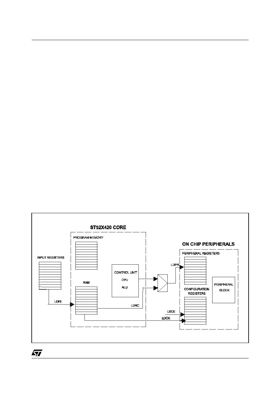
2.2 Control Unit and Data Processing Unit
The Control Unit (CU) formally includes five main
blocks. Each block decodes a set of instructions,
generating the appropriate control signals. The
main parts of the CU are illustrated in Figure 2.1.
The five different parts of the CU manage Loading,
Logic/Arithmetic, Jump, Control and the Fuzzy
instruction set.
The block called "Collector" manages the signals
deriving from the different parts of the CU, defining
the signals for the Data Processing Unit (DPU) and
the different peripherals of the microcontroller.
The block called "Arbiter" manages the different-
parts of the CU so that only one part of the system
is activated during working mode.
The CU structure is very flexible. It was designed
with the purpose of easily adapting the core of the
microcontroller to market needs. New instruction
sets or new peripherals can be easily included
without
changing
the
structure
of
the
microcontroller, maintaining code compatibility.
The CU reads the instructions stored on EPROM
(Fetch) and decodes them. According to the
instruction types, the arbiter activates one of the
main blocks of the CU. Afterwards, all the control
signals for the DPU are generated.
A set of 46 different arithmetic, fuzzy and logic
instructions is available. Each instruction requires
6 (fuzzy instructions) to 26 (DIVISION) clock
pulses to be performed.
The DPU receives, stores and sends instructions
deriving from EPROM, RAM or peripherals in order
to execute them.
2.2.1 Program Counter.
The Program Counter (PC) is a 12-bit register that
contains the address of the next memory location
to be processed by the core. This memory location
may be an opcode, operand, or an address of an
operand.
The 12-bit length allows direct addressing of a
maximum of 4,096 bytes in the program space.
After having read the current instruction address,
the PC value is incremented. The result of this
operation is shifted back into the PC.
The PC can be changed in the following ways:
s
JP (Jump)PC = Jump Address
s
InterruptPC = Interrupt Vector
s
RETIPC = Pop (stack)
s
RETPC = Pop (stack)
s
CALLPC = Subroutines address
s
ResetPC = Reset Vector
s
Normal InstructionPC = PC + 1
2.2.2 Flags.
The ST52T410/ST52x420 core includes a differ-
ent set of flags that correspond to 2 different
modes: normal mode and interrupt mode. Each
set of flags consists of a CARRY flag (C), ZERO
flag (Z) and SIGN flag (S).
One set (CN, ZN, SN) is used during normal
operation and one is used during interrupt mode
(CI, ZI, SI). Formally, the user has to manage
only one set of flags: C, Z and S.
Table 2.1 Control Signals Setting
Control
Signal
Pro-
gramming
Reset
Working
RESET
V
SS
V
SS
V
DD
TEST
V
SS
V
SS
V
SS
V
PP
12 V
V
SS
V
SS
ST52T410/ST52T420/E420
16/84
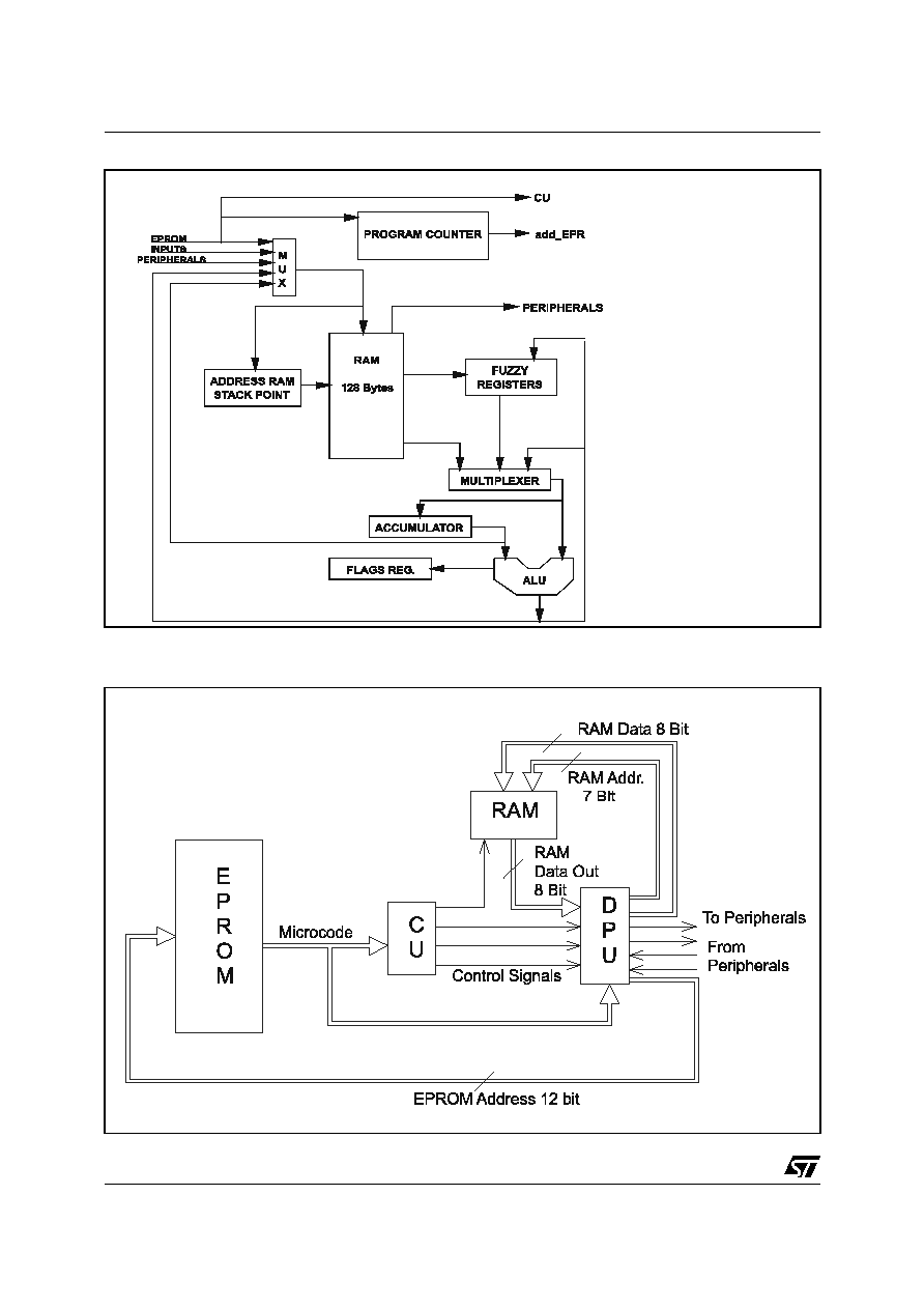
Figure 2.1 Data Processing Unit (DPU)
Figure 2.2 CU/DPU Block Diagram
ST52T410/ST52T420/E420
17/84
The ST52T410/ST52x420 core uses flags that
correspond to the actual mode. As soon as an
interrupt is generated the ST52T410/ST52x420
core uses the interrupt flags instead of the normal
flags.
Each interrupt level has its own set of flags, which
is saved in the STACK together with the Program
Counter. These flags are restored from the STACK
automatically when a RETI instruction is executed.
If the MCU was in normal mode before an interrupt,
the normal flags are restored when the RETI
instruction is executed.
Note:
A CALL subroutine is a normal mode
execution. For this reason, a RET instruction,
consequent to a CALL instruction does not affect
the normal mode set of flags.
Flags are not cleared during context switching and
remain in the state they were at the end of the last
interrupt routine switching.
The Carry flag is set when an overflow occurs
during arithmetic operations, otherwise it
is
cleared.
The Sign flag is set when an underflow occurs
during
arithmetic
operations,
otherwise
it is
cleared.
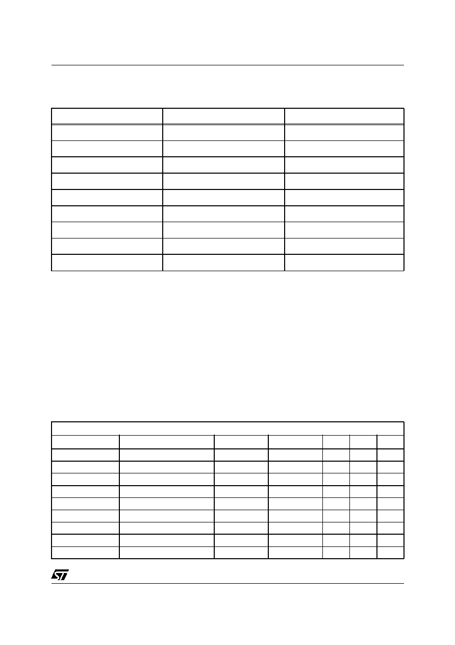
2.3 Address Spaces
ST52T410/ST52x420 has four separate address
spaces:
Figure 2.3 Address Spaces Description
s
RAM: 128 Bytes
s
Input Registers: 18 8-bit registers
s
Output Registers 9 8-bit registers
s
Configuration Registers: 17 8-bit registers
s
Program memory up to 4K Bytes
Program memory will be described in further
details in the MEMORY section
2.3.1 RAM and STACK.
RAM memory consists of 128 general purpose 8-
bit RAM registers.
All the registers in RAM can be specified by using
a decimal address. For example, 0 identifies the
first register of RAM.
To read or write RAM registers LOAD instructions
must be used. See Table 2.5
Each interrupt level has its own set of flags, which
is saved in the STACK together with the Program
Counter. These flags are restored from the STACK
automatically when a RETI instruction is executed.
When the instructions like Interrupt request or
CALL are executed, a STACK level is used to push
the PC.
The STACK is located in RAM. For each level of
stack, 2 bytes of RAM are used. The values of this
stack are stored from the last RAM register
(address 127). The maximum level of stack
must be less than 128.

ST52T410/ST52T420/E420
18/84
The STACK POINTER indicates the first level
available to store data. When a subroutine call or
interrupt request occurs, the content of the PC and
the current set of flags are stored into the level
located by the STACK POINTER.
When a interrupt return occurs (RETI instruction),
the data stored in the highest stack level is
restored back into the PC and current flags.
Instead, when a subroutine return occurs (RET
instruction) the data stored in the highest stack
level are restored in the PC not affecting the flags.
These operating modes are illustrated in Figure
2.4.
Note:
The user must pay close attention to avoid
overwriting RAM locations where the STACK could
be stored
.
2.3.2 Input Registers Bench.
The Input Registers (IR) bench consists of 18 8-bit
registers containing data or the status of the
peripherals.
All the registers can be specified by using a
decimal address (for example, 0 identifies the first
register of the IR).
The assembler instruction:
LDRI RAM_Reg. IR_i
loads the value of the i-th IR in the RAM location
identified by the
RAM_Reg
address.
The first input register is dedicated to store the
value of the stack pointer. The next 8 registers
(ADC_OUT_0:7) of the IR are dedicated to the 8
converted
values
deriving
from
the
ADC
(ST52x420 only). The last 9 Input Registers
contain data from the I/O ports and PWM/Timers.
The following table summarizes the IR address
and the relative peripherals. In order to simplify the
concept, a mnemonic name is assigned to the
registers.
The
same
name
is
used
in
VISUALSTUDIO
Æ
development tools
Figure 2.4 Stack Operation

ST52T410/ST52T420/E420
19/84
2.3.3 Configuration Registers.
The ST52T410/ST52x420 configuration Registers
allow the configuration of all the blocks of the fuzzy
microcontroller. Table 2.3 describes the functions
and the related peripherals of each of the
Configuration
Registers.
By
using
the
load
instructions, the Configuration Registers can be
set by using values stored in the Program Memory
(EPROM) or in RAM.
Use and meaning of each register will be described
in further details in the corresponding section.
Table 2.2 Input Registers
IR MNEMONIC NAME
PERIPHERAL REGISTER
ADDRESS
STACK_POINTER
STACK POINTER
0
CHAN 0 (*)
A/D CHANNEL 0 (*)
1
CHAN 1 (*)
A/D CHANNEL 1 (*)
2
CHAN 2 (*)
A/D CHANNEL 2 (*)
3
CHAN 3 (*)
A/D CHANNEL 3 (*)
4
CHAN 4 (*)
A/D CHANNEL 4 (*)
5
CHAN 5 (*)
A/D CHANNEL 5 (*)
6
CHAN 6 (*)
A/D CHANNEL 6 (*)
7
CHAN 7 (*)
A/D CHANNEL 7 (*)
8
PORT_A
PORT A INPUT REGISTER
9
PORT_B
PORT B INPUT REGISTER
10
PORT_C
PORT C INPUT REGISTER
11
PWM_ 0_COUNT
PWM/TIMER 0 COUNTER
12
PWM_ 0_ STATUS
PWM/TIMER 0 STATUS REGISTER
13
PWM_ 1_ COUNT
PWM/TIMER 1 COUNTER
14
PWM_ 1_ STATUS
PWM/TIMER 1 STATUS REGISTER
15
PWM_ 2_ COUNT
PWM/TIMER 2 COUNTER
16
PWM_ 2_ STATUS
PWM/TIMER 2 STATUS REGISTER
17
Table 2.3 Configuration Registers
CONFIGURATION REGISTER
PERIPHERAL
DESCRIPTION
REG_CONF 0
INTERRUPT MASK
Interrupts mask setting
REG_CONF 1
INTERRUPT PRIORITY
INTERRUPT PRIORITY
REG_CONF 2
WATCHDOG TIMER
Watchdog Timer Configuration
REG_CONF 3 (*)
A/D CONVERTER
A/D configuration
REG_CONF 4
PORT A
Set the relative bit like digital input
or digital output

ST52T410/ST52T420/E420
20/84
(*) ST52x420 only
2.3.4 Output Registers.
The Output Registers (OR) consist of 9 registers
containing data for the microcontroller peripherals
including the I/O Ports.
All registers can be specified by using a decimal
address (for example, 1 identifies the second OR).
By using LOAD instructions the Output Registers
(OR) may be set by using values stored in the
Program Memory (LDPE) or in RAM (LDPR)
The assembler instruction:
LDPR OR_i RAM_Reg.
loads the value of the RAM location identified by
the address RAM_Reg in the OR i-th Table 2.4
describes OR.
In order to simplify the concept, a mnemonic name
is assigned to OR. The same names are used in
VISUALFIVE
TM
5.0 development tools.
Use and meaning of each register will be described
in further details in the corresponding section.
REG_CONF 5
PWM/TIMER 0
PWM/Timer 0 Working mode
Configuration
REG_CONF 6
PWM/TIMER 0
PWM/TIMER 0 Prescaler
configuration and output waveform
selection.
REG_CONF 7
PWM/TIMER 0
PWM/TIMER 0 Working Mode
Configuration
REG_CONF 8
PWM/TIMER 1
PWM/TIMER 1 Working Mode
Configuration
REG_CONF 9
PWM/TIMER 1
PWM/TIMER 1 Prescaler
configuration and output waveform
selection.
REG_CONF 10
PWM/TIMER 2
PWM/TIMER 2 Working Mode
Configuration
REG_CONF 11
PWM/TIMER 2
PWM/Timer 2 Prescaler
configuration and output waveform
selection.
REG_CONF 12
PORT A
Set the bit 0,1 and 2 like Digital I/O
or complementary Timers Output.
REG_CONF 13
PORT B
Set the relative bit like digital input
or digital output.
REG_CONF 14
PORT B
Set the relative I/O like Digital or
Analog (*).
REG_CONF 15
PORT C
Set the relative I/O like digital input
or digital output
REG_CONF 16
PORT C
Set the relative I/O like Digital I/O
or Timers Output
Table 2.3 Configuration Registers (continued)
CONFIGURATION REGISTER
PERIPHERAL
DESCRIPTION
ST52T410/ST52T420/E420
21/84
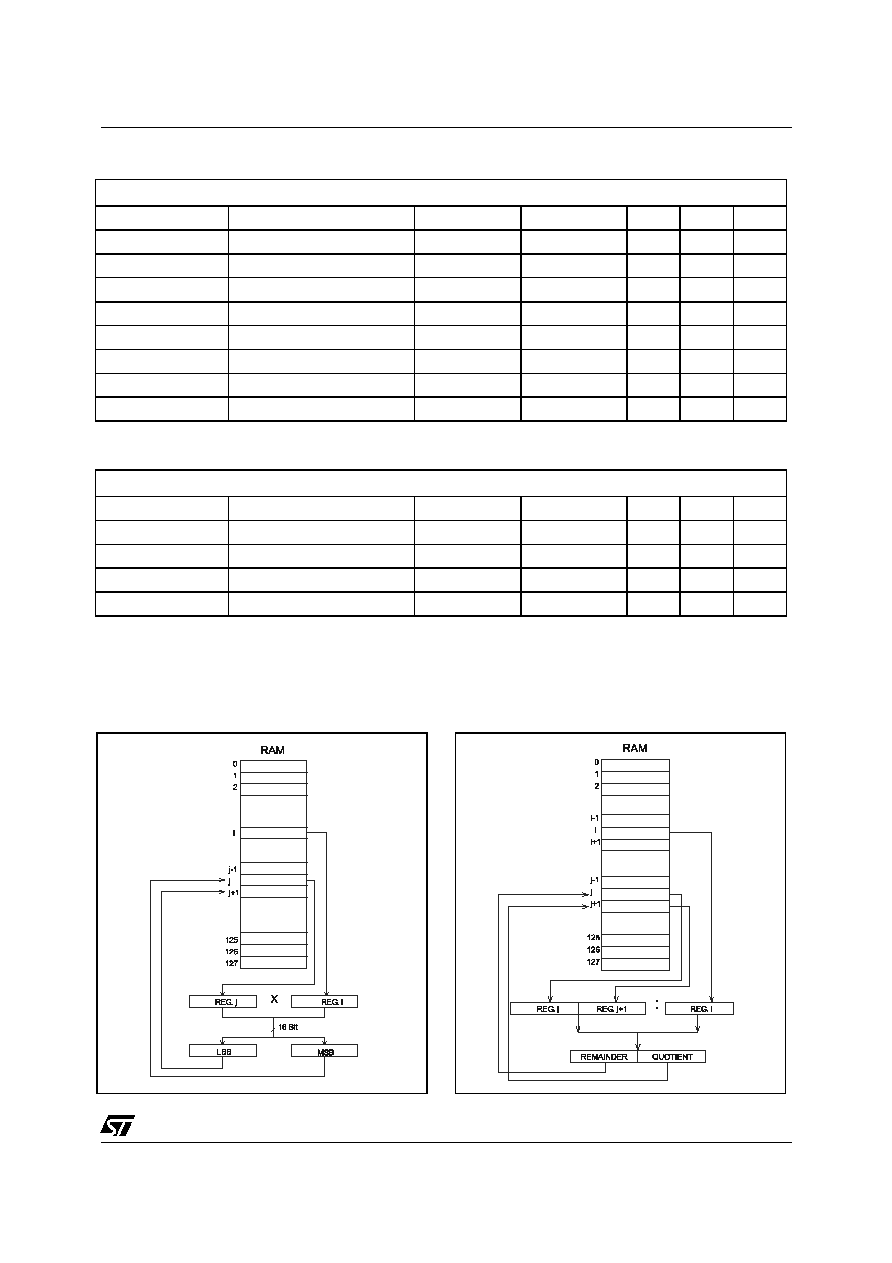
2.4 Arithmetic Logic Unit
The 8-bit Arithmetic Logic Unit (ALU) allows the
performance of arithmetic calculations and logic
instructions, which can be divided into 5 groups:
Load, Arithmetic, Jump, Interrupts and Program
Control instructions (refer to the ST52T410/
ST52x420 Assembler Set for further details).
The
computational
time
required
for
each
instruction consists of one clock pulse for each
Cycle plus 3 clock pulses for the decoding phase.
The ALU of the ST52T410/ST52x420 can perform
multiplication
(MULT)
and
division
(DIV).
Multiplication is performed by using 8 bit operands
storing the result in 2 registers (16 bit values), see
Figure 2.5 and Figure 2.6.
WARNING 1: The current page register value
set with the PGSET instruction is lost after a
jump, call, or an interrupt jump.
WARNING 2: If the LSB of the multiplication
result is 0, the Zero flag is set although the
result is not 0.
Table 2.4 Output Registers
OR MNEMONIC NAME
PERIPHERAL REGISTER
ADDRESS
PORT_ A
PORT A OR
0
PORT_ B
PORT B OR
1
PORT_C
PORT C OR
2
PWM_0_COUNT
TIMER/PWM 0 COUNTER
3
PWM_0_RELOAD
TIMER/PWM 0 RELOAD REGISTER
4
PWM_1_COUNT
TIMER/PWM 1 COUNTER
5
PWM_1_RELOAD
TIMER/PWM 1 RELOAD REGISTER
6
PWM_ 2_ COUNT
TIMER/PWM 2 COUNTER
7
PWM_2_RELOAD
TIMER/PWM 2 RELOAD REGISTER
8
Table 2.5 Load instructions
Load Instructions
Mnemonic
Instruction
Bytes
Cycles
Z
S
C
LDCE
LDCE conf, EPROM
3
17
-
-
-
LDCR
LDCR conf, RAM
3
14
-
-
-
LDFR
LDFR FUZZY_i_RAM RAM
3
14
-
-
-
LDPE
LDPE per, EPROM
3
17
-
-
-
LDPE
LDPE per, (RAM)
3
17
-
-
-
LDPR
LDPR reg, RAM
3
14
-
-
-
LDRC
LDRC RAM, const
3
14
-
-
-
LDRE
LDRE RAMi, EPROMi
3
16
-
-
-
LDRE
LDRE (RAMi), (RAMj)
3
18
-
-
-
ST52T410/ST52T420/E420
22/84
LDRI
LDRI RAM, inp_reg
3
15
-
-
-
LDRR
LDRR RAMi, RAMj
3
16
-
-
-
PGSET
PGSET const
2
9
-
-
-
Table 2.6 Arithmetic & Logic instructions set
Arithmetic Instructions
Mnemonic
Instruction
Bytes
Cycles
Z
S
C
ADD
ADD regi, regj
3
17
I
-
I
ADDO
ADDO regi, regj
3
20
I
I
I
AND
AND regi, regj
3
17
I
-
-
ASL
ASL regi
2
15
I
-
I
ASR
ASR regi
2
15
I
I
-
DEC
DEC regi
2
15
I
I
-
DIV
DIV regi, regj
3
26
I
I
I
INC
INC regi
2
15
I
-
I
MULT
MULT regi, regj
3
19
I
-
-
NOT
NOT regi
2
15
I
-
-
OR
OR regi, regj
3
17
I
-
-
SUB
SUB regi, regj
3
17
I
I
-
SUBO
SUBO regi, regj
3
20
I
I
I
MIRROR
MIRROR regi
2
15
I
-
-
Table 2.7 Jump Instruction Set
Jump instructions
mnemonic
instruction
bytes
cycles
z
s
c
CALL
CALL addr
3
18
-
-
-
JP
JP addr
3
12
-
-
-
JPC
JPC addr
3
10/12
-
-
-
JPNC
JPNC addr
3
10/12
-
-
-
JPNS
JPNS addr
3
10/12
-
-
-
JPNZ
JPNZ addr
3
10/12
-
-
-
JPS
JPS addr
3
10/12
-
-
-
JPZ
JPZ addr
3
10/12
-
-
-
RET
RET
1
13
-
-
-
Table 2.5 Load instructions
ST52T410/ST52T420/E420
23/84
Notes:
I affected
- not affected
Figure 2.5 Multiplication
Figure 2.6 Division
Table 2.8 Interrupt Instructions Set
Interrupt Instructions
Mnemonic
Instruction
Bytes
Cycles
Z
S
C
HALT
HALT
1
7/15
-
-
-
MEGI
MEGI
1
7/15
-
-
-
MDGI
MDGI
1
6
-
-
-
RETI
RETI
1
12
-
-
-
RINT
RINT INT
2
8
-
-
-
UDGI
UDGI
1
6
-
-
-
UEGI
UEGI
1
7/15
-
-
-
WAITI
WAITI
1
7/14
-
-
-
Table 2.9 Control Instructions Set
Control Instructions
Mnemonic
Instruction
Bytes
Cycles
Z
S
C
FUZZY
FUZZY
1
5
-
-
-
NOP
NOP
1
6
-
-
-
WDTRFR
WDTRFR
1
7
-
-
-
WDTSLP
WDTSLP
1
6
-
-
-
ST52T410/ST52T420/E430
24/84
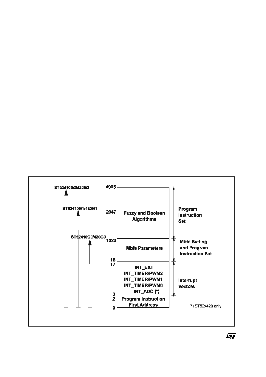
3 EPROM
EPROM memory provides an on-chip user-
programmable non-volatile memory, which allows
fast and reliable storage of user data.
EPROM memory can be locked by the user. In
fact, a memory location called Lock Cell is devoted
to lock EPROM and avoid external operations. A
software identification code, called ID CODE,
distinguishes which software version is stored in
the memory.
32 kbits of memory space with an 8-bit internal
parallelism (up to 4 kbytes) addressed by a 12-bit
bus are available. The data bus is 8 bits.
Memory has a double supply: V
PP
is equal to
12V
±
5% in Programming Phase or to V
SS
during
Working Phase. V
DD
is equal to 5V
±
10%.
ST52T410/ST52x420 EPROM memory is divided
into three main blocks (see Figure ):
s
Interrupt Vectors memory block
(3 through 17)
contains the addresses for the interrupt routines.
Each address is composed of three bytes.
Figure 3.1 Program Memory Organization
s
Mbfs Setting memory block
(18 through
MemAdd
) contains the coordinates of the
vertexes of every Mbf defined in the program.
s
The maximum value of MemAdd is 1023. This
area is dynamically assigned according to the
size of the fuzzy routines. The unused memory
area, if any, is assigned to the Program
Instruction Set memory block.
s
The Program Instructions Set memory block
(MemAdd through 4095) contains the instruction
set of the user program.
Locations 0, 1 and 2 contain the address of the first
microcode instruction.The operations that can be
performed on EPROM during the Programming
Phase are: Stand By, Memory Writing, Reading
and Verify/Margin Mode, Memory Lock, IDCode
Writing and Verify.

ST52T410/ST52T420/E430
25/84
Figure 3.2 Eprom Programming Timing
The operations above are managed by using the
internal 4-bit EPROM Control Register. The
reading phase is executed with V
PP
= 5V
±
5%, while
the
verify/Margin
Mode
phase
needs
V
PP
=
12V
±
5%. The Blank Check must be a reading
operation with V
PP
= 5V
±
5%.
Table 3.1 illustrates EPROM Control Register
codes used to identify the operation running.
3.1 EPROM Programming Phase Procedure
The Programming mode is selected by applying
12V
±
5% voltage or 5V
±
5% voltage to the V
PP
pin
and setting the control signal as following:
RESET =Vss
TEST =Vss
If the V
PP
voltage is 5V
±
5% only reading may be
performed.
RST_ADD, INC_ADD, RST_CONF, INC_CONF
and PHASE are the control signals used during the
Programming Mode.
PHASE, RST_CONF and RST_ADD signals are
active on level, the others are active on rising
edge.
Table 3.1 EPROM Control Register
OPERATION
REGISTER VALUE
Stand By
0
Memory Reading/Verify
1
Memory Unlock and
Lock Status Reading
2
Memory Writing
3
Memory Lock
4
ID CODE Writing
5
Memory Lock Status
Reading/Verify
9
ID CODE Reading/
Verify
10
MEMORY UNLOCK
MEMORY WRITING
LOCATION ADDRESS =1
DATA
IN
MEMORY VERIFY
MARGIN MODE
DATA
OUT
VALID
DATA
VALID
DATA
VALID
DATA
DATA
OUT
DATA
OUT
100nS
10
µ
S
PA(0:7)
RST_ADD
RST_CONF
INC_ADD
INC_CONF
PHASE

ST52T410/ST52T420/E430
26/84
PHASE and RST_ADD signals are active low,
RST_CONF signal is active high.
Port A is used for the memory data I/O.
(See Table
3.1 for pin reference on the different packages)
.
Memory may be locked by means of the Memory
Lock Status, which is a flag used to enable
EPROM operations.
If Memory Lock Status is 1 all EPROM operations
are enabled, otherwise the user may only read
(and verify) the OTP code and the Memory Lock
Status.
Only if EPROM is not locked by means of Lock Cell
(see EPROM Locking may EPROM operations be
enabled by changing the Memory Lock Status from
0 to 1.
RST_ADD signal resets the memory address
register and the Memory Lock Status. When the
RST_ADD becomes high, the memory must be
unlocked in order to read or write.
INC_ADD signal increments the memory address.
RST_CONF signal resets the EPROM Control
Register. When RST_CONF is high, the DATA I/
O Port A is in output, otherwise it is always in
input.
INC_CONF signal increments the EPROM Control
Register value.
PHASE signal validates the operation selected by
means of the EPROM Control Register value.
3.1.1 EPROM Operation.
In order to execute an EPROM operation (See
Table 3.1), the corresponding identification value
must be loaded in the EPROM Control Register.
The signal timing is the following: RST_ADD= high
and PHASE= high, RST_CONF changes from low
to high level, to reset the EPROM Control Register,
and INC_CONF signal generates a number of
positive pulses equal to the value to be loaded.
After this sequence, a negative pulse of the
PHASE signal will validate the operation selected.
The minimum PHASE signal pulse width must be
10
µ
s for EPROM Writing Operation and 100 ns for
the others.
When RST_CONF is high, DATA I/O Port A is
enabled
in
output
and
the
reading/verifying
operation results are available.
After a writing operation, when RST_CONF is high,
Port A is in output without valid data.
3.1.2 EPROM Locking.
The Memory Lock operation, which is identified
with the number 4 in the EPROM Control Register,
writes "0" in the Memory Lock Cell.
At the beginning of an External Operation, when
the RST_ADD signal changes from low level to
high level, the Memory Lock Status is "0", therefore
it must be unlocked before proceeding.
In order to unlock the Memory Lock Status the
operation, which is identified by the number 2 in
the EPROM Control Register must be executed
(see Figure 3.2).
Memory Lock Status can be changed only if
Memory Lock Cell is "1". After a Memory Lock
operation external operations cannot be executed
except to read (or verify) the OTP Code and the
Memory Lock Status.
3.1.3 EPROM Writing.
When the memory is blank, all bits are at logic level
"1". Data is introduced by programming only the
zeros in the desired memory location. However, all
input data must contain both "1" and "0".
The only way to change "0" into "1" is to erase the
entire memory (by exposure to Ultra Violet light)
and reprogram it.
The memory is in Writing mode when the EPROM
Control Register value is 3.
The V
PP
voltage must be 12V
±
5%, with stable data
on the data bus PA(0:7).
The timing signals are the following (see Figure ):
1) RST_ADD and RST_CONF change from low to
high level,
2) two pulses on INC_CONF signal load the
Memory Unlock operation code,
3) a negative pulse (100 ns) on the PHASE signal
validates the Memory Unlock operation,
4) a negative pulse on RST_CONF signal resets
the EPROM Control Register,
5) three positive pulses on INC_CONF load the
Memory Writing operation code,
6) a train of positive pulses on INC_ADD signal
increments the memory location address up to the
requested value (generally this is a sequential
operation and only one pulse is used),
7) a negative pulse (10
µ
s) on the PHASE signal
validates the Memory Writing operation.

ST52T410/ST52T420/E430
27/84
3.1.4 EPROM Read/Verify Margin Mode.
The read phase is executed with V
PP
= 5V
±
5%,
instead of the verify phase that needs V
PP
=
12V
±
5%.
The Memory Verify operation is available in order
to verify the accuracy of the data written. A
Memory Verify Margin Mode operation can be
executed immediately after writing each byte, in
this case (see Figure 3.2):
1) a positive pulse on RST_CONF signal resets the
EPROM Control Register, if it wasn't already reset;
2) one positive pulse on INC_CONF loads the
Memory Read/Verify operation code;
3) a negative pulse (100 ns) on the PHASE signal
validates the Memory Reading / Verify operation;
4) a negative pulse on RST_CONF signal puts in
the PA(0:7) port the value stored in the actual
memory address and resets the EPROM Control
Register;
If an error occurred writing, the user has to repeat
EPROM writing.
3.1.5 Stand by Mode.
EPROM has a standby mode, which reduces the
active current from 10mA (Programming mode) to
less than 100
µ
A. Memory is placed in standby
mode by setting the PHASE signal at a high level
or when the EPROM Control Register value is 0
and the PHASE signal is low.
3.1.6 ID code.
A software identification code, called ID code may
be written in order to distinguish which software
version is stored in the memory.
64 Bytes are dedicated to store this code by using
the address values from 0 to 63.
The ID Code may be read or verified even if the
Memory Lock Status is "0".
The timing signals are the same as that of a normal
operation.
3.2 Eprom Erasure
The
transparent
window
available
in
the
CSDIP32W package, allows the memory contents
to be erased by exposure to UV light.
Erasure begins when the device is exposed to light
with a wavelength shorter than 4000≈. Sunlight, as
well as some types of artificial light, includes
wavelengths in the 3000-4000≈ range which, on
prolonged exposure can cause erasure of memory
contents. Therefore, it is recommended that
EPROM devices be fitted with an opaque label
over the window area in order to prevent
unintentional erasure.
The erasure procedure recommended for EPROM
devices consists of exposure to short wave UV
light having a wavelength of 2537≈. The minimum
integrated dose recommended (intensity x expo-
sure time) for complete erasure is 15Wsec/cm 2.
This is equivalent to an erasure time of 15-20
minutes using a UV source having an intensity of
12mW/cm 2 at a distance of 25mm (1 inch) from
the device window.
ST52T410/ST52T420/E420
28/84
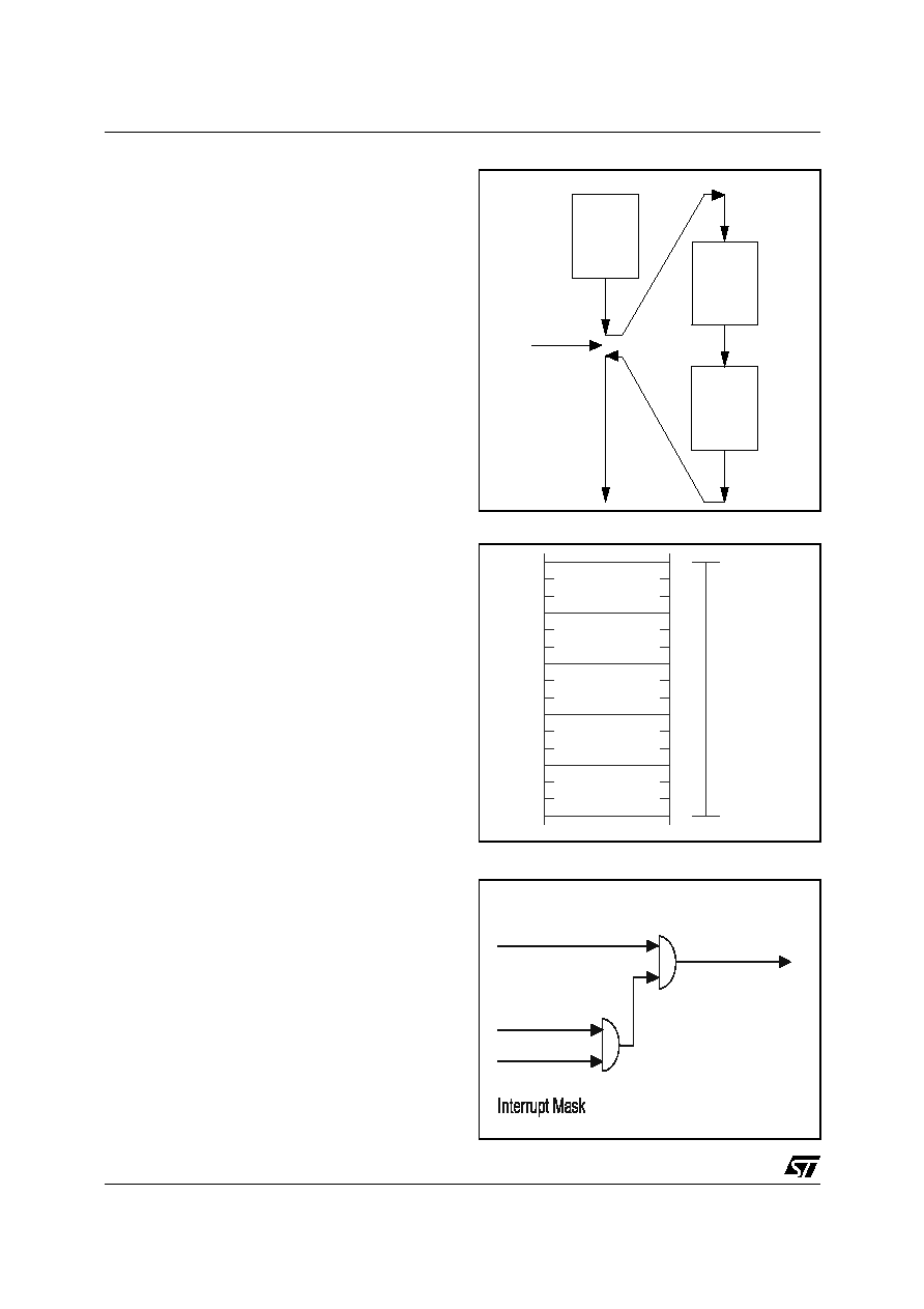
4 INTERRUPTS
The Control Unit (CU) responds to peripheral
events and external events via its interrupt
channels.
When such an events occur, if the related interrupt
is not masked and according to a priority order, the
current program execution can be suspended to
allow the CU to execute a specific response
routine.
Each interrupt is associated with an interrupt
vector that contains the memory address of the
related interrupt service routine. Each vector is
located in the Program Space (EPROM Memory)
at a fixed address (see Interrupt Vectors Table
4.2).
4.1 Interrupt Operation
If there are pending interrupts at the end of an
arithmetic or logic instruction, the one with the
highest priority is passed. Passing an interrupt
means storing the arithmetic flags and the current
PC in the stack and executing the associated
Interrupt routine, whose address is located in three
bytes of the EPROM memory location between
address 2 and 17.
The Interrupt routine is performed as a normal
code, checking if a higher priority interrupt has to
be passed at the end of each instruction. An
Interrupt request with the higher priority stops the
lower priority Interrupt. The Program Counter and
the arithmetic flags are stored in the stack.
With the RETI (Return from Interrupt) instruction
the arithmetic flags and Program Counter (PC) are
restored from the top of the stack. This stack was
already described in section RAM and STACK.
An Interrupt request cannot stop processing of the
fuzzy rule, but this is passed only after the end of a
fuzzy rule or at the end of a logic, or arithmetic
instruction.
NOTE: A fuzzy routine can only be interrupted
in the Main program. An interrupt request
cannot stop a Fuzzy function that is running
inside another interrupt routine. In order to use
a Fuzzy function inside an interrupt routine, the
user MUST include the Fuzzy function between
an UDGI (MDGI) instruction and an UEGI
(MEGI)
instruction
(see
the
following
paragraphs), so that the interrupt request may
be disabled during the execution of the fuzzy
function.
4.2 Global Interrupt Request Enabling
When an Interrupt occurs, it generates a Global
Interrupt Pending (GIP), that can be masked by
software. After a GIP a Global Interrupt Request
(GIR) will be generated and Interrupt service
Figure 4.1 Interrupt Flow
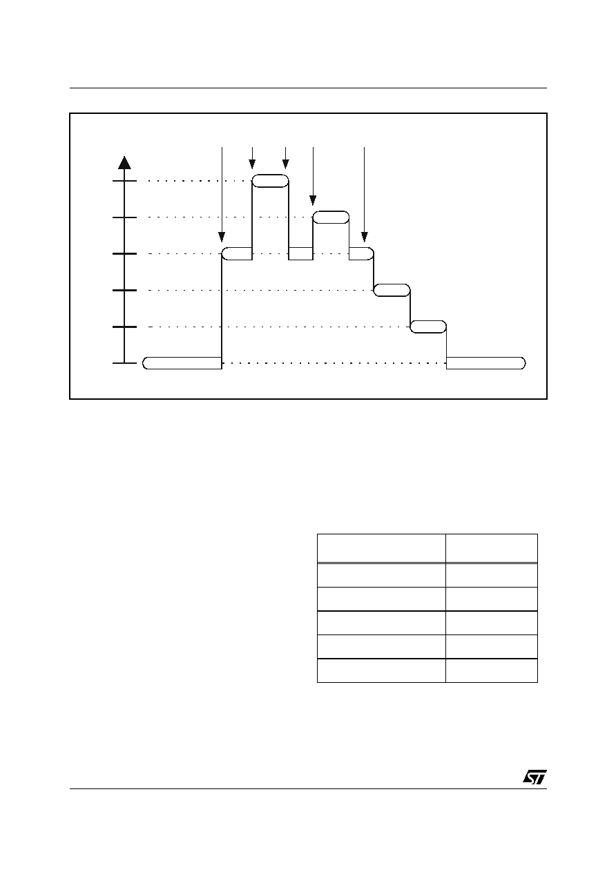
Figure 4.2 Interrupt Vectors mapping
Figure 4.3 Global Interrupt Request generation
NORMAL
PROGRAM
FLOW
INTERRUPT
SERVICE
ROUTINE
RETI
INSTRUCTION
INTERRUPT
INT_EXT
INT_ADC
INT_PWM/
0
TIMER
INT_PWM/
1
TIMER
INT_PWM/
2
TIMER
3
4
5
6
7
8
9
10
11
12
13
14
15
16
17
INTERRUPT
VECTORS
Global Interrupt
Pending
User Global
Interrupt Mask
Macro Global
Global Interrupt
Request

ST52T410/ST52T420/E420
29/84
Routine associated to the interrupt with higher
priority will start.
In order to avoid possible conflicts between
interrupt masking set in the main program, or
inside high level language compiler macros, the
GIP is hung up through the User Global Interrupt
Mask or the Macro Global Interrupt Mask (see
Figure 4.2).
UEGI/UDGI instruction switches on/off the User
Global Interrupt Mask, enabling/disabling the GIR
for the main program.
MEGI/MDGI instructions switch the Macro Global
Interrupt Mask on/off, in order to ensure that the
macro will not be broken.
4.3 Interrupt Sources
ST52T410/ST52x420 manages interrupt signals
generated by the internal peripherals (PWM/
Timers and Analog to Digital Converter) or coming
from the INT/PC0 pin. The External Interrupt is
active on the rising of INT/PC0 signal.
Each peripheral can be programmed in order to
generate the associated interrupt; further details
are described in the related chapter.
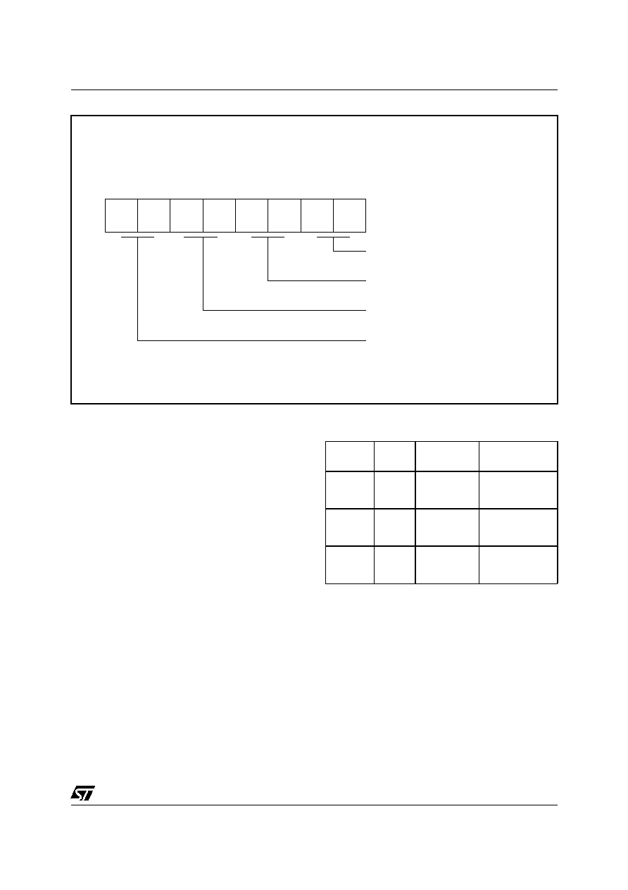
4.4 Interrupt Maskability
The interrupts can be masked by configuring the
REG_CONF 0 by means of LDCR, or LDCE,
instruction. The interrupt is enabled when the bit
associated to the mask interrupt is "1". Viceversa,
when the bit is "0", the interrupt is masked and is
kept pendent.
For example:
LDRC 10,6 //load the constant 6 in the
RAM Register 10
LDCR 0, 10 // set the CONF_REG 0 with
the value stored in the RAM Register
10
the result is CONF_REG0 =00000110 enabling the
interrupts deriving from the ADC (INT_ADC)
(ST52x420 only) and from the PWM/TIMER 0
(INT_PWM/TIMER0).
(*) ST52x420 only
Reset Configuration `000000'
Table 4.1 Configuration Register 0
Description
Bit
Name
Value
Description
0
MSKE
0
External Interrupt
Masked
1
External Interrupt
Not Masked
1
MSKAD
0
A/D Converter (*)
Interrupt
Masked
1
A/D Converter (*)
Interrupt
Not Masked
2
MSKTM0
0
PWM/TIMER 0
Interrupt
Masked
1
PWM/TIMER 0
Interrupt
Not Masked
3
MSKTM1
0
PWM/TIMER 1
Interrupt
Masked
1
PWM/TIMER 1
Interrupt
Not Masked
4
MSKTM2
0
PWM/TIMER 2
Interrupt
Masked
1
PWM/TIMER 2
Interrupt
Not Masked
5
Not used
-
6
Not used
4
Not used
-

ST52T410/ST52T420/E420
30/84
(*) ST52x420 only
Figure 4.4 Interrupt Configuration Register 0
Table 4.2
Interrupts Description
Name
Description
Priority
Peripheral
Code
Maskable
EPROM
Locations
INT_ADC (*)
ADC
Int
Programmable
00
yes
3-5
INT_PWM/
TIMER0
PWM/TIMER 0
Int
Programmable
01
yes
6-8
INT_PWM/
TIMER1
PWM/TIMER 1
Int
Programmable
10
yes
9-11
INT_PWM/
TIMER2
PWM/TIMER 2
Int
Programmable
11
yes
12-14
INT_EXT
External
Interrupt (INT)
Ext
Highest
-
yes
15-17
7
0
MSKTM0 MSKAD MSKE
REG_CONF 0
EXTERNAL INT.
A/D CONV. INT.
PWM/TIMER 0 INT.
PWM/TIMER 1 INT.
PWM/TIMER 2 INT.
NOT USED
MSKTM1
MSKTM2
not used not used
not used
ST52T410/ST52T420/E420
31/84
Figure 4.5 Interrupt Configuration Register 1
4.5 Interrupt Priority
Six priority levels are available: level 5 has the
lowest priority, level 0 has the highest priority.
Level 5 is associated to the Main Program, levels 4
to 1 are programmable by means of the priority
registers called REG_CONF1 (see Figure 4.5 and
Table 4.3); whereas the higher level is related to
the external interrupt (INT_EXT).
PWM/Timers and ADC are identified by a two-bit
Peripheral Codes (see Table 4.2); in order to set
the
i
-th priority level the user must write the
peripheral label
i
in the related INT
i
priority level.
i.e.
LDRC
10,
201
//(load
the
value
201='11001001' in the RAM Register 10)
LDCR
1,
10
//
set
the
REG_CONF1=
`11001001'
The following priority levels are defined:
s
Level 1: INT_PWM/TIMER0 (PWM/TIMER 0
Code: 01)
s
Level 2: INT_PWM/TIMER0 (PWM/TIMER 1
Code: 10)
s
Level 3: INT_ADC (ADC Code: 00) (ST52x420
only)
s
Level 4: INT_PWM/TIMER0 (PWM/TIMER 2
Code: 11)
Table 4.3 Conf. Register 1
Bit
Name
Value
Level
0, 1
INT1
Peripheral
Code
High
2,3
INT2
Peripheral
Code
Medium-High
4,5
INT3
Peripheral
Code
Medium-Low
7
0
REG_CONF 1
PRIORITY HIGH
PRIORITY MED. HIGH
PRIORITY MED. LOW
PRIORITY LOW
LOW
LOW
MEDL
MEDL
MEDH
HIGH
HIGH
MEDH
ST52T410/ST52T420/E420
32/84
Figure 4.6 Example of a sequence of Interrupt requests
Note: The Interrupt priority must be fixed at the
beginning of the main program because at the
RESET
REG_CONF1='00000000'
it
could
generate
erroneous
operations.
During
program execution the interrupt priority can
only be modified with the following procedure:
STEP 1:
Mask the interrupts by means of a UDGI (or
MDGI) instruction
STEP 2:
Change the REG_CONF 1 values to modify the
interrupt priority
STEP 3:
Reset all the pending interrupt instructions by
means of RINT instructions.
STEP 4:
Unmask the interrupts by means of a UEGI (or
MEGI) instruction
When a source provides an Interrupt request and
the request processing is also enabled, the CU
changes the normal sequential flow of a program
by transferring program control to a selected
service routine.
When an interrupt occurs the CU executes a JUMP
instruction to the address loaded in the related
location of the Interrupt Vector.
When the execution returns to the original program
it immediately begins following the instruction that
was interrupted.
(*) ST52x420 only
Table 4.4 RINT Instruction code
Peripheral Name
Value
INT_ADC (*)
0
PWM/TIMER 0
1
PWM/TIMER 1
2
PWM/TIMER 2
3
INT_EXT
4
MAIN PROGRAM
5
4
3
2
1
0
PRI2
PRI0
PRI2
PRI1
PRI2
PRI3
PRI4
MAIN PROGRAM
PRIORITY
LEVEL
PRI2
PRI0
PRI4
PRI1
PRI3

ST52T410/ST52T420/E420
33/84
4.6 Interrupts and Low power mode
All interrupts allow the processor to leave the WAIT
low power mode. Only the external Interrupt allows
the processor to leave the HALT low power mode.
4.7 Interrupt RESET
An eventually pending interrupt can be reset with
the instruction
RINT j
, which resets the interrupt
j
-th where
j
identifies the peripherals as described
in the following table (see Table 4.4).
The assembler instruction:
RINT 2
Resets the PWM/Timer 1 interrupt.
Note: The RINT command must be preceded
from a UDGI (or MDGI) command and followed
by a UEGI (or MEGI) command.
WARNING: If an interrupt is reset, with the RINT
instruction within its own interrupt routine, the
priority level of the interrupt becomes the
lowest and the routine can be immediately
interrupted
by
a
lower
priority
interrupt
request.
ST52T410/ST52T420/E420
34/84
5 CLOCK, RESET & POWER SAVING MODE
5.1 System Clock
The
ST52T410/ST52x420
Clock
Generator
module generates the internal clock for the internal
Control Unit, ALU and on-chip peripherals and it is
designed to require a minimum number of external
components.
The
ST52T410/ST52x420
oscillator
circuit
generates an internal clock signal with the same
period and phase as that of the OSCin input pin.
The maximum frequency allowed is 20 Mhz.
The system clock may be generated by using
either a quartz crystal, ceramic resonator or an
external clock.
The different methods of the clock generator are
illustrated in Figure 5.1.
When an external clock is used, it must be
connected on the OSCin pin, while OSCout can be
floating.
The crystal oscillator start-up time is a function of
many variables: crystal parameters (especially
R
s
),
oscillator
load
capacitance
(CL),
IC
parameters,
environment
temperature,
supply
voltage.
Figure 5.1 Oscillator Connections
Note: The crystal or ceramic leads and circuit
connections must be as short as possible. Typical
values for CL1, CL2 are 10pF for a 20 MHz crystal.
5.2 RESET
There are two Reset sources:
- RESET pin (external source.)
- WATCHDOG (internal source)
When a Reset event happens, the user program
restarts from the beginning.
The Reset pin is an input. An internal reset does
not affect this pin.
A Reset signal originated by external sources is
recognized instantaneously. The RESET pin may
be used to ensure V
DD
has risen to a point where
the MCU can operate correctly before the user
program runs. In working mode Reset must be set
to `1' (see Table 2.1).
5.3 Power Saving Mode
There are two Power Saving modes: WAIT and
HALT mode. These conditions may be entered
using the WAIT or HALT instructions.
5.3.1 Wait Mode
Wait mode places the MCU in low power
consumption by stopping the CPU. All peripherals
OSCin
OSCout
ST52X420
OSCin
ST52X420
OSCout
CRYSTAL CLOCK
EXTERNAL CLOCK
Cl1
10pF
Cl2
10pF
CLOCK
INPUT
FLOATING

ST52T410/ST52T420/E420
35/84
and the watchdog remain active. During WAIT
mode, Interrupts are enabled. The MCU will
remain in Wait mode until an Interrupt or a RESET
occurs, whereupon the Program Counter jumps to
the interrupt service routine or, if a RESET occurs,
at the beginning of the user program.
REMARK: In Wait mode the CPU clock does not
stop.
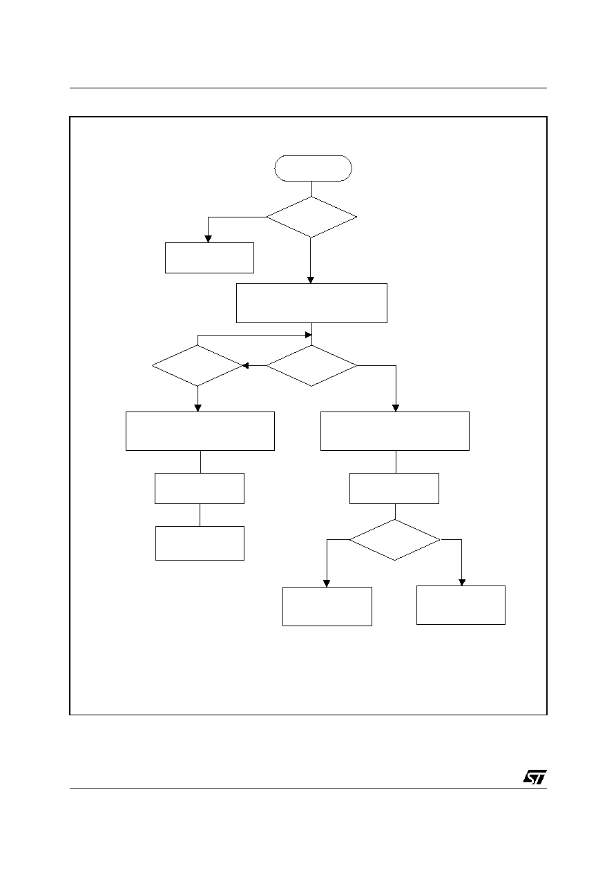
5.3.2 Halt Mode
Halt mode is MCU's lowest power consumption
mode, which is entered by executing the HALT
instruction. The internal oscillator is turned off,
causing all internal processing to stop, including
the operations of the on-chip peripherals.
Figure 5.2 Reset Block Diagram
Figure 5.3 Simple Reset Circuit
Halt mode cannot be used when the watchdog
is enabled.
If the HALT instruction is executed while the
watchdog system is enabled, it will be skipped
without modifying the normal CPU operations.
The ICU can exit Halt mode after an external inter-
rupt or reset. The oscillator is then turned on and
stabilization time is provided before restarting
CPU operations. Stabilization time is 4096 CPU
clock cycles after the interrupt and 1.000.000 after
the Reset.
After the start up delay, the CPU restarts opera-
tions by serving the external interrupt routine.
Reset makes the ICU exit from HALT mode and
restart, after the delay, from the beginning of the
user program after the delay.
Warning: if the External Interrupt is disabled, the
ICU exits from the Halt mode and jumps to the
lower priority interrupt routine.
Figure 5.4 WAIT Flow Chart
WATCHDOG RESET
RESET
INTERNAL
RESET
Vcc
100
F
10k
2.2k
2.2k
1 F
RESET
ST52T410/ST52T420/E420
36/84
HALT INSTRUCTION
WATCHDOG
ENABLED
HALT INSTRUCTION
SKIPPED
YES
NO
OSCILLATOR
OFF
PERIPHERALS CLOCK
OFF
CPU CLOCK
OFF
YES
4096 CPU CLOCK
CYCLES DELAY
RESTART PROGRAM
SERVICING THE
EXTERNAL
INTERRUPT ROUTINE
EXTERNAL
INTERRUPT
NO
YES
NO
EXTERNAL
INTERRUPT
ENABLED
RESTART PROGRAM
SERVICING THE
LOWER PRIORITY
INTERRUPT ROUTINE
YES
NO
RESET
RESET CPU
AND RESTART
USER PROGRAM
OSCILLATOR
ON
PERIPHERALS CLOCK
ON
CPU CLOCK
ON
1000000 CPU CLOCK
CYCLES DELAY
OSCILLATOR
ON
PERIPHERALS CLOCK
ON
CPU CLOCK
ON
Figure 5.5 HALT Flow Chart

ST52T410/T420/E420
37/84
6 FUZZY COMPUTATION (DP)
The ST52T410/ST52x420 Decision Processor
(DP) main features are:
s
Up to 8 Inputs with 8-bit resolution;
s
1 Kbyte of Program/Data Memory available to
store more than 300 to Membership Functions
(Mbfs) for each Input;
s
Up to 128 Outputs with 8-bit resolution;
s
Possibility of processing fuzzy rules with an
UNLIMITED number of antecedents;
s
UNLIMITED number of Rules and Fuzzy Blocks.
The limits on the number of Fuzzy Rules and
Fuzzy program blocks are only related to the
Program/Data Memory size.
6.1 Fuzzy Inference
The block diagram shown in Figure 6.1 describes
the different steps performed during a Fuzzy
algorithm. The ST52T410/ST52x420 Core allows
for the implementation of a Mamdani type fuzzy
inference with crisp consequents. Inputs for fuzzy
inference are stored in 8 dedicated Fuzzy input
registers. The LDFR instruction is used to set the
Input Fuzzy registers with values stored in the
Register File. The result of a Fuzzy inference is
stored directly in a location of the Register File.
6.2 Fuzzyfication Phase
In this phase the intersection (alpha weight)
between the input values and the related Mbfs
(Figure 6.2) is performed.
Eight Fuzzy Input registers are available for Fuzzy
inferences.
Figure 6.1 Fuzzy Inference
Figure 6.2 Alpha Weight Calculation
After loading the input values by using the LDFR
assembler instruction, the user can start the fuzzy
inference
by
using
the
FUZZY
assembler
instruction. During fuzzyfication: input data is
transformed in the activation level (alpha weight) of
the Mbf's.
6.3 Inference Phase
The Inference Phase manages the alpha weights
obtained during the fuzzyfication phase to compute
the truth value (
) for each rule.
This is a calculation of the maximum (for the OR
operator) and/or minimum (for the AND operator)
performed on alpha values according to the logical
connectives of Fuzzy Rules.
Several conditions may be linked together by
linguistic connectives AND/OR, NOT operators
and brackets.
The truth value
and the related output singleton
are used by the Defuzzyfication phase, in order
to complete the inference calculation.
11
1m
n1
nm
FUZZYFICATION
INFERENCE
PHASE
DEFUZZYFICATION
N rules
N rules -1
2
1
Input Values
Output Values
1
ij
j-th Mbf
i-th INPUT VARIABLE
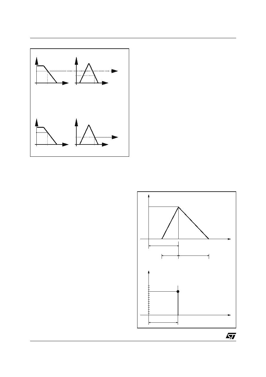
ST52T410/T420/E420
38/84
Figure 6.3 Fuzzyfication
6.4 Defuzzyfication
In
this
phase
the
output crisp
values
are
determined by implementing the consequent part
of the rules.
Each consequent Singleton X
i
is multiplied by its
weight values
i
, calculated by the Decision
processor, in order to compute the upper part of
the Defuzzyfication formula.
Each output value is obtained from the consequent
crisp values (X
i
) by carrying out the following
Defuzzyfication formula:
where:
i = identifies the current output variable
N = number of the active rules on the current
output
ij
= weight of the j-th singleton
X
ij
= abscissa of the j-th singleton
The Decision Processor outputs are stored in the
RAM location i-th specified in the assembler
instruction OUT i.
6.5 Input Membership Function
The Decision Processor allows the management of
triangular Mbfs. In order to define an Mbf, three
different parameters must be stored on the
Program/Data Memory (see Figure 6.4):
s
the vertex of the Mbf: V;
s
the length of the left semi-base: LVD;
s
the length of the right semi-base: RVD;
In order to reduce the size of the memory area and
the computational effort the vertical range of the
vertex is fixed between 0 and 15 (4 bits)
By using the previous memorization method
different kinds of triangular Membership Functions
may be stored. Figure 6.5 shows some examples
of valid Mbfs that can be defined in ST52T410/
ST52x420.
Each Mbf is then defined storing 3 bytes in the first
Kbyte of the Program/Data Memory.
The Mbf is stored by using the following instruction:
MBF
n_mbf lvd v rvd
where:
n_mbf
is a tag number that identifies the Mbf
lvd
,
v
, and
rvd
are the parameters that describe the
Mbf's shape as described above.
Figure 6.4 Mbfs Parameters
Input 1
X1
1
Input 2
X2
2
OR = Max
IF INPUT 1 IS X1 OR INPUT 2 IS X2 THEN .......
Input 1
X1
1
Input 2
X2
2
IF INPUT 1 IS X1 AND INPUT 2 IS X2 THEN .......
Y
i
X
ij
ij
j
N
ij
j
N
---------------------
=
X
15
LVD
RVD
V
15
0
0
Input Mbf
Output Singleton
Output Variable
Input Variable
w

ST52T410/T420/E420
39/84
Figure 6.5 Example of valid Mbfs
6.6 Output Singleton
The Decision Processor uses a particular kind of
membership function called Singleton for its output
variables. A Singleton doesn't have a shape, like a
traditional Mbf, and is characterized by a single
point identified by the couple (X, w), where w is
calculated by the Inference Unit as described
earlier. Often, a Singleton is simply identified with
its Crisp Value X.
Figure 6.6 Output Membership Functions
6.7 Fuzzy Rules
Rules can have the following structures:
if A op B op C...........then Z
if (A op B) op (C op D op E...) ...........then Z
where
op
is one of the possible linguistic operators
(AND/OR)
In the first case the rule operators are managed
sequentially; in the second one, the priority of the
operator is fixed by the brackets.
Each rule is codified by using an instruction set, the
inference time for a rule with 4 antecedents and 1
consequent is about 3 microseconds at 20 MHz.
The Assembler Instruction Set used to manage the
Fuzzy operations is reported in the table below.
1
i-th OUTPUT
0
X
ij
X
i0
X
in
i0
ij
in
j-th Singleton
Table 6.1 Fuzzy Instructions Set
Instruction
Description
MBF
n_mbf Ivd v rvd
Stores the Mbf
n_mbf
with the shape identified by the parameters
Ivd
,
v
and
rvd
LDP
n m
Fixes the alpha value of the input
n
with the Mbf
m
and stores it in internal registers
LDN
n m
Calculates the complementary alpha value of the input
n
with the Mbf
m
. and stores the result
in internal registers
FZAND
Implements the Fuzzy operation AND between the last two values stored in internal registers
FZOR
Implements the Fuzzy operation OR between the last two values stored in internal registers
LDK
Stores the result of the last Fuzzy operation executed in internal registers
SKM
Loads the result of the last performed Fuzzy operation (stored in the temporary register K) in
the temporary buffer M.
LDM
Copies the value of register M in the data stack
CON
crisp
Multiplies the
crisp
value with the last
weight
OUT
n_out
Performs Defuzzyfication and stores the currently Fuzzy output in the RAM
n_out
location
FUZZY
Starts the Fuzzy algorithm

ST52T410/T420/E420
40/84
Example 1:
IF Input
1
IS NOT Mbf
1
AND Input
4
is Mbf
12
OR Input
3
IS Mbf
8
THEN Crisp
1
is codified by the following instructions:
Example 2, the priority of the operator is fixed by the brackets:
IF (Input
3
IS Mbf
1
AND Input
4
IS NOT Mbf
15
) OR (Input
1
IS Mbf
6
OR Input
6
IS NOT Mbf
14
) THEN Crisp
2
At the end of the fuzzy rule, by using the instruction OUT
RAM_reg
, a byte is written. Afterwards, the
control of the algorithm returns to the CU.
LDN 1 1
calculates the NOT
value of Input
1
with Mbf
1
and stores the result in internal registers
LDP 4 12
fixes the
value of Input
4
with Mbf
12
and stores the result in internal registers
FZAND
implements the operation AND between the results obtained with the previous instructions
LDK
stores the result of the previous operation in internal DPU registers
LDP 3 8
fixes the
value of Input
3
with Mbf
8
and stores the result in internal registers
FZOR
implements the operation OR between the results obtained with the previous instructions
CON
crisp
1
multiplies the result of the last
operation with the crisp value
crisp
1
LDP 3 1
fixes the
value of Input
3
with Mbf
1
and stores the result in internal registers
LDN 4 15
calculates the NOT
value of Input
4
with Mbf
15
and stores the result in internal registers
FZAND
implements the operation AND between the results obtained with the previous instructions
SKM
stores the result of the previous operation in register M
LDP 1 6
fixes the
value of Input
1
with Mbf
6
and stores the result in internal registers
LDN 2 14
calculates the NOT
value of Input
6
with Mbf
14
and stores the result in internal registers
FZOR
implements the operation OR between the results obtained with the previous instructions
LDK
stores the result of the previous operation in internal DPU registers
LDM
copies the value of the register M in internal DPU registers
FZOR
implements the operation OR between the last two values stored in DPU registers
CON
crisp
2
multiplies the result of the last
operation with the crisp value
crisp
2

ST52T410/ST52T420/E420
41/84
7 I/O PORTS
7.1 Introduction
ST52T410/ST52x420
devices
feature
flexible
individually programmable multi-functional input/
output lines. Refer to the following figure for
specific pin allocations.
19 I/O lines, grouped in 3 different ports are
available on the ST52T410/ST52x420:
PORT A = 7 or 8-bit ports (PA0 - PA7 pins)
PORT B = 7 or 8-bit ports (PB0 - PB7 pins)
PORT C = 4-bit port (PC0 - PC3 pins)
PIN 18 can be configured to belong to port A or to
port B.
These I/O lines can be programmed to provide
digital input/output and analog input, or to connect
input/output signals to the on-chip peripherals as
alternate pin functions.
Input buffers are TTL compatible with Schmitt
trigger in port A and C while port B is CMOS
compatible without Schmitt trigger.
The output buffer can supply up to 8 mA.
The port cannot be configured to be used
contemporaneously as input and output.
Figure 7.1 Ports A & C Functional Blocks
Each port is configured by using two configuration
registers. The first is used to determine if a pin is
an input or output, while the second defines the
Alternate functions.
7.2 Input Mode
The input configuration is selected by setting the
corresponding configuration register bit to "1"
(REG_CONF 4, 13 and 15) (see paragraph I/O
Port Configuration Registers). The ports are
configured by using the configuration registers
illustrated in the following table.
.
Digital input data is automatically stored in the
Input Registers, but it cannot be read directly. In
order to read a single bit of the IR its value must be
copied in a RAM location. Digital data is stored in a
RAM location by using the assembler instruction:
LDRI RAM_Reg Input_i
Table 7.1 I/O Port Configuration Registers.
PORT A
PORT B
PORT C
Reg_Conf 4
Reg_Conf 13
Reg_Conf 15
TTL
PORT A PIN
or PORT C PIN
TO INPUT REGISTER
and PERIPHERALS
FROM PERIPHERAL
FROM OUTPUT REGISTER
FROM CONFIGURATION REGISTER
FROM CONFIGURATION REGISTER

ST52T410/ST52T420/E420
42/84
Figure 7.2 Port B Functional Blocks
7.3 Output Mode
The output configuration is selected by setting the
corresponding configuration register bit to "0"
(REG_CONF 4, 13 and 15) (see paragraph I/O
Port Configuration Registers).
Digital data is transferred to the related I/O Port by
means of the Output register via the assembler
instructions
LDPE
or
LDPR
.
7.4 Alternate Functions
Several
ST52T410/ST52x420
pins
are
configurable to be used with different functions
(see Table 1.1).
When an on-chip peripheral is configured to use a
pin, the correct I/O mode of the related pin must be
selected.
For example: if pin 20 (PA5/T0CLK) has to be used
as an external PWM/Timer0 clock, the Reg_Conf
4(5) bit must be set to `1'.
When the signal is an on-chip peripheral input the
related I/O pin has to be configured in Input Mode.
When a pin is used as an A/D Converter input the
related I/O pin is automatically set in tristate. The
analog
multiplexer
(controlled
by
the
A/D
configuration
Register)
switches
the
analog
voltage present on the selected pin to the common
analog rail, which is connected to the ADC input
(ST52x420 only).
It is recommended that the voltage level not be
changed or that any port pins not be loaded while
conversion
is
running.
Furthermore,
it
is
recommended that clocking pins not be located
close to a selected analog pin (ST52x420 only).
Table 7.2
Input Register and I/O Ports
PORT A
PORT B
PORT C
IR 9
IR 10
IR 11
Table 7.3 Output Register and I/O Ports
PORT A
PORT B
PORT C
OR 0
OR 1
OR 2
TO A/D CONVERTER
CMOS
PORT B PIN
FROM CONFIGURATION REGISTER
TO INPUT REGISTER
FROM OUTPUT REGISTERS
FROM CONFIGURATION REGISTER

ST52T410/ST52T420/E420
43/84
7.5 I/O Port Configuration Registers
The I/O mode for each bit of the three ports is
selected by using the Configuration Registers 4,
13 and 15 (See Table 7.1) The structure of these
registers is illustrated in the following tables.
Each bit of the configuration registers determines
the I/O mode of the related port pin.
Table 7.4 Ports A REG_CONF 4
Bit
Name
Value
Description
0
D0
0
Set the pin PA0/T0RES
in Output Mode
1
Set the pin PA0/T0RES
in Input Mode
1
D1
0
Set the pin PA1/T0OUT
in Output Mode
1
Set the pin PA1/T0OUT
in Input Mode
2
D2
0
Set the pin PA2/T1OUT
in Output Mode
1
Set the pin PA2/T1OUT
in Input Mode
3
D3
0
Set the pin PA3/T2OUT
in Output Mode
1
Set the pin PA3/T2OUT
in Input Mode
4
D4
0
Set the pin PA4/T0STRT
in Output Mode
1
Set the pin PA4/T0STRT
in Input Mode
5
D5
0
Set the pin PA5/T0CLK
in Output Mode
1
Set the pin PA5/T0CLK
in Input Mode
6
D6
0
Set the pin PA6 in
Output Mode
1
Set the pin PA6 in Input
Mode
7
D7
0
Set the pin PB7/PA7/
Ain7 in Output Mode
1
Set the pin PB7/PA7/
Ain7 in Input Mode
Reset Configuration `11111111'
Table 7.5 Ports B REG_CONF 13
Bit
Name
Value
Description
0
D0
0
Set the pin PB0/Ain0
in Output Mode
1
Set the pin PB0/Ain0
in Input Mode
1
D1
0
Set the pin PB1/Ain1
in Output Mode
1
Set the pin PB1/Ain1
in Input Mode
2
D2
0
Set the pin PB2/Ain2
in Output Mode
1
Set the pin PB2/Ain2
in Input Mode
3
D3
0
Set the pin PB3/Ain3
in Output Mode
1
Set the pin PB3/Ain3
in Input Mode
4
D4
0
Set the pin PB4/Ain4
in Output Mode
1
Set the pin PB4/Ain4
in Input Mode
5
D5
0
Set the pin PB5/Ain5
in Output Mode
1
Set the pin PB5/Ain5
in Input Mode
6
D6
0
Set the pin PB6/Ain6
in Output Mode
1
Set the pin PB6/Ain6
in Input Mode
7
D7
0
Set the pin PB7/PA7/
Ain7 in Output Mode
1
Set the pin PB7/PA7/
Ain7 in Input Mode
Reset Configuration `11111111'

ST52T410/ST52T420/E420
44/84
Analog Input Option. The PB0-PB7 pins can be
configured to be analog inputs according to the
codes programmed in the configuration register
REG_CONF 14 (See Table 7.7) (ST52x420 only).
These analog inputs are connected to the on-chip
8-bit Analog to Digital Converter.
Table 7.6 Port C REG_CONF 15
Bit
Name
Value
Description
0
D0
0
Set the pin INT/PC0 in
Output Mode
1
Set the pin INT/PC0 in
Input Mode
1
D1
0
Set the pin T0OUT/
PC1 in Output Mode
1
Set the pin T0OUT/
PC1 in Input Mode
2
D2
0
Set the pin T1OUT/
PC2 in Output Mode
1
Set the pin T1OUT/
PC2 in Input Mode
3
D3
0
Set the pin T2OUT/
PC3 in Output Mode
1
Set the pin T2OUT/
PC3 in Input Mode
4
D4
Not used
5
D5
Not used
6
D6
Not used
7
D7
Not used
Reset Configuration
`11111111'
Table 7.7 Analog Inputs (REG_CONF 14)
Bit
Name
Value
Description
0
D0
0
pin PB0/Ain0 Digital I/O
1
pin PB0/Ain0 Analog
1
D1
0
pin PB1/Ain1 Digital I/O
1
pin PB1/Ain1 Analog
2
D2
0
pin PB2/Ain2 Digital I/O
1
pin PB2/Ain2 Analog
3
D3
0
pin PB3/Ain3 Digital I/O
1
pin PB3/Ain3 Analog
4
D4
0
pin PB4/Ain4 Digital I/O
1
pin PB4/Ain4 Analog
5
D5
0
pin PB5/Ain5 Digital I/O
1
pin PB5/Ain5 Analog
6
D6
0
pin PB6/Ain6 Digital I/O
1
pin PB6/Ain6 Analog
7
D7
0
pin PB7/Ain7 Digital I/O
1
pin PB7/Ain7 Analog
Reset Configuration `11111111'
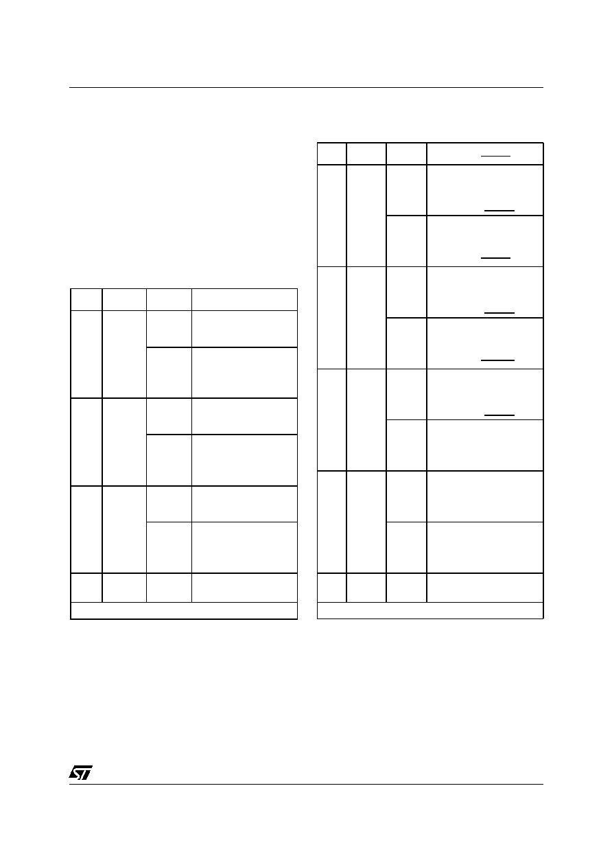
ST52T410/ST52T420/E420
45/84
PWM/Timers Alternate Functions
The pins of Port A and C can be configured to be I/
O of the three PWM/Timers available on the
ST52T410/ST52x420. The configuration of these
pins is performed by using the Configuration
Registers REG_CONF 12 and REG_CONF 16 if
the related pin has to be output. When the related
pin has to be used as an input peripheral the
configuration
is
performed
by
the
relative
peripheral configuration registers (See PWM/
Timer Session).
Warning:
in order to use PC1, PC2 and PC3
pins as standard I/O pins, the PWM/Timers
must be configured in Timer mode
Table 7.8 PWM/Timers REG_CONF 16
Bit
Name
Value
Description
0
PC1
1
Pin T0OUT/PC1 is
configured as Port C
Digital I/O
0
Pin T0OUT/PC1 is
configured as PWM/
Timer 0 output T0OUT
1
PC2
1
PinT1OUT/PC2 is
configured as Port C
Digital I/O
0
Pin T1OUT/PC2 is
configured as PWM/
Timer 1 output T1OUT
2
PC3
1
Pin T2OUT/PC3 is
configured as Port C
Digital I/O
0
Pin T2OUT/PC3 is
configured as PWM/
Timer 2 output T2OUT
3-7
NC
X
Not Used
Reset Configuration `00000000
Table 7.9 PWM/Timers REG_CONF 12
Bit
Name
Value
Description
0
PA1
1
Pin PA1/T0OUT is
configured as
PWM/Timer 0
complementary output
0
Pin PA1/T0OUT is
configured as
Port A Digital I/O
1
PA2
1
Pin PA2/T1OUT is
configured as
PWM/Timer 1
complementary output
0
Pin PA2/T1OUT is
configured as
Port A Digital I/O
2
PA3
1
Pin PA3/T2OUT is
configured as
PWM/Timer 2
complementary output
0
Pin PA3/T2OUT is
configured as
Port A Digital I/O
3
PASZ
1
PORT A bits = 8
0
PORT A bits = 7
4-7
NC
x
Not Used
Reset Configuration `0000'

ST52T410/ST52T420/E420
46/84
Figure 7.3 Configuration Register 12
Figure 7.4 Configuration Register 16
D7 D6 D5 D4 D3 D2 D1 D0
PA1T: Pin PA1/T0OUT setting
not used
REG_CONF 12
DIGITAL PORT
PA2T: Pin PA2/T1OUT setting
PA3T: Pin PA3/T2OUT setting
PA78: PORT A size

ST52T410/ST52T420/E420
47/84
8 A/D CONVERTER (ST52X420 ONLY)
8.1 Introduction
The A/D Converter of ST52x420 is an 8-bit analog
to digital converter with up to 8 analog inputs
offering 8 bit resolution with a total accuracy of 1
LSB and a typical conversion time of 8.2
µ
s with a
20 MHz clock. This period also includes the 5.1
µ
s
of the integral Sample and Hold circuitry, which
minimizes the need for external components and
allows quick sampling of the signal for a minimum
warping effect and Integral conversion error.
Conversion is performed in 82 A/D clock
pulses.
The A/D clock is derived from the clock master.
The maximum A/D clock frequency has to be 10
MHz. When the master clock is higher than 10
MHz it has to be divided by 2 using the SCK bit of
the A/D configuration register REG_CONF 3 (See
Table 8.1).
The A/D peripheral converts the input voltage with
a process of successive approximations using a
fixed clock frequency derived from the oscillator.
The conversion range is between the analog
V
SS
and V
DD
references.
The converter uses a fully differential analog input
configuration for the best noise immunity and
Figure 8.1 A/D Converter Structure
precision performance, along with one separate
supply (V
DDA
), allowing the best supply noise
rejection.
Up to 8 multiplexed Analog Inputs are available. A
group of signals can be converted sequentially by
simply programming the starting address of the
last analog channel to be converted.
Single
or
continuous
conversion
mode
are
available.
The result of the conversion is stored in an 8-bit
Input Register (from IR 1 to IR 8).
The
A/D
converter
is
controlled
via
the
Configuration Register REG_CONF 3.
A Power-Down programmable bit allows the A/D
converter to be set to a minimum consumption idle
status.
The
ST52x420
Interrupt
Unit
provides
one
maskable channel for the End of Conversion
(EOC).
8.2 Operational Description
The conversion is monotonic, meaning that the
result never decreases if the analog input doesn't
and never increases if the analog input doesn't.
If input voltage is greater than or equal to V
dda
(Voltage Reference high) then the result is equal to
FFh (full scale) without an overflow indication.
PB0/AIN0
PB1/AIN1
PB2/AIN2
PB3/AIN3
PB7/PA7/AIN7
PB6/AIN6
PB5/AIN5
PB4/AIN4
ANALOG
MUX
SUCCESSIVE APPROXMATION
A/D CONVERTER
A/D CHANNEL 7
A/D CHANNEL 6
A/D CHANNEL 5
A/D CHANNEL 4
A/D CHANNEL 3
A/D CHANNEL 2
A/D CHANNEL 1
A/D CHANNEL 0
INPUT REGISTER
1 ˜ 8
SAMPLE
HOLD
&
CH2
CH1
CH0
SCK
SEQ
POW
LP
STR
CONFIGURATION REGISTER 3
CONTROL
LOGIC
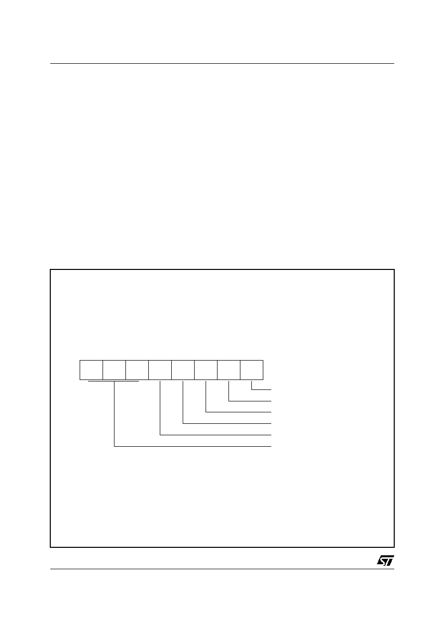
ST52T410/ST52T420/E420
48/84
If input voltage is less than V
SS
(voltage reference
low) then the result is equal to 00h.
The A/D converter is linear and the digital result of
the conversion is provided by the following
formula:
Where Reference Voltage is V
dda
- V
ss
.
The accuracy of the conversion is described in the
Electrical Characteristics Section.
The A/D converter is not affected by the WAIT
mode.
When the MCU enters HALT mode with A/D
converter enabled, the converter is disabled until
HALT mode is terminated and the start-up delay
has elapsed. A stabilization period is also required
before accurate conversions can be performed.
Figure 8.2 Conf. Register (REG_CONF 3)
8.2.1 Operating Modes.
Four main operating modes can be selected by
setting the values of the LP and SEQ bit in the A/D
configuration Register.
One Channel Single Mode
In this mode (SEQ = `0'', LP = `0') the A/D provides
an EOC signal after the end of channel i-th
conversion; then the A/D waits for a new start
event. Channel i-th is identified by the bit CH0,
CH1, CH2.
i.e CH(2:0) = `011' means conversion of channel 3
then stop.
Multiple Channels Single Mode
In this mode (SEQ = `1', LP = `0') the A/D provides
an EOC signal after the end of the channels
sequence conversion identified by the bit CH0,
CH1, CH2; then the A/D waits for a new start event.
i.e. CH(2:0) = `011' means conversion of channels
0,1,2 and 3 then stop.
Digitalr es ult
255inputVoltage
re fe re nce V oltage
------------------------------------------------
=
D 7
D0
CH2 CH1 CH0 SCK SEQ POW
LP STR
REG_CONF 3
START/STOP
CONVERSION MODE SEL.
ON/OFF A/D
CONVERSION MODE SEL.
CLOCK SELECTOR
CHANNELS SEL.
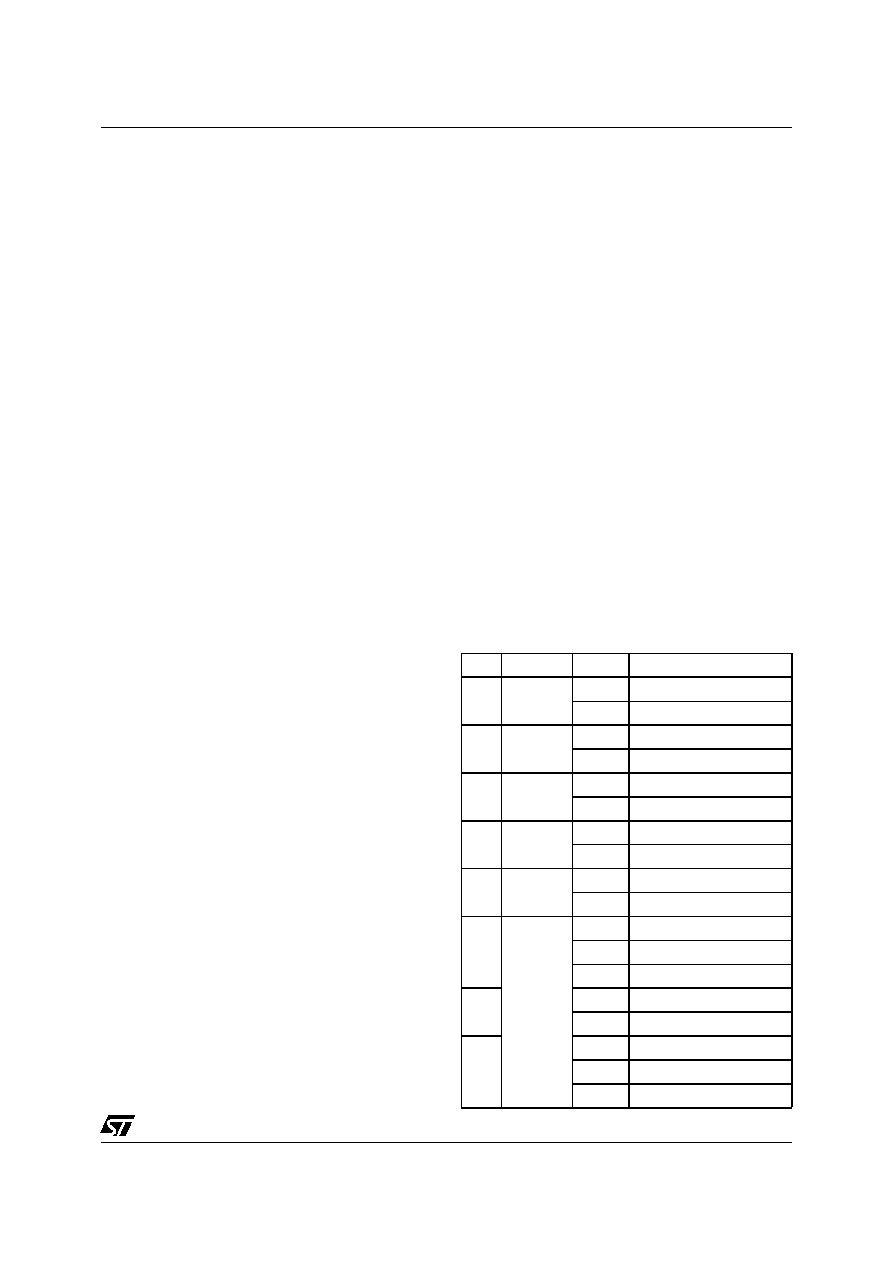
ST52T410/ST52T420/E420
49/84
One Channel Continuous Mode
In this mode (SEQ = `0'', LP = `1') a continuous
conversion flow is entered by a starting event on
the channel selected by the CH0, CH1, CH2 bits
For example: CH(2:0) = `011' means continuous
conversion of channel 3. At the end of each
conversion the relative IR is updated with the last
conversion result, while the former value is lost.
To stop the conversion STR has to be set to `0'.
Multiple Channels Continuous Mode
In this mode (SEQ = `1'', LP = `1') a continuous
conversion flow is entered by a starting event on
the channels selected by the CH0, CH1, CH2 bits.
i.e CH(2:0) = `011' means continuous conversion
of channel 0,1,2 and 3.
At the end of each conversion the relative IRs are
updated with the last conversion results, while the
former values are lost.
To stop the conversion STR has to be set to `0'.
8.2.2 Power Down Mode.
Before enabling any A/D operation mode, set the
POW bit of the A/D configuration register to `1' at
least 60
µ
s before the first conversion starts to
enable the biasing circuit inside the analog section
of the converter. Clearing the POW bit (POW = `0')
is useful when the A/D is not used, reducing the
total chip power consumption. This state is also the
reset configuration and it is forced by hardware
when the core is in HALT state (after a HALT
instruction execution).
8.3 A/D Registers Description
The result of the conversions of the 8 available
channels are loaded in the 8 Input Register from
decimal address 1 to decimal address 8. (IR (1:8)
see Table 2.2)). Every IR(1:8) is reloaded with a
new value at the end of the conversion of the
correspondent analog input.
By using the assembler instruction:
LDRI RAM_Reg. IR_i
the value stored in the i-th IR is transferred on the
RAM location RAM_Reg.
The A/D configuration register is the REG_CONF
3. Figure 7.2 illustrates the structure of this
register, which manages the A/D logic operation.
The A/D configuration register (REG_CONF 3) is
programmable as following:
b7-b5 = CH2, CH1, CH0: Last Conversion
Address. These 3 bits define the last analog input.
The first analog input is converted, then the
address
is
incremented
for
the
successive
conversion until the channel identified by CH0-
CH2 is converted. The (CH2, CH1, CH0) bits
define the group of channels to be scanned. When
setting CH2=0 CH1=0 CH0=0 only channel 0 is
converted.
b4 = SCK: Master clock divider. ST52x420 can
work with a clock frequency up to 20 MHz. The
SCK must be set to `1' when the ST52x420 clock is
higher then 10 MHz. It is useful to set SCK = `1'
even when the clock master is lower than 10 MHz
and a high accuracy is required.
b3 = SEQ: Multiple/Single channel. When SEQ is
set to `0' the channel identified by CH(2:0) is
converted. If SEQ is set to `1' the group of channels
identified by CH(2:0) are converted.
b2= POW: Power Up/ Power Down. A logical `1'
enables the A/D logic and analog circuitry.
Logical level `0' disables all power consuming
logic, allowing a low power idle status.
b1 = LP: Continuous/Single. When this bit is set to
`1'
(continuous
mode),
the
first
conversion
sequences are started by the STR bit then a
continuous conversion flow is processed.
When LP='0' (single mode) only one sequence of
conversions is started when STR is set.
b0 = STR: Start/Stop. A logical level `1' enables
starting a conversion sequence; a logical level `0'
stops the conversion. When the A/D is running in
the Single Modes (LP='0'), this bit is hardware
reset at the end of a conversion sequence.
Table 8.1 A/D Conf. Register (Reg_Conf 3)
Bit
Name
Value
Description
0
STR
0
Stop Conversion
1
Start Conversion
1
LP
0
Single Conversion
1
Continuous
2
POW
0
A/D OFF
1
A/D ON
3
SEQ
0
Single Channel Conv.
1
Multiple Channels Conv
4
SCK
0
Clock not Divided
1
Clock Divided
5
CH(2:0)
000
Channel 0
001
Channel 1
010
Channel 2
6
011
Channel 3
100
Channel 4
7
101
Channel 5
110
Channel 6
111
Channel 7
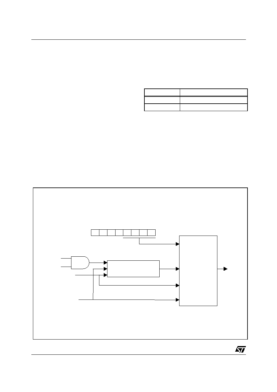
ST52T410/ST52T420/E420
50/84
9 WATCHDOG TIMER
9.1 Operational Description
The Watchdog Timer (WDT) is used to detect the
occurrence of a software fault, usually generated
by external interference or by unforeseen logical
conditions, which cause the application program to
abandon its normal sequence. The WDT circuit
generates
an
MCU
reset
on
expiry
of
a
programmed time period, unless the program
refreshes the WDT before the end of the
programmed time delay.
16 different delays can be selected by using the
WDT configuration register.
After the end of the delay programmed by the
configuration register if the WDT is activated (by
using the assembler instruction WDTSFR), it starts
a reset cycle pulling the reset pin low.
Once the WDT has been activated the application
program has to refresh this peripheral (by the
WDTSFR
instruction) at regular intervals during
normal operation in order to prevent an MCU reset.
In order to stop the WDT during user program
execution the instruction
WDTSLP
has to be used.
Figure 9.1 Watchdog Block Diagram
The working frequency of the WDT (PRES CLK in
the Figure 9.1) is equal to the clock master. The
clock master is divided by 500, obtaining the WDT
CLK signal, which is used to fix the timeout of the
WDT.
According to the WDT configuration register
values, a WDT delay may be defined between 0.1
ms and 937.5 mS when the clock master is 5 MHz.
By changing the clock master frequency the
timeout delay can be calculated according to the
configuration register values REG_CONF 2, as
described in the following section.
Warning: changing the REG_CONF2 value when
the WDT is active, a WDT reset is generated and
the CPU is restarted. To avoid this side effect, use
the
WDTSLP
instruction before changing the
REG_CONF2.
Table 9.1 Watchdog Timing range (CLK=5
MHz)
WDT timeout period (ms)
min
0.1
max
937.5
D0
D1
D2
D3
REG_CONF 2
RESET
WDTRFR
PRES CLK = CLK MASTER
WDTSLP
PRESCALER
WDT
RESET
GENERATOR
RESET
WTD CLK

ST52T410/ST52T420/E420
51/84
9.2 Register Description
The WDT timeout is defined by setting the value of
the REG_CONF 2. The first 4 bits of this register
are
used,
obtaining
16
different
delays
as
illustrated in Table 9.2. In Table 9.2 timeout is
expressed by using the number of WDT CLK. The
WDT CLK is derived from the clock master by a
division factor of 500. Timeout is obtained by
multiplying the WDT CLK pulse length for the
number of pulses defined by the configuration
register REG_CONF 2. Table 9.4 illustrates the
pulse lengths for typical values of the clock master.
Table 9.3 illustrates the timeout WDT values when
the Master Clock is 5 MHz.
Table 9.2 WDT REG_CONF 2
Bit
Name
Value
Timeout Values (WDT)
0
D(3:0)
0000
1
0001
625
0010
1250
0011
1875
1
0100
2500
0101
3125
0110
3750
0111
4375
2
1000
5000
1001
5625
1010
6250
1011
6875
3
1100
7500
1101
8125
1110
8750
1111
9375
4-7
NC
x
Not Used
Reset Configuration `0000'
Table 9.3 Timeout Values with CLK = 5 MHz
Bit
Name
Value
Timeout Values (ms)
0
D (3:0)
0000
0.1
0001
62.5
0010
125
0011
187.5
1
0100
250
0101
312.5
0110
375
0111
437.5
2
1000
500
1001
562.5
1010
625
1011
687.5
3
1100
750
1101
812.5
1110
875
1111
937.5
4-7
NC
x
Not Used
Reset Configuration `0000'
Table 9.4 Typical WDT CLK Pulse Length
MASTER CLK
(MHz)
WDT CLK
(KHz)
WDT CLK
PULSE
LENGTH (ms)
4
8
0.125
5
10
0.1
8
16
0.0625
10
20
0.05
20
40
0.025

ST52T410/ST52T420/E420
52/84
10 PWM/TIMER
ST52T410/ST52x420 offers three on-chip PWM/
Timer peripherals:TIMER0, TIMER1 and TIMER2.
The ST52T410/ST52x420 timers have the same
internal structure. The timer consists of an 8-bit
counter with a 16-bit programmable prescaler,
giving a maximum count of 2
24
(see Figure 10.1).
Figure 10.1 Timer Peripheral Block Diagram
Next, the generic timer is called Timer x, where x
can be 0, 1 or 2.
Each timer has two different working modes, which
can be selected by setting the correspondent
TxMODE bits of REG_CONF5, REG_CONF8 and
REG_CONF10 registers: Timer Mode and PWM
(Pulse Width Modulation) Mode.
All Timers have Autoreload Functions in PWM
Mode.
Each
timer
output
is
available,
with
its
complementary signal on external pins by setting
PAx
and
PCx
bits
of
REG_CONF12
and
REG_CONF16 (see Table 10.8 and Table 10.9).
Note: In order to enable timer output (TxOUT or
TxOUT) the related pin must be configured in
Output Mode by setting REG_CONF4 and
REG_CONF15 registers (see Table 7.4 and
Table 7.6)
In particular, TIMER0 can also use external
START/STOP signals (Input capture and Output
compare), external RESET signal and external
CLOCK: PA4/T0STRT, PA0/T0RES and PA5/
T0CLK pins.
Note: In order to use T0RST, T0STR, T0CLK
external signals the related pins must be
configured
in
Input
Mode
by
setting
REG_CONF4 and REG_CONF7 registers (see
Table 7.4 and Table 10.3)
For each timer, the content of the 8-bit counter is
incremented on the Rising Edge of the 16-bit
prescaler output (PRESCOUT) and it can be read
at any instant of the counting phase, saved in a
location of RAM memory. The PWM/Timer x
Counter value can be read from the Input Register
PWM_x_COUNT (Input Registers 12, 14 or 16.
See Table 2.2).
The PWM/Timer x Status can be read from the
Input Register PWM_x_STATUS (Input Registers
13, 15 or 17. See Table 2.2 and Table 10.10).
10.1 Timer Mode
Timer Mode is selected by fixing the TxMODE bit
of
REG_CONF5,
REG_CONF8
and
REG_CONF10 equal to 0 (see Table 10.1, Table
10.4 and Table 10.6).
Each TIMERx requires three signals: Timer Clock
(TMRCLKx), Timer Reset (TxRES) and Timer Start
(TxSTRT) (see Figure 10.1). Each of these signals
can be generated internally, or, only for Timer 0,
externally by setting T0RST, T0STR, T0CLK bits of
REG_CONF7 register.
TMRCLKx is the Prescaler x output, which
increments the Counter x value on the rising edge.
TMRCLKx is obtained from the internal clock
signal (CLKM) or, only for TIMER0, from the
external signal provided on the PA5/T0CLK pin.
BIT0
BIT1
BIT2
BIT3
BIT4
BIT5
BIT14
BIT15
BIT3
BIT0
BIT1
BIT2
BIT6
BIT4
BIT5
BIT7
17- 1MULTIPLEXER
16-BITPRESCALER
8-BITCOUNTER
PRESCx
CLKM
TMRCLK
TxRES
TxSTRT

ST52T410/ST52T420/E420
53/84
Figure 10.2 Timer 0 External START/STOP Mode
NOTE: The external clock signal applied on the
T0CLK pin must have a frequency at least two
times smaller than the internal master clock.
The prescaler output can be selected by setting the
PRESCx bit of REG_CONF6, REG_CONF9 and
REG_CONF11 registers (see Table 10.2, Table
10.5 and Table 10.7).
REMARK: The first period of the TxOUT signal
is one clock cycle shorter.
TxRES resets the content of the 8-bit counter x to
zero. It is generated by the TIRSTx and TxMSK
bits of REG_CONF5, REG_CONF7, REG_CONF8
and REG_CONF10 registers (see Table 10.1,
Table 10.3, Table 10.4 and Table 10.6).
TxSTRT signal starts/stops Timer x counting only
if the peripherals are configured in Timer mode.
This signal is forced by setting the correspondent
TISTRx bit of REG_CONF5, REG_CONF8 and
REG_CONF10 registers (see Table 10.1, Table
10.4 and Table 10.6).
TxMSK bits mask the reset of each timer and can
be utilized to synchronize a simultaneous start of
the timers by means (for example), of the following
procedure, which starts three timers:
1) TIRST0 = TIRST1 = TIRST2 = 0,
2) TISTR0 = TISTR1 = TISTR2 = 0,
3) T0MSK = T1MSK = T2MSK = 1,
4) TIRST0 = TIRST1 = TIRST2 = 1,
5) TISTR0 = TISTR1 = TISTR2 = 1,
6) T0MSK = T1MSK = T2MSK = 0,
When TxMSK is 1 the TIMER x is reset.
REMARK: to use the simultaneus start, the
prescalers of the Timers must have the same
value. Simultaneus start cannot be used in
Timer mode
Figure 10.3 TIMEROUT Signal Type
TIMER 0 START/STOP can be provided externally
on the T0STRT pin. In this case, the T0STRT
signal allows the user to work in two different
modes by setting the TESTR configuration bit of
REG_CONF5 register (see Figure 10.2) (Input
capture):
Level
Edge
start
stop
start
start
stop
start
0
1
1
0
4
4
3
2
Reset
Clock
Counted
Value
Timer Output
Type 1
Type 2
Prescout*Counter
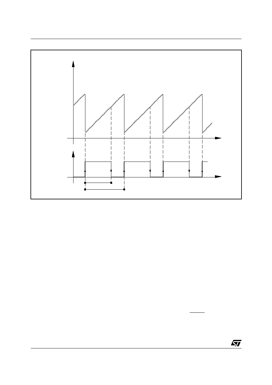
ST52T410/ST52T420/E420
54/84
Figure 10.4 PWM Mode with Auto Reload
LEVEL (Time Counter): If the T0STRT signal is
high the Timer starts counting. When T0STRT is
low the counting ceases and the current value is
stored in the PWM_0_COUNT Input Register.
EDGE(Period Counter): After reset, on the first
T0STRT rising edge, TIMER 0 starts counting and
at the next rising edge it stops. In this manner, the
period of an external signal may be measured.
Timer x output signal, TIMERxOUT is a signal with
a frequency equal to the 16 bit-Prescaler x output
signal, TMRCLKx, divided by the Output Register
PWM_x_COUNT value (8 bit) (Output Registers 3,
5 or 7. See Table 2.4), which is the value to count.
There can be two types of TIMERxOUT waveform:
type 1: TIMERxOUT waveform equal to a square
wave with a 50% duty-cycle.
type 2: TIMERxOUT waveform equal to a pulse
signal with the pulse duration equal to the
Prescaler x output signal.
For each Timer x, the TIMERxOUT waveform type
can be selected by setting the correspondent
TMRWx bit of REG_CONF6, REG_CONF9 and
REG_CONF11 registers (see Table 10.2, Table
10.5 and Table 10.7)
WARNING:
in
Timer
Mode
the
PWM_x_RELOAD output register (see below)
must be set to 0.
10.2 PWM Mode
For each timer, PWM working mode is obtained by
setting
the
correspondent
TxMODE
bits
of
REG_CONF5, REG_CONF8 and REG_CONF10
registers to 1 (see Table 10.1, Table 10.4 and
Table 10.6).
REMARK: The first period of the TxOUT signal
is
shorter than the other periods for a time
interval which is [0.5*TMRCLK-CLKM].
TIMERxOUT, in PWM Mode consists of a signal
with a fixed period, whose duty cycle can be
modified by the user.
The TIMERxOUT signal can be available on the
TxOUT pin and the TIMERxOUT inverted signal
can be available on the TxOUT pin by setting the
PxSL bits of REG_CONF12 and REG_CONF16
(see Table 10.8 and Table 10.9)
t
t
255
compare
value
reload
register
0
PWM
Output
Ton
T

ST52T410/ST52T420/E420
55/84
The PWM TIMERxOUT period can be determined
by setting the 16-bit prescaler x output and an
initial autoreload 8-bit counter value stored in the
Output Register PWM_x_RELOAD, as illustrated
in Figure 10.4.
NOTE: the Start/Stop and Set/Reset signals
should be moved together in PWM mode. If the
Start/Stop bit is reset during the PWM mode
working, the TxOUT signal keeps its status
until the next start.
The Output Register PWM_x_RELOAD value is
automatically reloaded when Counter x restarts
counting.
The 16-bit Prescaler x divides the master clock,
CLKM, or, only for TIMER0, the external T0CLK
signal, by the 16-bit Prescaler x.
NOTE: The external clock signal, applied on
T0CLK pin must have a frequency at least two
times smaller than the internal master clock.
The Prescaler x output can be selected by setting
PRESCx bit of REG_CONF6, REG_CONF9 and
REG_CONF11 registers (see Table 10.2, Table
10.5 and Table 10.7).
When Counter x reaches the Peripheral Register
PWM_x_COUNT
value
(Compare
Value),
TIMERxOUT signal changes from high to low level,
up to the next counter start.
The period of the PWM signal is obtained by using
the following equation:
T = (255 - PWM _x_RELOAD)x TMR CLKx
where TMRCLKx is the output of the 16-bit
prescaler x.
The duty cycle of the PWM signal is controlled by
the Output Register PWM_x_COUNT:
Ton =(PWM_x_COUNT- PWM_x_RELOAD)*
TMRCLKx
If the Output Register PWM_x_COUNT value is
255 the TIMERxOUT signal is always at a high
level.
If the Output Register PWM_x_COUNT is 0, or
less
than
the
PWM_x_RELOAD
value,
TIMERxOUT signal is always at a low level.
NOTE. If PWM_x_RELOAD value increases the
duty cycle resolution decreases. PWM cannot
work with a PWM_x_RELOAD value equal to
255.
By using a 20 MHz clock master a PWM frequency
in the range 1.2 Hz to 78.43 Khz can be obtained.
WARNING: loading new values of the counter
or of the reload in the Output Registers, the
PWM/Timer registers are immediately set on-
fly. This can cause some side effects during
the current counting cycle. The next cycles
work normally. This occurs both in Timer and
in PWM mode.
When the Timers are in Reset, or when the
device is reset, TxOut pins go in threestate. If
these outputs are used to drive external
devices it is recommended to put a pull-up or a
pull-down resistor.
10.3 Timer Interrupt
TIMERx can be programmed to generate an
Interrupt request at the end of the count or when
there is an external TSTART signal. The Timer can
generate programmable Interrupts into 4 different
modes:
Interrupt mode 1: Interrupt on counter Stop.
Interrupt mode 2: Interrupt on Rising Edge of
TIMEROUT.
Interrupt mode 3: Interrupt on Falling Edge of
TIMEROUT.
Interrupt mode 4: Interrupt on both edges of
TIMEROUT.
Interrupt mode can be selected by means of
INTSLx and INTEx bits of the REG_CONF5,
REG_CONF8 and REG_CONF10 registers (see
Table 10.1, Table 10.4 and Table 10.6).
NOTE: the interrupt on TIMEROUT rising edge
is also generated after the Start.
WARNING: the first interrupt after starting
PWM is not generated if the counter value is 0,
255, or lower than the reload value. If the PWM/
Timer is configured with the Interrupt on Stop
and the Start/Stop is configured as external, a
low signal in the STRT pin determines a PWM/
Timer interrupt even if the peripheral is off. If
the interrupt is configured on falling edge, a
reset signal generates an interrupt request.

ST52T410/ST52T420/E420
56/84
Figure 10.5 Configuration Register 5
Table 10.1 Configuration Register 5 Description
Bit
Name
Value
Description
0
TIRST0
0
PWM/TIMER 0 Internal RESET
1
PWM/TIMER 0 Internal SET
1
TERST
0
External RESET on Level
1
External RESET on Edge
2
TISTR0
0
PWM/TIMER 0 Internal STOP
1
PWM/TIMER 0 Internal START
3
TESTR
0
External START on Level
1
External START on Edge
4
INTE0
00
TIMER0 Interrupt on TIMER Interrupt on
TIMEROUT Falling Edge
01
TIMER0 Interrupt on
TIMER0OUT Rising Edge
5
10
TIMER0 Interrupt on Both Edges of TIMER0OUT
11
- not used
6
INTSL0
0
TIMER0 Interrupt on
Counter Stop
1
TIMER0 Interrupt on
TIMER0OUT
7
T0MODE
0
TIMER MODE
1
PWM MODE
D7 D6 D5 D4 D3 D2 D1 D0
TIRST0: Timer 0 Internal RESET
TERST: Timer 0 External RESET on Edge/Level
TISTR0: Timer 0 Internal START
TESTR: Timer 0 External START on Edge/Level
INTE0: Timer 0 Interrupt on TIMER0OUT Rising/Falling Edge
INTSL0: Timer 0 Interrupt Source selection
T0MODE: Timer 0 working mode
REG_CONF 5
TIMER 0
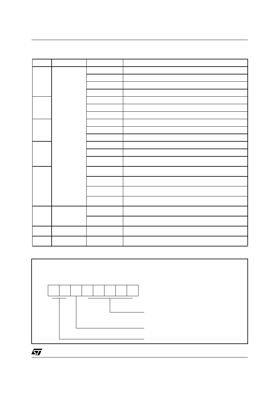
ST52T410/ST52T420/E420
57/84
Figure 10.6 Configuration Register 6
Table 10.2 Configuration Register 6 Description
Bit
Name
Value
Description
0
PRESC0
00000
TIMER0 Clock = CLKM / 1
00001
TIMER0 Clock = CLKM / 2
00010
TIMER0 Clock = CLKM / 4
00011
TIMER0 Clock = CLKM / 8
1
00100
TIMER0 Clock = CLKM / 16
00101
TIMER0 Clock = CLKM / 32
00110
TIMER0 Clock = CLKM / 64
2
00111
TIMER0 Clock = CLKM / 128
01000
TIMER0 Clock = CLKM / 256
01001
TIMER0 Clock = CLKM / 512
3
01010
TIMER0 Clock = CLKM/1024
01011
TIMER0 Clock = CLKM/2048
01100
TIMER0 Clock = CLKM/4096
4
01101
TIMER0 Clock = CLKM/8192
01110
TIMER0 Clock=CLKM/16384
01111
TIMER0 Clock=CLKM/32768
10000
TIMER0 Clock=CLKM /65536
5
TMRW0
0
TIMER0OUT Waveform equal to pulse wave
1
TIMER0OUT Waveform equal to square wave
6
-
-
- not used
7
-
-
- not used
D7 D6 D5 D4 D3 D2 D1 D0
PRESC0: Timer 0 Prescaler
TMRW 0: TIMER0OUT waveform
not used
REG_CONF 6
TIMER 0
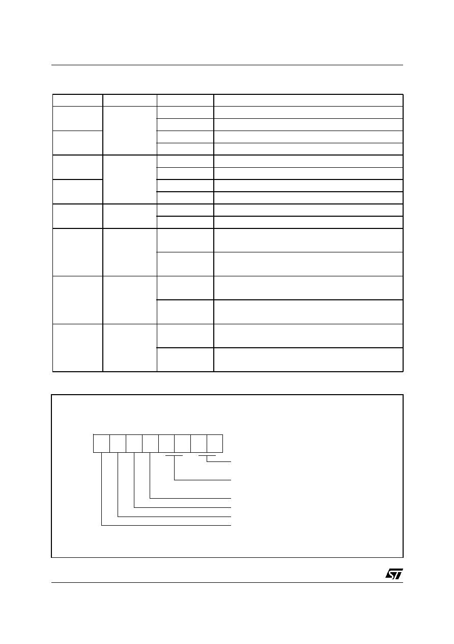
ST52T410/ST52T420/E420
58/84
Figure 10.7 Configuration Register 7
Table 10.3 Configuration Register 7 Description
Bit
Name
Value
Description
0
T0RST
00
TIMER0 RESET
01
TIMER0 RESET External
1
10
TIMER0 RESET External or Internal
11
- not used
2
T0STR
00
TIMER0 START Internal
01
TIMER0 START External
3
10
TIMER0 START External or Internal
11
- not used
4
T0CLK
0
TIMER0 Clock Internal
1
TIMER0 Clock External
5
T0MSK
0
TIMER 0 reset synchronization mask.
TIMER 0 RESET enabled
1
TIMER0 reset synchronization mask.
TIMER0 RESET masked
6
T2MSK
0
TIMER2 reset synchronization mask.
TIMER2 RESET enabled
1
TIMER2 reset synchronization mask.
TIMER2 RESET masked
7
T1MSK
0
TIMER1 reset synchronization mask.
TIMER1 RESET enabled
1
TIMER1 reset synchronization mask.
TIMER1 RESET masked
D7 D6 D5 D 4 D3 D2 D1 D0
T0RST: Tim er 0 RESET Mode
T0STR : Tim er 0 START Mode
T0CLK: Tim er 0 Clock Source
T0MSK: Tim er 0 RESE T Mask
T2MSK: Tim er 2 RESE T Mask
T1MSK: Tim er 1 RESE T Mask
REG_CONF 7
TIMER 0, TIMER 1, TIMER2

ST52T410/ST52T420/E420
59/84
Figure 10.8 Configuration Register 8
Table 10.4 Config. Register 8 Description
Bit
Name
Value
Description
0
TIRST1
0
PWM\TIMER 1 Internal RESET
1
PWM\TIMER 1 Internal SET
1
-
-
- not used
2
TISTR1
0
PWM/TIMER 1 Internal STOP
1
PWM/TIMER 1 Internal START
3
-
-
- not used
4
INTE1
00
TIMER1 Interrupt on TIMER1OUT Falling Edge
01
TIMER1 Interrupt on TIMER1OUT Rising Edge
5
10
TIMER1 Interrupt on Both Edges of TIMER1OUT
11
- not used
6
INTSL1
0
TIMER1 Interrupt on Counter Stop
1
TIMER1 Interrupt on TIMER1OUT
7
T1MODE
0
TIMER MODE
1
PWM MODE
D7 D6 D5 D4 D3 D2 D1 D0
TIRST1: Timer 1 RESET
- not used
TISTR1: Timer 1 START
- not used
INTE1: Timer 1 Interrupt on TIMER1OUT Rising/Falling Edge
INTSL1: Timer 1 Interrupt Source selection
T1MODE: Timer 1 working mode
REG_CONF 8
TIMER 1

ST52T410/ST52T420/E420
60/84
Figure 10.9 Configuration Register 9
Table 10.5 Config. Register 9 Description
Bit
Name
Value
Description
0
PRESC1
00000
TIMER1 Clock = CLKM / 1
00001
TIMER1 Clock = CLKM / 2
00010
TIMER1 Clock = CLKM / 4
00011
TIMER1 Clock = CLKM / 8
1
00100
TIMER1 Clock = CLKM / 16
00101
TIMER1 Clock = CLKM / 32
00110
TIMER1 Clock = CLKM / 64
2
00111
TIMER1 Clock = CLKM / 128
01000
TIMER1 Clock = CLKM / 256
01001
TIMER1 Clock = CLKM / 512
3
01010
TIMER1 Clock =CLKM / 1024
01011
TIMER1 Clock =CLKM / 2048
01100
TIMER1 Clock =CLKM / 4096
4
01101
TIMER1 Clock =CLKM / 8192
01110
TIMER1 Clock =CLKM/16384
01111
TIMER1 Clock=CLKM /32768
10000
TIMER1 Clock=CLKM /65536
5
TMRW1
0
TIMER1OUT Waveform equal to pulse wave
1
TIMER1OUT Waveform equal to square wave
6
-
-
- not used
7
-
-
- not used
D7 D6 D5 D4 D3 D2 D1 D0
PRESC1: Timer 1 Prescaler
TMRW1: TIMER1OUT waveform
not used
REG_CONF 9
TIMER 1

ST52T410/ST52T420/E420
61/84
Figure 10.10 Configuration Register 10
Table 10.6 Config. Register 10 Description
Bit
Name
Value
Description
0
TIRST2
0
PWM/TIMER 2 Internal RESET
1
PWM/TIMER 2 Internal SET
1
-
-
- not used
2
TISTR2
0
PWM/TIMER 2 Internal STOP
1
PWM/TIMER 2 Internal START
3
-
-
- not used
4
INTE2
00
TIMER2 Interrupt on TIMER2OUT Falling Edge
01
TIMER2 Interrupt on TIMER2OUT Rising Edge
5
10
TIMER2 Interrupt on Both Edges of TIMER2OUT
11
- not used
6
INTSL2
0
TIMER2 Interrupt on Counter Stop
1
TIMER2 Interrupt on TIMER2OUT
7
T2MODE
0
TIMER MODE
1
PWM MODE
D7 D6 D5 D4 D3 D2 D1 D0
TIRST2: Timer 2 RESET
- not used
TISTR2: Timer 2 START
- not used
INTE2: Timer 2 Interrupt on TIMER2OUT Rising/Falling Edge
INTSL2: Timer 2 Interrupt Source selection
T2MODE: Timer 2 working mode
REG_CONF 10
TIMER 2

ST52T410/ST52T420/E420
62/84
Figure 10.11 Configuration register 11
Table 10.7 Config. Register 11 Description
Bit
Name
Value
Description
0
PRESC2
00000
TIMER2 Clock = CLKM / 1
00001
TIMER2 Clock = CLKM / 2
00010
TIMER2 Clock = CLKM / 4
1
00011
TIMER2 Clock = CLKM / 8
00100
TIMER2 Clock = CLKM / 16
00101
TIMER2 Clock = CLKM / 32
00110
TIMER2 Clock = CLKM / 64
2
00111
TIMER2 Clock = CLKM / 128
01000
TIMER2 Clock = CLKM / 256
01001
TIMER2 Clock = CLKM / 512
3
01010
TIMER2 Clock = CLKM /1024
01011
TIMER2 Clock = CLKM/ 2048
01100
TIMER2 Clock = CLKM/ 4096
4
01101
TIMER2 Clock = CLKM/ 8192
01110
TIMER2 Clock= CLKM/16384
01111
TIMER2 Clock =CLKM/32768
10000
TIMER2 Clock =CLKM/65536
5
TMRW2
0
TIMER2OUT Waveform equal to pulse wave
1
TIMER2OUT Waveform equal to square wave
6
-
-
- not used
7
-
-
- not used
D7 D6 D5 D4 D3 D2 D1 D0
PRESC2: Timer 2 Prescaler
TMRW2: TIMER2OUT waveform
not used
REG_CONF 11
TIMER 2

ST52T410/ST52T420/E420
63/84
Figure 10.12 Configuration Register 12
Table 10.8 Config. Register 12 Description
Bit
Name
Value
Description
0
PA1
0
Pin PA1/T0OUT equal to PORT A Digital I/O
1
Pin PA1/ T0OUT equal to T0OUT
1
PA2
0
Pin PA2/ T1OUT equal to PORT A Digital I/O
1
Pin PA2/ T1OUT equal to T1OUT
2
PA3
0
Pin PA3/ T2OUT equal to PORT A Digital I/O
1
Pin PA3/ T2OUT equal to T2OUT
3
PASZ
0
PORT A bits = 7
1
PORT A bits = 8
4
-
-
- not used
5
-
-
- not used
6
-
-
- not used
7
-
-
- not used
D7 D6 D5 D4 D3 D2 D1 D0
PA1: Pin PA1/T0OUT setting
not used
REG_CONF 12
DIGITAL PORT
PA2: Pin PA2/T1OUT setting
PA3: Pin PA3/T2OUT setting
PASZ: PORT A size
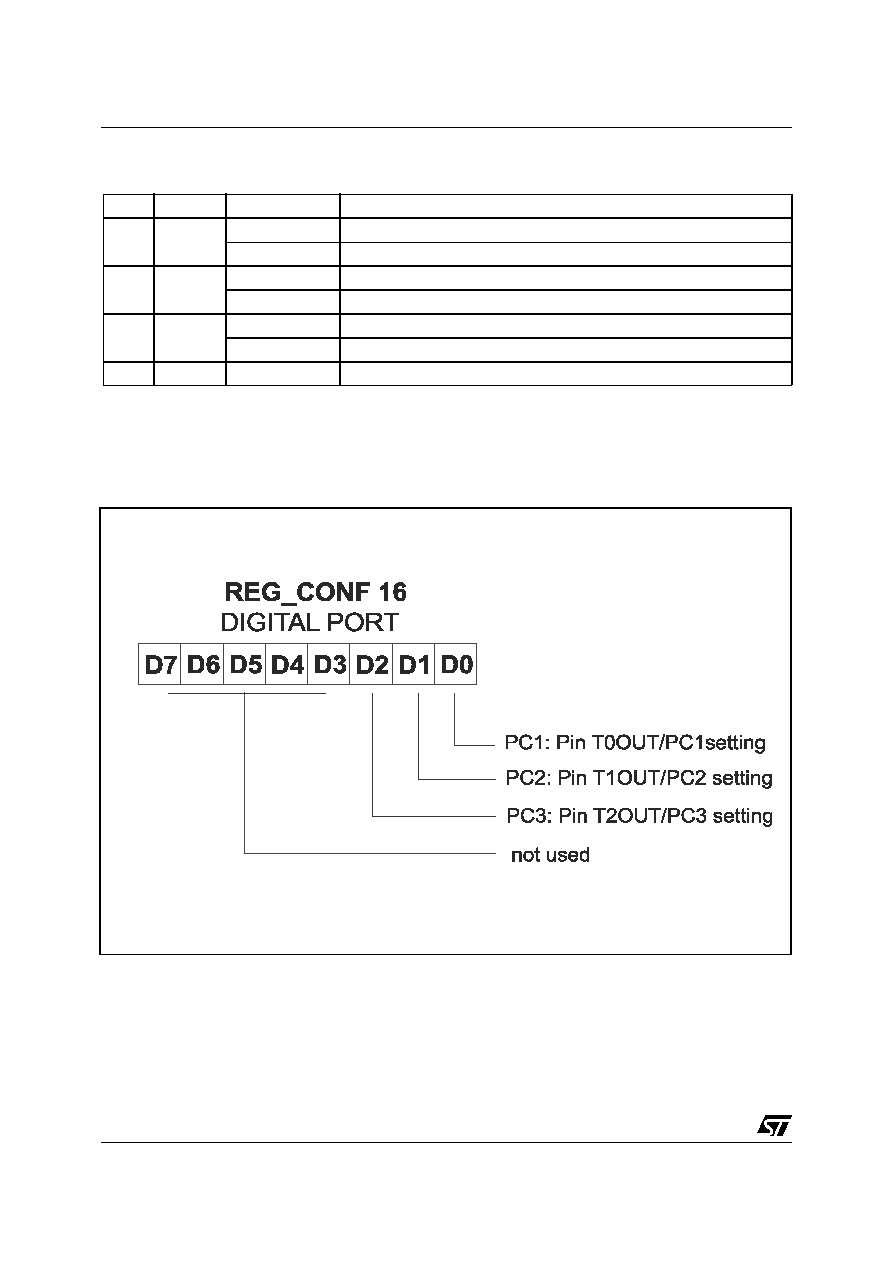
ST52T410/ST52T420/E420
64/84
Figure 10.13 Configuration Register 16
Table 10.9 Config. Register 16 Description
Bit
Name
Value
Description
0
PC1
1
Pin T0OUT/PC1 equal to PORT C Digital I/O
0
Pin T0OUT/PC1 equal to T0OUT
1
PC2
1
Pin T1OUT/PC2 equal to PORT C Digital I/O
0
Pin T1OUT/PC2 equal to T1OUT
2
PC3
1
Pin T2OUT/PC3 equal to PORT C Digital I/O
0
Pin T2OUT/PC3 equal to T2OUT
3-7
-
-
- not used
ST52T410/ST52T420/E420
65/84
Table 10.10 Input Registers 13.
PWM_0_STATUS
Bit
Name
Value
Description
0
STR0
0
TIMER 0 is STOP
1
TIMER 0 START
1
RST0
0
TIMER 0 is RESET
1
TIMER 0 is NOT
RESET
2
-
-
- not used
3
-
-
- not used
4
-
-
- not used
5
-
-
- not used
6
-
-
- not used
7
-
-
- not used
Table 10.11 Input Registers 15.
PWM_1_STATUS
Bit
Name
Value
Description
0
STR1S
0
TIMER 1 is STOP
1
TIMER 1 is START
1
RST1S
0
TIMER 1 is RESET
1
TIMER 1 is NOT
2
-
-
- not used
3
-
-
- not used
4
-
-
- not used
5
-
-
- not used
6
-
-
- not used
7
-
-
- not used
Table 10.12 Input Registers 17.
PWM_2_STATUS
Bit
Name
Value
Description
0
STR2
0
TIMER 2 is STOP
1
TIMER 2 is START
1
RST2
0
TIMER 2 is RESET
1
TIMER 2 is NOT
RESET
2
-
-
- not used
3
-
-
- not used
4
-
-
- not used
5
-
-
- not used
6
-
-
- not used
7
-
-
- not used

ST52T410/ST52T420/E420
66/84
11 ELECTRICAL CHARACTERISTICS
11.1 Parameter Conditions
Unless otherwise specified, all voltages are
referred to V
ss.
11.1.1 Minimum and Maximum values.
Unless otherwise specified, the minimum and
maximum values are guaranteed in the worst
conditions of environment temperature, supply
voltage and frequencies production testing on
100% of the devices with an environmental
temperature at T
A
=25
∞
C and T
A
=T
A
max (given by
the selected temperature range).
Data is based on characterization results, design
simulation and/or technology characteristics are
indicated in the table footnotes and are not tested
in production. The minimum and maximum values
are based on characterization and refer to sample
tests, representing the mean value plus or minus
three times the standard deviation (mean
±
3
).
11.1.2 Typical values.
Unless otherwise specified, typical data is based
on T
A
=25
∞
C, V
DD
=5V (for the 4.5
V
DD
5.5V
voltage range). They are provided only as design
guidelines and are not tested.
11.1.3 Typical curves.
Unless otherwise specified, all typical curves are
provided only as design guidelines and are not
tested.
Figure 11.1 Pin loading conditions
11.1.4 Loading capacitor. The loading condition
used for pin parameter measurement is illustrated
in Figure 11.1.
11.1.5 Pin input voltage.
Input voltage measurement on a pin of the device
is described in Figure 11.2
Figure 11.2 Pin input Voltage
11.2 Absolute Maximum Ratings
Stresses above those listed as "absolute maximum
ratings" may cause permanent damage to the
device. This is a stress rating only.
Functional operation of the device under these
conditions is not implied. Exposure to maximum
rating conditions for extended periods may affect
device reliability.
ST52 PIN
C
L
ST52 PIN
V
IN

ST52T410/ST52T420/E420
67/84
Table 11.1 Voltage Characteristics
Symbol
Ratings
Maximum Value
Unit
V
DD
-V
SS
Supply voltage
6.5
V
V
DDA
-V
SSA
Analog reference voltage(V
DD
V
DDA
)
6.5
|
V
DDA
|
and
|
V
SSA
|
Variation between different digital power pins
50
mV
|
V
SSA
-V
SSX
|
Variation between digital and analog ground pins
50
V
IN
Input voltage on Vpp
V
SS
-0.3 to 13
V
Input voltage on any other pin
1) & 2)
V
SS
-0.3 to V
DD
+0.3
V
DESD
Electro-static discharge voltage
2000
Table 11.2 Current Characteristics
Symbol
Ratings
Maximum Value
Unit
I
VDD
Total current in V
DD
power lines (source)
3)
100
mA
I
VSS
Total current in V
SS
ground lines (sink)
3)
100
I
IO
Standard Output Source Sink current
±
16
I
INJ(PIN)
Injected current on V
PP
pin
±
5
Injected current on RESET pin
±
5
Injected current on OSCin and OSCout pins
±
5
Injected current on any other pin
4)
±
5
I
INJ(PIN)
Total Injected current (sum of all I/O and control
pins)
4)
±
20
Table 11.3 Thermal Characteristics
Symbol
Ratings
Maximum Value
Unit
T
A
Operating temperature
-25 to +85
∞
C
T
STG
Storage temperature range
-65 to +150
∞
C
T
J
Maximum junction temperature
150
∞
C
Notes:
1. Connecting RESET and I/O Pins directly to V
DD
or V
SS
could damage the device if the unintentional internal reset is generated
or an unexpected change of I/O configuration occurs (for example, due to the corrupted program counter). In order to guarantee
safe operation, this connection has to be performed via a pull-up or pull-down resistor (typical: 4.7k
for RESET, 10K
for I/Os).
Unused I/O pins must be tied in the same manner to V
DD
or V
SS
according to their reset configuration.
2. When the current limitation is not possible, the VIN absolute maximum rating must be respected, otherwise refer to I
INJ(PIN)
specification. A positive injection is induced by V
IN
>V
DD
while a negative injection is induced by V
IN
<V
SS
to I
INJ(PIN)
specification.
A positive injection is VIN>VDD while a negative injection is induced by V
IN
<V
SS
.
3. All power (V
DD
) and ground (V
SS
) lines must always be connected to the external supply.
4. When several inputs are submitted to a current injection, the maximum
I
INJ(PIN)
is the absolute sum of the positive and negative
injected currents (instantaneous values).

ST52T410/ST52T420/E420
68/84
11.3 Recommended Operating Condition
Operating condition: V
DD
=5V
±
10%; T
A
= -25/85
∞
C (unless otherwise specified).
Notes:
1. The maximum difference between V
SS
and V
SSA,
and between V
DD
and V
DDA,
must be less than 0.6 V
in module. The minimum value of V
DDA
is 3 V.
2. V
DD
depend on
f
OSC ,
see Figure 11.3
3. The
f
OSC
min allowed to use the A/D Converter is 2 MHz
4. Lower V
DD
decreasing f
osc
(see Figure 11.3). Data illustrated in the figure are characterized but not test-
ed.
Figure 11.3 fosc Maximum Operating Frequency versus VDD supply
Table 11.4 Recommended Operating Conditions
Symbol
Parameter
Test Condition
Min.
Typ.
Max
Unit
V
DD
Operating Supply
1)2)
Refer to Figure 11.3
4.75
5.0
5.25
V
V
PP
Programming Voltage
11.4
12
12.6
V
O
Output Voltage
V
SS
V
DD
V
DDA,
V
SSA
Analog Supply Voltage
1)
V
SS
V
SSA
V
DDA
V
DD
V
SS
V
DD
f
OSC
1)2)
Oscillator Frequency
1
20
MHz
0
0.5
1
1.5
2
2.5
3
3.5
4
4.5
5
5.5
0
2
4
6
8
10
12
14
16
18
20
Functionality not guarateed in this area
Functionality not guarateed in this area
Functionality guarateed in this area
Vdd (V)
f
osc
.
ma
x
(
MH
z)

ST52T410/ST52T420/E420
69/84
11.4 Supply Current Characteristics
Supply current is mainly a function of the operating
voltage and frequency. Other factors such as I/O
pin loading and switching rate, oscillator type,
internal code execution pattern and temperature,
also have an impact on the current consumption.
The test condition in RUN mode for all the IDD
measurements are:
OSCin = external square wave, from rail to rail;
OSCout = floating;
All I/O pins tristated pulled to VDD
T
A
=25
∞
C
Figure 11.4 Typical IDD in RUN vs fosc
Figure 11.5 Typical IDD in WAIT vs fosc
Table 11.5 Supply Current in RUN and WAIT Mode
Symbol
Parameter
Conditions
Typ
Max
3)
Unit
I
DD
Supply current in RUN mode
1)
V
DD
=5V
±
5%
T
A
=25
∞
C
f
osc
=2 Mhz
4.34
4.34
mA
f
osc
=4 Mhz
7.66
7.72
f
osc
=5 Mhz
8.75
8.81
f
osc
=8 Mhz
12.67
12.89
f
osc
=10
15.04
15.13
f
osc
=20
27.3
27.48
Supply current in WAIT mode
2)
f
osc
=2 MHz
1.14
1.16
f
osc
=4 MHz
3.38
3.39
f
osc
=5 MHz
3.63
3.71
f
osc
=8 Mhz
5.63
5.68
f
osc
=10
6.29
6.31
f
osc
=20
13.22
13.3
0
5
10
15
20
25
30
35
2
2.5
3
3.5
4
4.5
5
5.5
6
VDD[V]
IDD[
m
A
]
2MHz
4MHz
5MHz
8MHz
10MHz
20MHz
0
2
4
6
8
10
12
14
2
2.5
3
3.5
4
4.5
5
5.5
6
VDD[V]
I
D
D[
m
A
]
2MHz
4MHz
5MHz
8MHz
10MHz
20MHz
Notes:
1. CPU running with memory access, all I/O pins in input mode with a static value at V
DD
or V
SS
(no load),
all peripherals switched off; clock input (OSCin driven by external square wave).
2. CPU in WAIT mode with all I/O pins in input mode with a static value at V
DD
or V
SS
(no load), all
peripherals switched off; clock input (OSCin driven by external square wave).
3. Data based on characterization results, tested in production at V
DDmax
and f
oscmax
.

ST52T410/ST52T420/E420
70/84
Notes:
1. Typical data is based on TA = 25
∞
C
2. All I/O pins in input mode with a static value at V
DD
or V
SS
(no load)
Notes:
3. Typical data is based on T
A
=25
∞
C, V
DDA
=5 V.
4. Data is based on characterization results and isn't tested in production.
Table 11.6 Supply Current in HALT Mode
Symbol
Parameter
Conditions
Typ
1)
Max
Unit
I
DDA
Supply current in HALT mode
2)
3.0 V
VDD
5.5 V
1
10
µ
A
Table 11.7 On-Chip Peripheral
Symbol
Parameter
Conditions
Typ
3
Max
4
Unit
I
DDA
ADC Supply current when converting
fosc=20MHz, V
DDA
=
5
±
5% V,
VssA = Vss
V
SSA
=V
SS
1
2
mA

ST52T410/ST52T420/E420
71/84
11.5 Clock and Timing Characteristics
Operating Conditions: V
DD
=5V
±
5%, TA=-25/85
∞
C, unless otherwise specified
Figure 11.7 I/O Rise and Fall Timing
Table 11.8 General Timing Parameters
Symbol
Parameters
Test Condition
Min
Typ.
Max
Unit
f
osc
Oscillator Frequency
1
20
MH
t
CLH
Clock High
25
500
nS
t
CLL
Clock Low
25
500
t
SET
Setup
See Figure 11.6
5
t
HLD
Hold
See Figure 11.6
5
t
WRESET
Minimum Reset Pulse Width
f
osc
=20MHz
100
t
WINT
Minimum External Interrupt
Pulse Width
f
osc
=20MHz
100
t
IR
Input Rise Time
See Figure 11.7
15
t
IF
Input Fall Time
See Figure 11.7
15
t
OR
Output Rise Time
C
LOAD
=10pF
10
t
OF
Output Fall
C
LOAD
=10pF
10
Figure 11.6 Data Input Timing
t
CLL
t
CLH
50%
50%
50%
t
SET
t
HLD
Clock
Data
CP
t

ST52T410/ST52T420/E420
72/84
11.6 Memory Characteristics
Subject to general operating conditions for V
DD
, f
osc
and T
A
, unless otherwise specified.
Notes:
1. Minimum V
DD
supply voltage without losing data stored into RAM (in HALT mode or under RESET) or
into hardware registers (only in HALT mode). Guaranteed by construction, not tested in production.
2. Data is provided only as a guideline.
Table 11.9 RAM and Registers
Symbol
Parameter
Conditions
Min.
Typ.
Max
Unit
V
RM
Data retention
mode
1)
HALT mode (or
RESET)
1.6
V
Table 11.10 EPROM Program Memory
Symbol
Parameter
Conditions
Min.
Typ.
Max
Unit
W
ERASE
UV lamp
Lamp
wavelength
2537 A
15
Watt,
sec/cm
2)
t
ERASE
Erase time
2)
UV lamp is
placed 1 inch
from the device
window without
any interposed
filters
7
15
min.
t
RET
Data Retention
T
A
=+55
∞
C
20
years
ST52T410/ST52T420/E420
73/84
11.7 ESD Pin Protection Strategy
In order to protect an integrated circuit against
Electro-Static Discharge the stress must be
controlled to prevent degradation or destruction of
the circuit elements. Stress generally affects the
circuit elements, which are connected to the pads
but can also affect the internal devices when the
supply pads receive the stress. The elements that
are to be protected must not receive excessive
current, voltage, or heating within their structure.
An ESD network combines the different input and
output protections. This network works by allowing
safe discharge paths for the pins subject to ESD
stress.
Two
critical
ESD
stress
cases
are
presented in Figure 11.8 and Figure 11.9 for
standard pins.
11.7.1 Standard Pin Protection
In order to protect the output structure the following
elements are added:
- A diode to V
DD
(3a) and a diode from V
SS
(3b)
- A protection device between V
DD
and V
SS
(4)
In order protect the input structure the following
elements are added:
- A resistor in series with pad (1)
- A diode to V
DD
(2a) and a diode from V
SS
(2b)
- A protection device between V
DD
and V
SS
(4)
Figure 11.8 Safe discharge path subjected to ESD stress
Figure 11.9 Negative Stress on a Standard Pad vs. VDD
O U T
(4 )
IN
V D D
V S S
V D D
V S S
(2 a)
(2 b)
(3 a)
(3 b)
(1 )
M ain path
P ath to avoid
Main path
VSS
VDD
OUT
(3b)
(4)
IN
(3a)
(2b)
(1)
VSS
(2a)
VDD

ST52T410/ST52T420/E420
74/84
11.7.2 Multi-supply Configuration.
When several types of ground (V
SS
, V
SSA
,...) and
power supply (V
DD
, V
DDA
,...) are available for any
reason (better noise immunity...), the structure
illustrated in Figure 11.10 is implemented in order
to protect the device against ESD.
Figure 11.10 ESD Protection for Multisupply Configuration
VSSA
VDDA
VDDA
VDD
VSS
(4)
(4)
BACK TOBACKDIODE
BETWEEN GROUNDS
ST52T410/ST52T420/E420
75/84
11.8 Port Pin Characteristics
11.8.1 General Characteristics.
Subject to general operating condition for V
DD
, f
osc,
and T
A ,
unless otherwise specified.
Notes:
1. Unless otherwise specified, typical data is based on T
A
=25
∞
C and V
DD
=5 V
2. Hysteresis voltage between Schmitt trigger switching level. Based on characterization results, not
tested in production.
3. Configuration is not recommended, all unused pins must be kept at a fixed voltage: using the output
mode of the I/O for example or an external pull-up or pull-down resistor (see Figure 11.11). Data based
on design simulation and/or technology characteristics is not tested in production.
Figure 11.11 Recommended configuration for unused pins
Symbol
Parameter
Condition
Min
Typ
1)
Max
Unit
V
IL
CMOS type low level input voltage.
Port B pins. (See Figure 11.13)
2
V
TTL type Schmitt trigger low level
input voltage. Port A and Port C
pins. (See Figure 11.12)
0.8
V
IH
CMOS type high level input voltage.
Port B pins. (See Fig 11.13)
3.3
TTL type Schmitt trigger high level
input voltage. Port A and Port C
pins. (See Fig. 11.12)
2.2
V
hys
Schmitt trigger voltage hysteresis
2)
1.4
I
L
Input leakage current
V
SS
V
IN
V
DD
-1
4
µ
A
I
S
Static current consumption
3)
Floating input mode
200
VDD
ST52
UNUSED I/O PORT
10k
UNUSED I/O PORT
ST52
10k
ST52T410/ST52T420/E420
76/84
Subject to general operating conditions for V
DD
, f
osc
, and T
A,
unless otherwise specified.
Notes:
1. The I
IO
current sunk must always respects the absolute maximum rating specified in Section 11.2 and the sum of I
IO
(I/O ports and control pins) must not exceed I
VSS
2. The I
IO
sourced current must always respect the absolute maximum rating specified in Section 11.2 and the sum of I
IO
(I/O ports and control pins) must not exceed I
VDD.
Table 11.11 Output Voltage Levels
Symbol
Parameter
Conditions
Min
Typ
Max
Unit
V
OL
1)
Output low level voltage for standard I/O
pin when 8 pins are sunk at same time.
V
DD
=5V, I
IO
=+8mA
V
SS
+
0.4
V
V
OH
2)
Output high level voltage for standard I/
O pin when 8 pins are sourced at same
time.
V
DD
=5V, I
IO
=- 8mA
V
DD
-
0.5
Figure 11.12 TTL-Level input Schmitt Trigger
0.5 0.8 1.0
1.5
2.0 2.5
0
1
2
3
4
5
V = 5V
DD
T = 25∞C
A
(TYPICAL)
V (V)
o
V (V)
i
Figure 11.13 Port B pins CMOS-level input
2.0
3.3
5.0
0
1
2
3
4
5
V = 5V
DD
T = 25∞C
A
(TYPICAL)
V (V)
o
V (V)
i
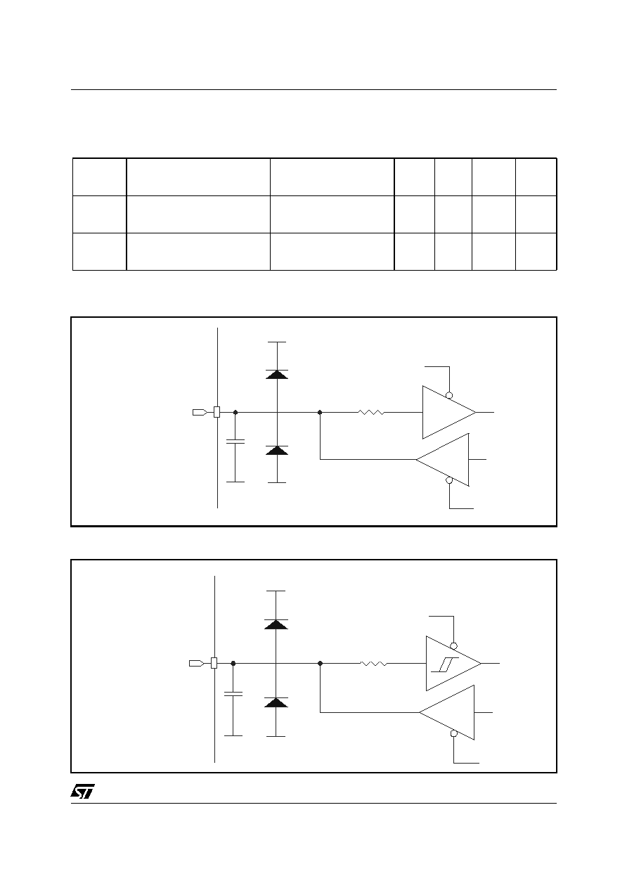
ST52T410/ST52T420/E420
77/84
Subject to general operating condition for V
DD
, f
osc
, and T
A
, unless otherwise specified.
Figure 11.14 Port A and Port C pin Equivalent Circuit
Figure 11.15 Port B Pin Equivalent Circuit
Table 11.12 Output Driving Current
Symbol
Parameter
Test Conditions
Min
Typ
Max
Unit
R
S
Input protection resistor
All input Pins
1
k
C
S
Pin Capacitance
All input Pins
5
pF
V
Input/Output
Device
SS
V
C
S
V
SS
S
R
OUT
V
IN
V
DD
V
V
Device
V
V
V
R
DD
SS
SS
IN
OUT
S
C
S
Input/Output
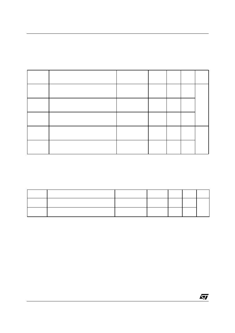
ST52T410/ST52T420/E420
78/84
11.9 Control Pin Characteristics
11.9.1 RESET pin.
Subject to general operating conditions for V
DD
, f
osc
, and T
A,
unless otherwise specified
11.9.2 V
PP
pin.
Subject to general operating conditions for V
DD,
f
osc
, and T
A
,unless otherwise specified.
Notes:
1. Data is based on characterization results, not tested in production.
2. Hysteresis voltage between Schmitt trigger switching level.
Based on characterization results not tested in production.
3. Data is based on design simulation and/or technology characteristics, not tested in production.
4. In working mode V
PP
must be tied to V
SS
Table 11.13 Reset pin
Symbol
Parameter
Conditions
Min
Typ
Max
Unit
V
IL
Input low level voltage
1)
V
DD
= 5 V
0.8
V
V
IH
Input high level voltage
1)
V
DD
= 5 V
2.2
V
hys
Schmitt trigger voltage hysteresis
2)
V
DD
= 5 V
1.4
t
w(RSTL)out
General reset pulse duration
30
µ
S
t
h(RSTL)int
External reset pulse hold time
20
Table 11.14 V
PP
4)
pin
Symbol
Parameter
Conditions
Min
Typ
Max
Unit
V
IL
Input low level voltage
3)
V
SS
0.2
V
V
IH
Input high level voltage
3)
V
DD
-0.1
12.6

ST52T410/ST52T420/E420
79/84
11.10 8-bit A/D Characteristics
Subject to general operating conditions for V
DD
, f
osc
, and T
A
, unless otherwise specified.
Notes:
1. Noise on V
DDA
, V
SSA
< 40 mV
Symbol
Parameter
Conditions
Min
Typ
Max
Unit
Res
Resolution
8
bit
A
TOT
Total Accuracy
1)
1 MHz<f
ADC
< 20 MHz
±
1
LSB
t
C
Conversion Time
82/f
ADC
160/f
ADC
µ
S
V
AN
Conversion Range
V
SSA
V
DDA
V
V
ZI
Zero Scale Voltage
Conversion result =
00 Hex
V
SSA
V
V
FS
Full Scale Voltage
Conversion result =
FF Hex
V
DDA
V
AD
I
Analog Input Current
during Conversion
f
ADC
=20MHz
1
µ
A
AC
IN
Analog Input Capacitance
25
pF
f
ADC
ADC Clock frequency
f
osc
/2
f
osc
MHz

ST52T410/ST52T410/E420
80/84
Table 11.15 PS028 PACKAGE MECHANICAL DATA
DIM
mm
inch.
MIN
TYP.
MAX
MIN
TYP.
MAX
A
2.65
0.104
a1
0.1
0.3
0.004
0.012
b
0.35
0.49
0.014
0.019
b1
0.23
0.32
0.009
0.013
C
0.5
0.020
c1
45∞(typ.)
D
17.7
18.1
0.697
0.713
E
10
10.65
0.394
0.419
e
1.27
0.050
e3
16.51
0.65
F
7.4
7.6
0.291
0.299
L
0.4
1.27
0.016
0.050
S
8∞(max)
1
14
15
28
D
F
e3
e
b
A
L
E
b1
a1
s
C
c1
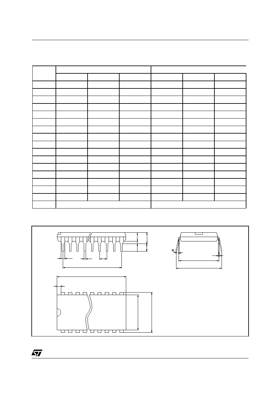
ST52T410/ST52T420/E420
81/84
Table 11.16 Plastic DIP28 PACKAGE MECHANICAL DATA
DIM
mm
inch
MIN
TYP.
MAX
MIN
TYP.
MAX
A
5.08
0.200
A1
0.38
0.015
A2
3.56
4.06
0.140
0.160
B
0.38
0.51
0.015
0.020
B1
1.52
0.060
C
0.20
0.30
0.008
0.012
D
36.83
37.34
1.450
1.470
D2
33.02
1.300
E
15.24
0.600
E1
13.59
13.84
0.535
0.545
e1
2.54
0.100
eA
14.99
0.590
eB
15.24
17.78
0.600
0.700
L
3.18
3.43
0.125
0.135
S
1.78
2.08
0.070
0.082
0∞
10∞
0∞
10∞
N
28
28
1
N
E
1
E
D
S
A
2
A
1
A
D2
B1
B
e1
eB
eA
C

ST52T410/ST52T410/E420
82/84
Table 11.17 CERAMIC DIP28 WINDOWED PACKAGE MECHANICAL DATA
DIM
mm
inch.
MIN
TYP.
MAX
MIN
TYP.
MAX
A
38.10
1.469
B
13.05
13.36
0.514
0.526
C
3.90
5.08
0.153
0.177
D
3.18
0.125
E
0.50
1.78
0.020
0.070
e3
33.02
1.300
F
2.29
2.79
0.90
0.110
G
0.40
0.55
0.18
0.22
I
1.17
1.42
0.48
0.58
L
0.22
0.31
0.010
0.012
M
1.52
2.49
0.060
0.098
N
16.17
18.32
0.637
0.721
N1
4d
15d
P
15.40
15.80
0.606
0.616
Q
5.71
0.225
Diam.
6.86
7.36
0.275
0.285
e3
C
I
G
F
M
E
D
b
A
B
P
L
N
N1
28
1
Diam.
ST52T410/ST52T420/E420
83/84
ORDERING INFORMATION
Each device is available for production in user programmable version (OTP) as well as in factory pro-
grammed version (FASTROM). OTP devices are shipped to the customer with a default blank content
FFh, while FASTROM factory programmed parts contain the code sent by the customer. There is one
common EPROM version for debugging and prototyping, which features the maximum memory size and
peripherals of the family. Care must be taken only to use resources available on the target device.
Figure 11.16 Device Types Selection Guide
PART NUMBER
TEMPERATURE RANGE
PACKAGE
ST52T410G0B6
-40 to +85
∞
C
PDIP
ST52T410G0M6
-40 to +85
∞
C
PSO
ST52T410G1B6
-40 to +85
∞
C
PDIP
ST52T410G1M6
-40 to +85
∞
C
PSO
ST52T410G2B6
-40 to +85
∞
C
PDIP
ST52T410G2M6
-40 to +85
∞
C
PSO
ST52T420G0B6
-40 to +85
∞
C
PDIP
ST52T420G0M6
-40 to +85
∞
C
PSO
ST52T420G1B6
-40 to +85
∞
C
PDIP
ST52T420G1M6
-40 to +85
∞
C
PSO
ST52T420G2B6
-40 to +85
∞
C
PDIP
ST52T420G2M6
-40 to +85
∞
C
PSO
ST52T420G2D6
-40 to +85
∞
C
CDIP
ST52
t
nnn
c m
p
y
TEMPERATURE RANGE:
6 = -40 to 85 ∞C
PACKAGES:
B = PDIP
M = PSO
D = CDIP
MEMORY SIZE:
0 = 1 Kb
1 = 2 Kb
2 = 4 Kb
PIN COUNT:
G = 28 pin
SUBFAMILY:
410, 420
MEMORY TYPE:
T = OTP
E = EPROM
FAMILY

84/84
Full Product Information at http://www.st.com/five
Information furnished is believed to be accurate and reliable. However, STMicroelectronics assumes no responsibility for the consequences
of use of such information nor for any infringement of patents or other rights of third parties which may result from its use. No license is granted
by implication or otherwise under any patent or patent rights of STMicroelectronics. Specification mentioned in this publication are subject to
change without notice. This publication supersedes and replaces all information previously supplied. STMicroelectronics products are not
authorized for use as critical components in life support devices or systems without express written approval of STMicroelectronics.
The ST logo is a registered trademark of STMicroelectronics
© 2002 STMicroelectronics ≠ Printed in Italy ≠ All Rights Reserved
STMicroelectronics GROUP OF COMPANIES
Australia - Brazil - China - Canada - Finland - France - Germany - Hong Kong - India - Israel - Italy - Japan - Malaysia - Malta
- Morocco - Singapore - Spain - Sweden - Switzerland - United Kingdom - U.S.A.
http://www.st.com