 | –≠–ª–µ–∫—Ç—Ä–æ–Ω–Ω—ã–π –∫–æ–º–ø–æ–Ω–µ–Ω—Ç: TD340 | –°–∫–∞—á–∞—Ç—å:  PDF PDF  ZIP ZIP |
1/21
s
QUAD N-CHANNEL MOSFET DRIVE
s
INTEGRATED CHARGE PUMP FOR HIGH
SIDE MOSFET DRIVING
s
VERY LOW GROUND EMI NOISE
s
MOTOR SPEED AND DIRECTION CON-
TROL (LOW SIDE PWM)
s
INTERNAL OR EXTERNAL PWM SOURCE
s
25kHz SWITCHING FREQUENCY ABILITY
s
SYNCHRONOUS HIGH SIDE RECTIFICA-
TION
s
REVERSED BATTERY ACTIVE PROTEC-
TION ABILITY
s
INTEGRATED 5V POWER SUPPLY FOR
MICROCONTROLLER
s
INTEGRATED SECURITY CIRCUITS:
UVLO, OVLO, WATCHDOG
s
60V MAX RATING
DESCRIPTION
The TD340 integrated circuit allows N-Channel
Power
Mosfets
driving
in
a
full
H-bridge
configuration and is best suited for DC Motor
Control Applications. The four drivers outputs are
designed to allow 25kHz MOSFET switching.
The speed and direction of the motor are to be set
by two pins. Voltage across the motor is controlled
by low side Pulse Width Modulation (PWM). This
PWM feature can be made internally when the
input pin is connected to an analog signal, or it can
be given directly from a digital source.
An internal charge pump allows proper upper
MOS driving for full static operation (100% PWM).
TD340 achieves very low EMI noise thanks to its
balanced charge pump structure and its drivers
moderate slew rate.
To avoid excessive heating due to free wheeling,
appropriate synchronous rectification is achieved
on the corresponding High Side MOSFET.
Moreover,
TD340
integrates
a
5V
voltage
regulator suitable as a power supply output for the
microcontroller, a Reset circuit and a Watchdog
circuit.
Security functions disable the TD340 (MOS off)
when abnormal conditions occur like overvoltage,
undervoltage or CPU loss of control (watchdog).
TD340 withstands transients as met in automotive
field without special protection devices thanks to
its 60V BCD technology.
ORDER CODE
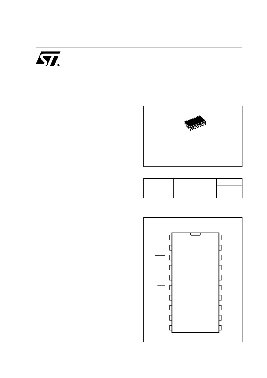
D = Small Outline Package (SO) - also available in Tape & Reel (DT)
PIN CONNECTIONS (top view)
Part Number
Temperature Range
Package
D
TD340ID
-40
∞
C, +125
∞
C
∑
D
SO20
(Plastic Micropackage)
VBATT
VOUT
RESET
CWD
WD
STBY
TEMP
IN1
IN2
CF
GND
L1
L2
S2
H2
CB2
S1
H1
CB1
OSC
10
9
8
7
6
5
4
3
2
1
11
12
13
14
15
16
17
18
19
20
TD340
H-BRIDGE QUAD POWER MOSFET DRIVER
FOR DC MOTOR CONTROL
This is preliminary information on a new product now in development or undergoing evaluation. Details are subject to change without notice.
May 2000
PRELIMINARY DATA
TD340
2/21
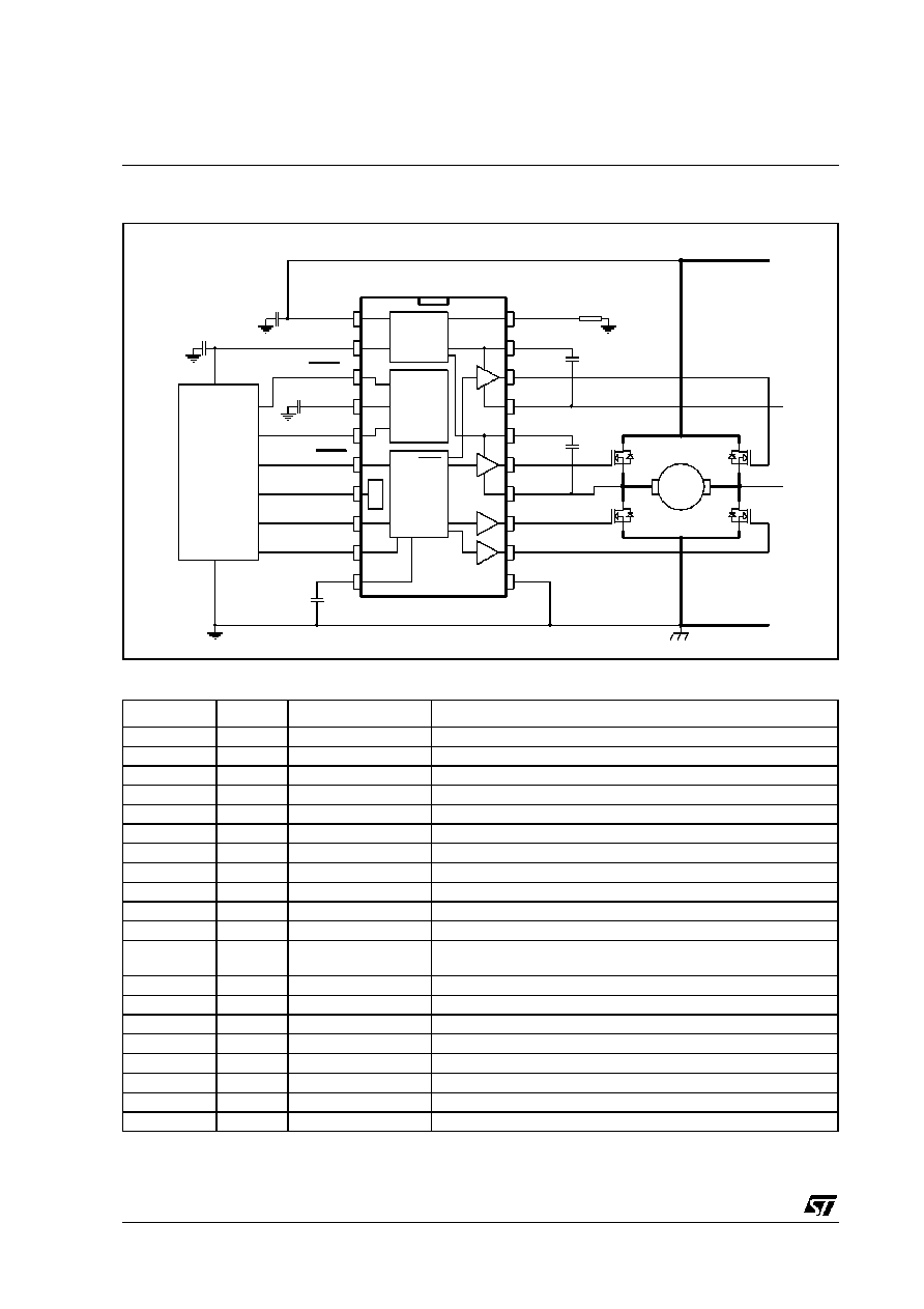
SYSTEM AND INTERNAL BLOCK DIAGRAM
PIN DESCRIPTION
VBATT
VOUT
RESET
CWD
WD
STBY
TEMP
IN1
IN2
CF
GND
L1
L2
S2
H2
CB2
S1
H1
CB1
OSC
Q2H
Q2L
Q1H
Q1L
BATT -
BATT +
T
∞
LOGIC
PWM
PWM
WATCHDOG
RESET
SUPPLY
UVLO
OVLO
TD340
µ
CONTROLLER
5V
0V
M
Name
Pin
Type
Function
VBATT
1
Power Input
Power Supply
GND
11
Ground
Ground
L1
12
Push Pull Output
Low Side Drive - Gate 1
L2
13
Push Pull Output
Low Side Drive - Gate 2
H1
18
Push Pull Output
High Side Drive - Gate 1
H2
15
Push Pull Output
High Side Drive - Gate 2
S1
17
Analog Input
High Side Drive - Source 1
S2
17
Analog Input
High Side Drive - Source 2
CB1
19
Analog Input
High Side Drive - Bootstrap Capacitor 1
CB2
16
Analog Input
High Side Drive - Bootstrap Capacitor 2
CF
10
Analog Input
External Capacitor to set the PWM Switching Frequency
IN1
8
Analog or Digital Input
Analog Level of PWM (0 to 100%) if CF connected to a capacitor,
or PWM Signal if CF connected to ground
IN2
9
Digital Input
Direction to the Motor's Rotation
STBY
6
Digital Input
Standby Mode
TEMP
7
Analog Output
Analog Indicator of Temperature
VOUT
2
Power Output
Regulated Power Supply Output for the Microcontroller - 5V
RESET
3
Open Drain Output
Reset Signal for the Microcontroller
WD
5
Digital Input
Watchdog Signal from the
icrocontroller
CWD
4
Analog Input
External Capacitor to set Watchdog Timeout
OSC
20
Digital Output
Oscillator Output

TD340
3/21
ABSOLUTE MAXIMUM RATINGS
Notes:
1. The duration of the 60V voltage must be limited to 1 second if current is drained from the Vout regulator. Supply voltage in steady state
must be limi ted to ensure that dissipation rating is not exceeded.
2. The magnitude of input and output voltages must never exceed Vbatt+0.3V or 60V, whichever is less, except for H1 and H2: Vbatt+15V
or 60V, whichever is less.
OPERATING CONDITIONS
Symbol
Parameter
Value
Unit
V
Batt
Positive Supply Voltage - Note 1
60
V
P
d
Power Dissipation
500
mW
T
stg
Storage Temperature
-55 to +150
o
C
ESD
Electrostatic Discharge
2
kV
V
digital
Voltage on pins: IN1, IN2, STBY, WD, CWD, CF, TEMP, VOUT,
RESET
-0.3 to 7
V
V
lowgate
Voltage on pins: L1, L2
-0.3 to 15
V
V
power
Voltage on pins: H1, H2, S1, S2, CB1, CB2 - Note 2
-0.3 to 60
V
V
osc
Voltage on pin OSC
Vbatt-6.5 to Vbatt
V
T
j
Maximum Junction Temperature
150
∞
C
R
hja
Thermal Resistance Junction-Ambient
85
∞
C/W
Symbol
Parameter
Value
Unit
V
batt
Positive Supply Voltage
6.5 to 18.5
V
T
oper
Operating Free Air Temperature Range
-40 to +125
∞
C

TD340
4/21
ELECTRICAL CHARACTERISTICS
Vbatt= 12V, Tamb=-40
∞
C to 125
∞
C (unless otherwise specified)
Symbol
Parameter
Test Condition
Min.
Typ.
Max.
Unit
I
CC
Total Supply Current
T
min.
< T
amb
< T
max.
T=25
∞
C
-40
∞
C < T < 125
∞
C
4.5
5
7
10
mA
mA
I
stdby
Supply Current in Standby Mode
T=25
∞
C
-40
∞
C < T < 125
∞
C
180
300
350
µ
A
µ
A
Standby
H
STDBY Pin Voltage for Standby OFF
0.8
V
Standby
L
STDBY Pin Voltage for Standby ON
2
V
UVLO
Under Voltage Lockout - when
Vbatt<UVLO all buffer outputs are low
Vbatt decreasing
Hyst. = 100mV typ.
5.8
6.2
6.5
V
OVLO
Under Voltage Lockout - when
Vbatt>OVLO all buffer outputs are low
Vbatt decreasing
Hyst. = 300mV
18.5
20
21.5
V
DRIVERS - Cbootstrap=47nF
V
gs
Static Gate-Source High Side Mosfet Volt-
age (charge pump)
No Bootstrap Cap
8
11
15
V
V
gsd
Dynamic Gate-Source High Side Mosfet
Voltage (bootstrap)
9
V
Freq
Switching Frequency of PWM
Cf = 270pF
20
25
30
kHz
t
d
Dead Time for secure Synchronous
Rectification
Cf=270nF, IN1=2.4V
No Load
Cload=4nF
2.1
2.8
1.5
3.5
µ
s
µ
s
I
outl
Output Current Capability - Low Side
Source
Sink
T=25
∞
C
40
∞
C < T < 125
∞
C
T=25
∞
C
40
∞
C < T < 125
∞
C
30
25
60
50
50
50
100
100
100
100
150
150
mA
mA
mA
mA
I
outh
Output Current Capability - High Side
Source
Sink
T=25
∞
C
40
∞
C < T < 125
∞
C
T=25
∞
C
40
∞
C < T < 125
∞
C
30
25
60
50
50
50
100
100
100
100
150
150
mA
mA
mA
mA
OSCILLATOR - Rosc=5.6k - Note 1
F
osc
Frequency of internal Step up converter
Oscillator
T=25
∞
C
40
∞
C < T < 125
∞
C
0.6
0.5
1
1
1.4
1.5
MHz
MHz
V
osc
Oscillator Swing - note 7
Vbatt = 12V
Vbatt = 9V
Vbatt > UVLO
6.25
6.25
5.1
12
12
12.5
V
V
V

TD340
5/21
ELECTRICAL CHARACTERISTICS (continued)
Vbatt= 12V, Tamb=-40
∞
C to 125
∞
C (unless otherwise specified)
Symbol
Parameter
Test Conditio n
Min.
Typ.
Max.
Unit
VOLTAGE REGULATOR - Co=220nF - note 2
V
out
Output Voltage
Io=20mA
T=25
∞
C
40
∞
C < T < 125
∞
C
4.6
4.5
5
5
5.4
5.5
V
V
Line
Reg
Line Regulation
6V < Vbatt < 16V, Io=20mA
T=25
∞
C
40
∞
C < T < 125
∞
C
100
150
mV
mV
Load
Reg
Load Regulation
0
Io
40mA
T=25
∞
C
40
∞
C < T < 125
∞
C
20
40
mV
mV
I
o
Maximum Output Current
Vbatt = 12V
6V < Vbatt < 16V
40
20
mA
mA
I
os
Output Current Short Circuit
Vout=0
100
200
mA
RESET SUPERVISORY CIRCUIT - note 3
Vt
hi
Threshold Voltage Vout Increasing
T=25
∞
C
40
∞
C < T < 125
∞
C
4.0
3.9
4.3
4.5
4.6
V
V
V
thd
Threshold Voltage Vout Decreasing
T=25
∞
C
40
∞
C < T < 125
∞
C
3.9
3.8
4.2
4.4
4.5
V
V
k
i
Linearity coefficient (Vthi = ki Vout)
0.86
k
d
Linearity coefficient (Vthd = kd Vout)
0.84
V
hys
Hysteresis Threshold Voltage
50
100
200
mV
t
phl
Response Time High to Low
5
µ
s
WATCHDOG CIRCUIT
t
wd
Watchdog Time Out Period
No ext. capacitor
Cwd = 47nF - note 4
0.5
0.7
1
1
2
1.5
ms
s
t
ipw
Watchdog Input Pulse Width for Proper
Retrigger
0.1
µ
s
t
ipr
Watchdog Input Rise Time for Proper
Retrigger
0.1
µ
s
t
reset
Reset Pulse Width
10
20
40
µ
s
TEMPERATURE OUTPUT
V
T
Output Voltage
T= 25
o
C
2.58
2.68
2.78
V
V
T
Output Temperature Drift
-7
-7.5
-7.8
mV/
o
C
Notes :
1. For proper operation, a 5.6k resistor needs to be connected between OSC and GND.
2. 220nF is the optimized value for the voltage regulator
3. The reset thresholds (Vout increasing and decreasing) are proportional to Vout, (coefficients ki and kd). ki and kd vary in the same direc-
tion with temperature.
4. Watchdog capacitor Cwd should be placed as close as possible to CWD pin.