 | –≠–ª–µ–∫—Ç—Ä–æ–Ω–Ω—ã–π –∫–æ–º–ø–æ–Ω–µ–Ω—Ç: TDA2003 | –°–∫–∞—á–∞—Ç—å:  PDF PDF  ZIP ZIP |
Æ
TDA2003
10W CAR RADIO AUDIO AMPLIFIER
DESCRIPTION
The TDA 2003 has improved performance with the
same pin configuration as the TDA 2002.
The additional features of TDA 2002, very low
number of external components,ease of assembly,
space and cost saving, are maintained.
The device provides a high output current capability
(up to 3.5A) very low harmonic and cross-over
distortion.
Completely safe operation is guaranteed due to
protectionagainst DC and AC short circuit between
all pins and ground, thermal over-range, load dump
voltage surge up to 40V and fortuitous open
ground.
October 1998
Symbol
Parameter
Value
Unit
V
S
Peak supply voltage (50ms)
40
V
V
S
DC supply voltage
28
V
V
S
Operating supply voltage
18
V
I
O
Output peak current (repetitive)
3.5
A
I
O
Output peak current (non repetitive)
4.5
A
Ptot
Power dissipation at Tcase = 90
∞
C
20
W
T
stg
, T
j
Storage and junction temeperature
-40 to 150
∞
C
ABSOLUTE MAXIMUM RATINGS
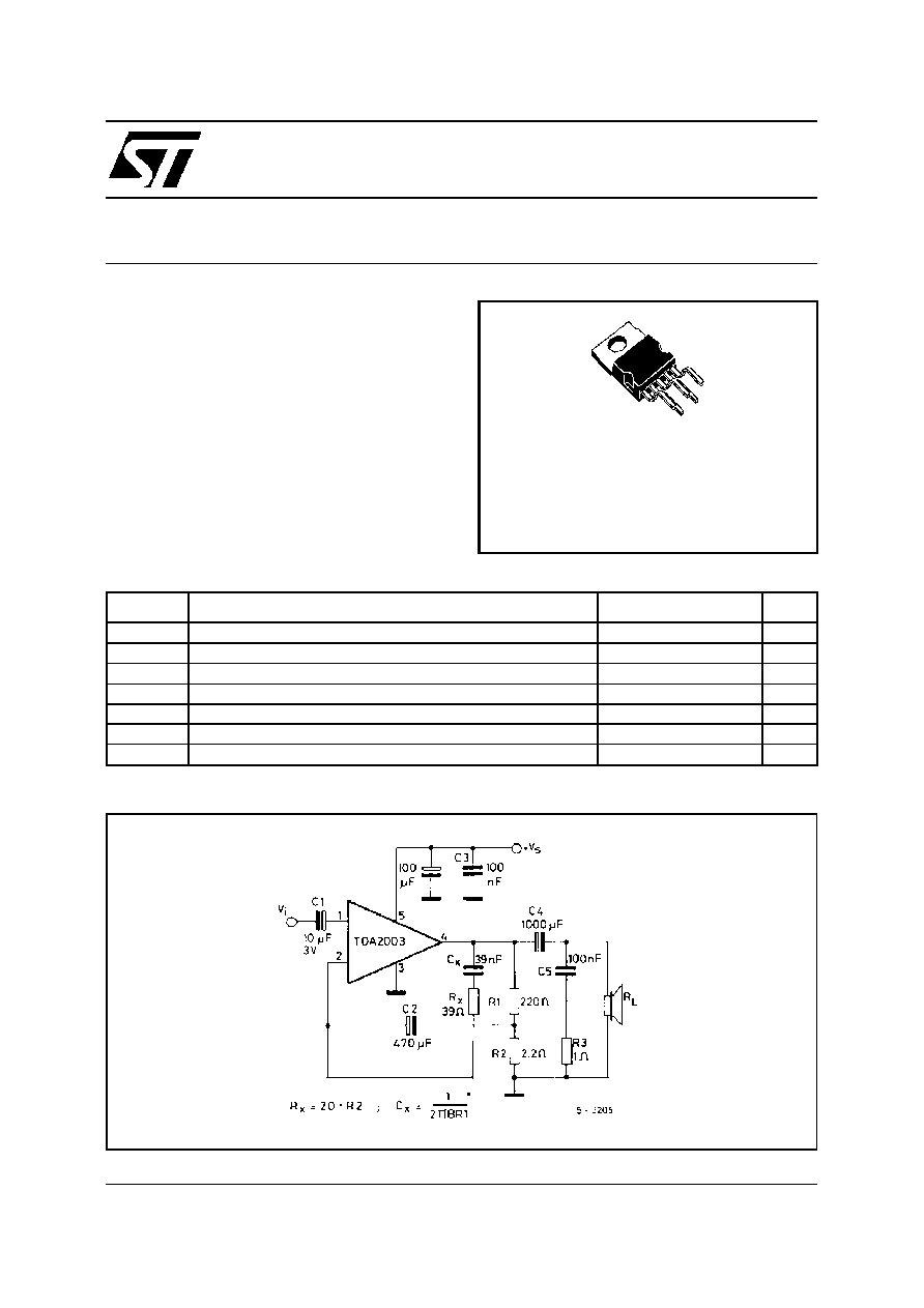
TEST CIRCUIT
PENTAWATT
ORDERING NUMBERS : TDA 2003H
TDA 2003V
1/10
Symbol
Parameter
Value
Unit
R
th-j-case
Thermal resistance junction-case
max
3
∞
C/W
THERMAL DATA
2/10
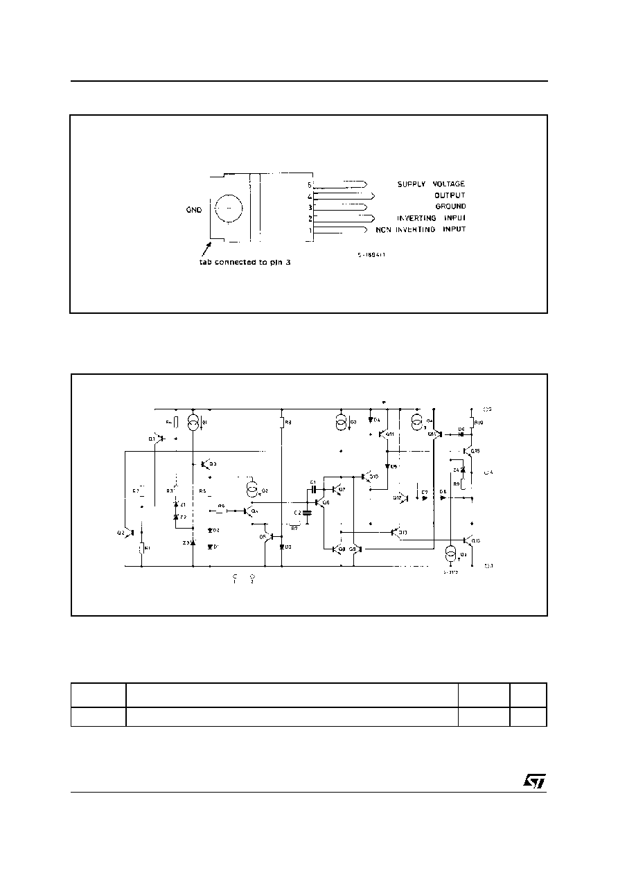
PIN CONNECTION (top view)
SCHEMATIC DIAGRAM
TDA2003
Symbol
Parameter
Test conditions
Min.
Typ.
Max.
Unit
DC CHARACTERISTICS (Refer to DC test circuit)
V
s
Supply voltage
8
18
V
V
o
Quiescent output voltage (pin 4)
6.1
6.9
7.7
V
I
d
Quiescent drain current (pin 5)
44
50
mA
AC CHARACTERISTICS (Refer to AC test circuit, Gv = 40 dB)
P
o
Output power
d = 10%
f = 1 kHz
R
L
= 4
R
L
= 2
R
L
= 3.2
R
L
= 1.6
5.5
9
6
10
7.5
12
W
W
W
W
V
i(rms)
Input saturation voltage
300
mV
V
i
Input sensitivity
f = 1 kHz
P
o
= 0.5W
P
o
= 6W
P
o
= 0.5W
P
o
10W
R
L
= 4
R
L
= 4
R
L
= 2
R
L
= 2
14
55
10
50
mV
mV
mV
mV
ELECTRICAL CHARACTERISTICS ( V
s
= 14.4V, T
amb
= 25
∞
C unless otherwise specified)
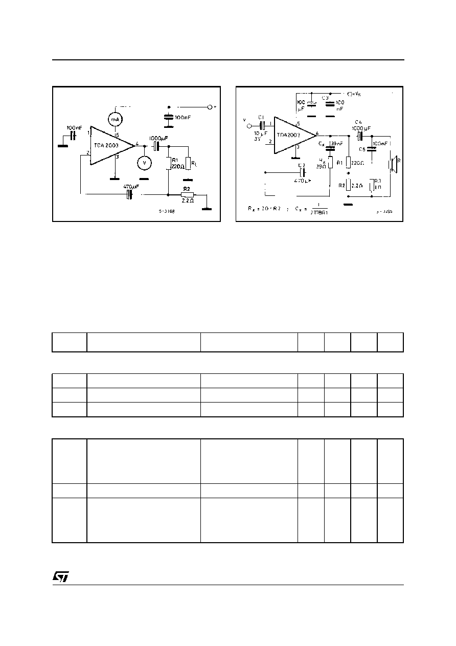
DC TEST CIRCUIT
AC TEST CIRCUIT
3/10
TDA2003
4/10
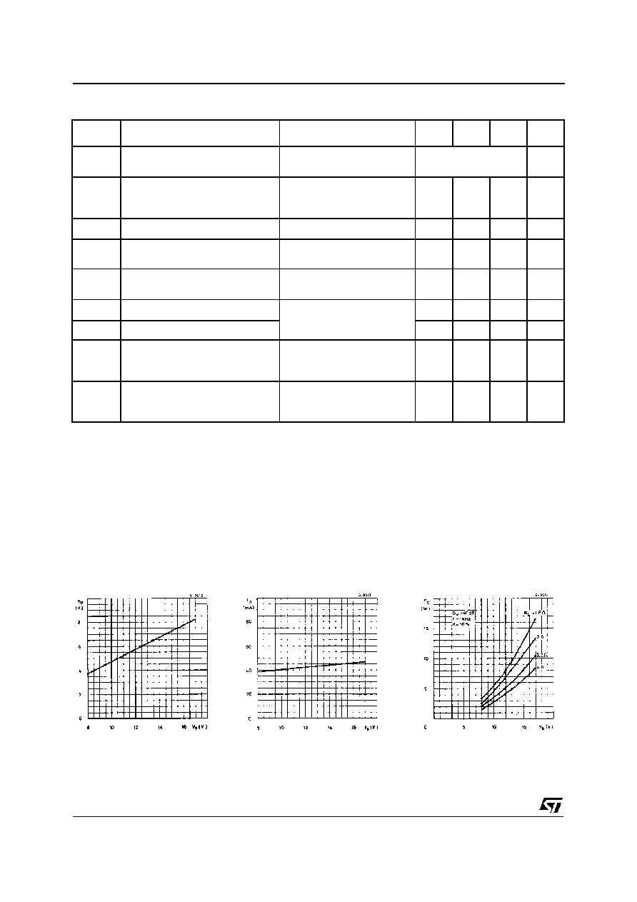
Figure 1. Quiescent output
voltage vs. supply voltage
Figure 2. Quiescent drain
current vs. supply voltage
Figure 3. Output power vs.
supply voltage
Symbol
Parameter
Test conditions
Min.
Typ.
Max.
Unit
B
Frequency response (-3 dB)
P
o
= 1W
R
L
= 4
40 to 15,000
Hz
d
Distortion
f = 1 kHz
P
o
= 0.05 to4.5W R
L
= 4
P
o
= 0.05 to 7.5W R
L
= 2
0.15
0.15
%
%
R
i
Input resistance (pin 1)
f = 1 kHz
70
150
k
G
v
Voltage gain (open loop)
f = 1 kHz
f = 10 kHz
80
60
dB
dB
G
v
Voltage gain (closed loop)
f = 1 kHz
R
L
= 4
39.3
40
40.3
dB
e
N
Input noise voltage
(0)
1
5
µ
V
i
N
Input noise current
(0)
60
200
pA
Efficiency
f = 1 Hz
P
o
= 6W
P
o
= 10W
R
L
= 4
R
L
= 2
69
65
%
%
SVR
Supply voltage rejection
f = 100 Hz
V
ripple
= 0.5V
R
g
= 10 k
R
L
= 4
30
36
dB
ELECTRICAL CHARACTERISTICS (continued)
(0) Filter with noise bandwidth: 22 Hz to 22 kHz
TDA2003

Figure 4. Output power vs.
load resistance R
L
Fi gure 5. Gain vs. inp ut
sensivity
Figure 6. Gain vs. input
sensivity
F i gu re 7. Di st ort ion vs.
output power
Fi g ure 8. D isto r tion vs.
frequency
Figure 9. Supply voltage
rejection vs. voltage gain
Figure 10. Supply voltage
rejection vs. frequency
Figure 11. Power dissipa-
tion and efficiency vs. output
power (R
L
= 4
)
Figure 12. Powe r dissipa-
tion and efficiencyvs. output
power (R
L
= 2
)
5/10
TDA2003