 | –≠–ª–µ–∫—Ç—Ä–æ–Ω–Ω—ã–π –∫–æ–º–ø–æ–Ω–µ–Ω—Ç: TDA2052H | –°–∫–∞—á–∞—Ç—å:  PDF PDF  ZIP ZIP |
TDA2052
60W Hi-Fi AUDIO POWER AMPLIFIER
WITH MUTE / STAND-BY
SUPPLY VOLTAGE RANGE UP TO
±
25V
SPLIT SUPPLY OPERATION
HIGH OUTPUT POWER
(UP TO 60W MUSIC POWER)
LOW DISTORTION
MUTE/STAND-BY FUNCTION
NO SWITCH ON/OFF NOISE
AC SHORT CIRCUIT PROTECTION
THERMAL SHUTDOWN
ESD PROTECTION
DESCRIPTION
The TDA2052 is a monolithic integrated circuit in
Heptawatt package, intended for use as audio
class AB amplifier in TV or Hi-Fi field application.
Thanks to the wide voltage range and to the high
out current capability it's able to supply the high-
est power into both 4
and 8
loads even in
presence of poor supply regulation.
The built in Muting/Stand-by function simplifies
the remote operations avoiding also switching on-
off noises.
This is advanced information on a new product now in development or undergoing evaluation. Details are subject to change without notice.
January 2003
Æ
Heptawatt V Heptawatt H
ORDERING NUMBERS:
TDA2052V TDA2052H
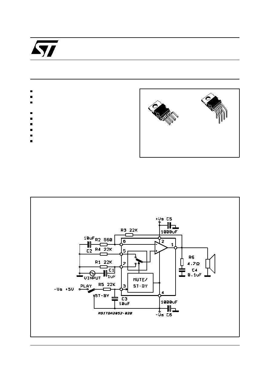
TEST AND APPLICATION CIRCUIT
1/14
ABSOLUTE MAXIMUM RATINGS
Symbol
Parameter
Value
Unit
V
S
DC Supply Voltage
±
25
V
I
O
Output Peak Current (internally limited)
6
A
P
tot
Power Dissipation T
case
= 70
∞
C
30
W
T
op
Operating Temperature Range
0 to +70
∞
C
T
stg
, T
j
Storage and Junction Temperature
-40 to +150
∞
C
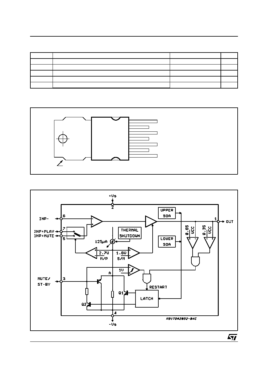
BLOCK DIAGRAM
1
2
3
4
5
6
7
NON INVERTING INPUT(PLAY)
INVERTING INPUT
-V
S
STAND-BY/MUTE
+V
S
OUTPUT
D95AU326
tab connected to pin 4
NON INVERTING INPUT(MUTE)
PIN CONNECTION (Top view)
TDA2052
2/14

ELECTRICAL CHARACTERISTICS (Refer to the test circuit, G
V
= 32dB; V
S
+ 18V; f = 1KHz; T
amb
=
25
∞
C, unless otherwise specified.)
Symbol
Parameter
Test Condition
Min.
Typ.
Max.
Unit
V
S
Supply Range
+6
+25
V
I
q
Total Quiescent Current
V
S
= +22V
20
40
70
mA
I
b
Input Bias Current
+0.5
µ
A
V
OS
Input Offset Voltage
+15
mV
I
OS
Input Offset Current
+200
nA
P
O
Music Output Power
IEC268-3 Rules (*)
V
S
= + 22.5, R
L
= 4
,
d = 10%, t = 1s
50
60
W
P
O
Output Power (continuous RMS)
d = 10%
RL = 4
R
L
= 8
V
S
= +22V, R
L
= 8
35
30
40
22
33
W
W
W
d = 1%
R
L
= 4
R
L
= 8
V
S
= +22V, R
L
= 8
32
17
28
W
W
W
d
Total Harmonic Distortion
R
L
= 4
P
O
= 0.1 to 20W;
f = 100Hz to 15KHz
V
S
+ 22V, R
L
= 8
P
O
= 0.1 to 20W;
f = 100Hz to 15KHz
0.1
0.1
0.7
0.5
%
%
SR
Slew Rate
3
5
V/
µ
s
G
V
Open Loop Voltage Gain
80
dB
e
N
Total Input Noise
A Curve
f = 20Hz to 20KHz
2
3
10
µ
V
µ
V
R
i
Input Resistance
500
K
SVR
Supply Voltage Rejection
f = 100Hz, V
ripple
= 1V
RMS
40
50
dB
T
S
Thermal Shutdown
145
∞
C
MUTE/STAND-BY FUNCTION (Ref. ≠V
S
)
VT
ST-BY
Stand-by - Threshold
1
1.8
V
VT
PLAY
Play Threshold
2.7
4
V
I
q ST-BY
Quiescent Current @ Stand-by
V
pin 3
= 0.5V
1
3
mA
ATT
ST-BY
Stand-by Attenuation
70
90
dB
I
pin3
Pin 3 Current @ Stand-by
≠1
+10
µ
A
Note (*):
MUSIC POWER CONCEPT
MUSIC POWER is ( according to the IEC clauses n.268-3 of Jan 83) the maximal power which the amplifier is capable of producing across the
rated load resistance (regardless of non linearity) 1 sec after the application of a sinusoidal input signal of frequency 1KHz.
According to this definition our method of measurement comprises the following steps:
1) Set the voltage supply at the maximum operating value -10%
2) Apply a input signal in the form of a 1KHz tone burst of 1 sec duration; the repetition period of the signal pulses is > 60 sec
3) The output voltage is measured 1 sec from the start of the pulse
4) Increase the input voltage until the output signal show a THD = 10%
5) The music power is then V
2
out
/R1
,
where V
out
is the output voltage measured in the condition of point 4) and R1 is the rated load impedance
The target of this method is to avoid excessive dissipation in the amplifier.
THERMAL DATA
Symbol
Description
Value
Unit
R
th j-case
Thermal Resistance Junction-case
Max
2.5
∞
C/W
TDA2052
3/14
APPLICATIONS SUGGESTIONS (See Test and Application Circuit)
The recommended values of the external components are those shown on the application circuit. Differ-
ent values can be used; the following table can help the designer.
Comp.
Value
Purpose
Larger Than
Smaller Than
R1
22K
(*)
Input Impedance
Increase of Input
Impedance
Decrease of Input
Impedance
R2
560
Closed Loop Gain set to
32dB (**)
Decrease of Gain
Increase of Gain
R3
22K
(*)
Increase of Gain
Decrease of Gain
R4
22K
(*)
Input Impedance @ Mute
R5
22K
Stand-by Time Constant
R6
4.7
Frequency Stability
Danger of oscillations
Danger of oscillations
C1
1
µ
F
Input DC Decoupling
Higher Low-frequency
cut-off
C2
10
µ
F
Feedback DC Decoupling
Higher Low-frequency
cut-off
C3
10
µ
F
Stand-by Time Constant
C4
0.100
µ
F
Frequency Stability
Danger of Oscillations
C5, C6
1000
µ
F
Supply Voltage Bypass
(*) R1 = R3 = R4 for POP optimization
(**) Closed Loop Gain has to be
30dB
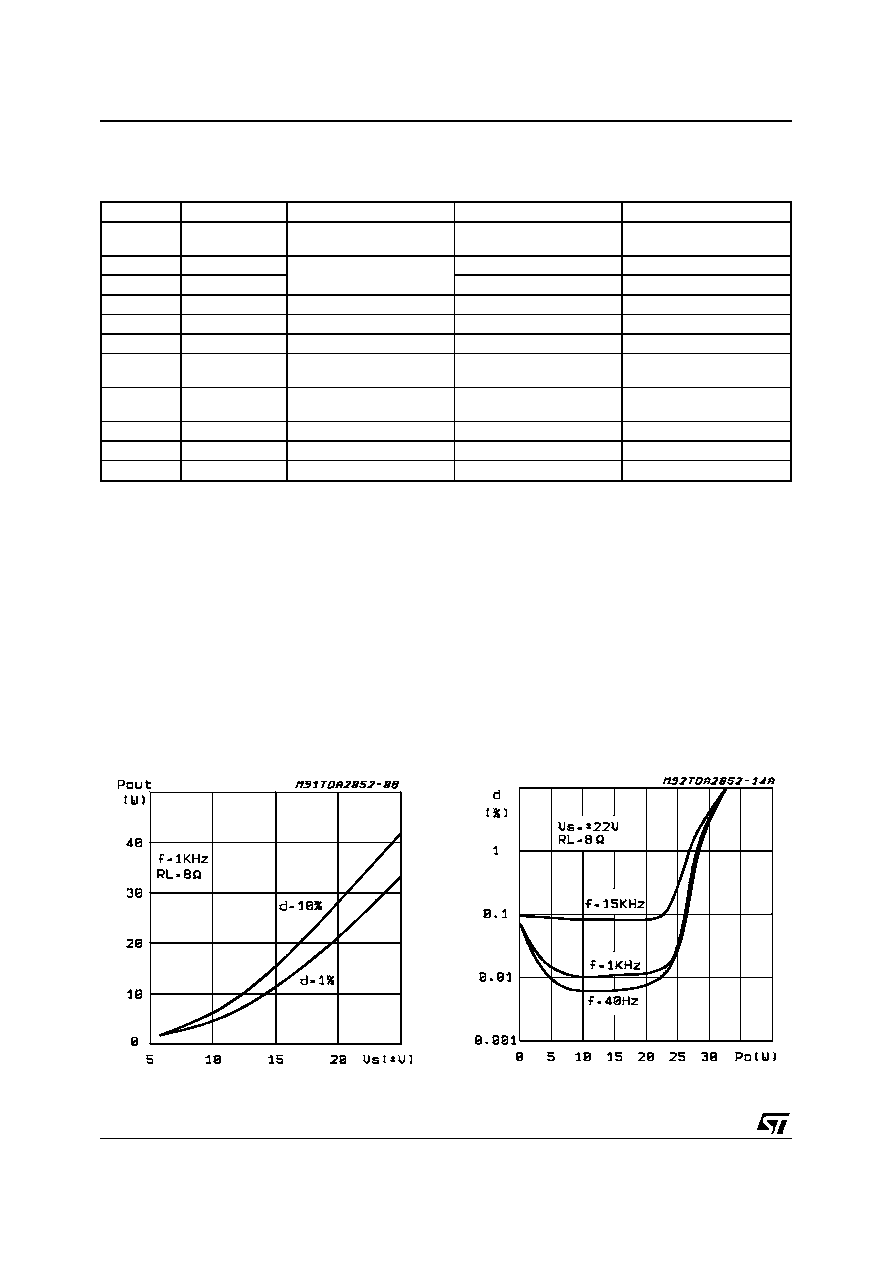
Figure 1: Output Power vs. Supply Voltage
Figure 2: Distortion vs. Output Power
TYPICAL CHARACTERISTICS
TDA2052
4/14
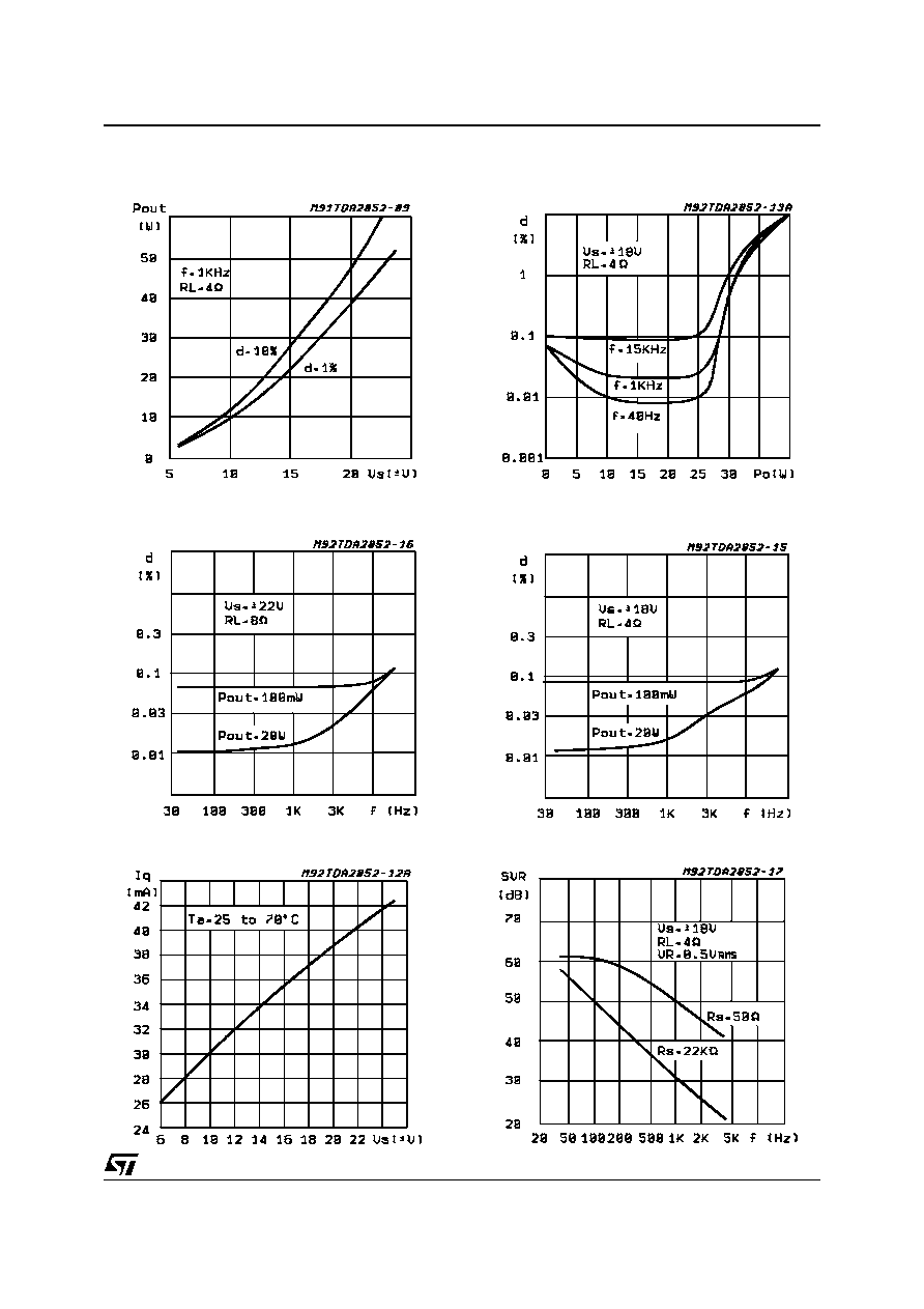
Figure 3: Output Power vs. Supply Voltage.
Figure 4: Distortion vs. Output Power.
Figure 5: Distortion vs. Frequency.
Figure 6: Distortion vs. Frequency.
Figure 7: Quiescent Current vs. Supply Voltage
Figure 8: Supply Voltage Rejection vs. Frequency.
TDA2052
5/14