 | –≠–ª–µ–∫—Ç—Ä–æ–Ω–Ω—ã–π –∫–æ–º–ø–æ–Ω–µ–Ω—Ç: TDA2170 | –°–∫–∞—á–∞—Ç—å:  PDF PDF  ZIP ZIP |
TDA2170
TV VERTICAL DEFLECTION OUTPUT CIRCUIT
December 1992
11
10
9
8
7
6
5
4
3
2
1
Tab connected to Pin 6
NC
GND
REFERENCE VOLTAGE
OUTPUT STAGE SUPPLY
OUTPUT
GND
FLYBACK GENERATOR
SUPPLY VOLTAGE
NON INVERTING INPUT
INVERTING INPUT
NC
2170-01.EPS
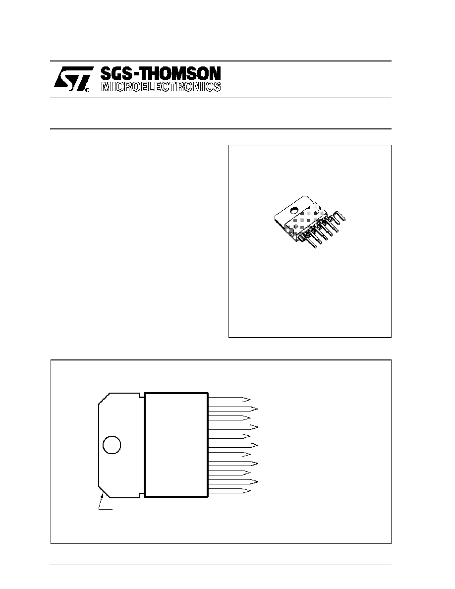
PIN CONNECTIONS
MULTIWATT 11
(Plastic Package)
ORDER CODE : TDA2170
The functions incorporated are :
.
POWER AMPLIFIER
.
FLYBACK GENERATOR
.
REFERENCE VOLTAGE
.
THERMAL PROTECTION
DESCRIPTION
The TDA2170 is a monolithic integrated circuit in
11-lead Multiwatt
Æ
package. It is a high efficiency
power booster for direct driving of vertical windings
of TV yokes. It is intended for use in Colour are B
& W television receivers as well as in monitors and
displays.
1/7

Thermal
P rotect ion
5
8
4
2
3
7
6
YOKE
+V
S
Power
A mplif ier
10
9
Reference
Volt age
Fly back
Generator
2170-02.EPS
BLOCK DIAGRAM
Q11
Q12
D4
D5
R5
R4
Q10
D3
Q9
D6
D7
Q14
Q13
Q15
R7
R6
Q7
Q6
Q8
R3
C2
Q4
C1
Q1
Q2
Q5
Q3
R2
D2
R1
R14
Q26
R17
R18
Q27
R12
Q29
Q28
Z2
D1
R16
R13
Q24
Q25
Q23
Z1
R15
2
3
6
10
9
Q16
R8
R9
Q19
D8
Q17
Q18
Q22
R11
Q20
D9
R12
Q21
7
4
8
5
2170-03.EPS
SCHEMATIC DIAGRAM
TDA2170
2/7
ABSOLUTE MAXIMUM RATINGS
Symbol
Parameter
Value
Unit
V
s
Supply Voltage (pin 4)
35
V
V
7
, V
8
Flyback Peak Voltage
60
V
V
5
Voltage at Pin 5
+ V
s
V
2
, V
3
Amplifier Input Voltage
+ V
s
≠ 0.5
V
I
o
Output Peak Current (non repetitive, t = 2 msec)
2.5
A
I
o
Output Peak Current at f = 50 Hz, t
10
µ
sec
3
A
I
o
Output Peak Current at f = 50 Hz, t > 10
µ
sec
2
A
I
5
Pin 5 DC Current at V
7
< V
4
100
mA
I
5
Pin 5 Peak to Peak Flyback Current at f = 50 Hz, t
fly
1.5 msec
3
A
P
tot
Total Power Dissipation at T
case
= 60
∞
C
30
W
T
stg
, T
j
Storage and Junction Temperature
≠ 40 to 150
∞
C
2170-01.TBL
THERMAL DATA
Symbol
Parameter
Value
Unit
R
th (j-c)
Thermal Resistance Junction-case
Max
3
∞
C/W
R
th (j-a)
Thermal Resistance Junction≠ambient
Max
40
∞
C/W
2170-02.TBL
ELECTRICAL CHARACTERISTICS
(refer to the test circuits, V
S
= 35 V, T
amb
= 25
∞
C unless otherwise specified)
Symbol
Parameter
Test Conditions
Min.
Typ.
Max.
Unit
Fig.
I
4
Pin 4 Quiescent Current
I
5
= 0 ; I
7
= 0 ; V
3
= 3 V
8
16
mA
1a
I
8
Pin 8 Quiescent Current
I
5
= 0 ; I
7
= 0 ; V
3
= 3 V
16
36
mA
1a
I
3
Amplifier Input Bias Current
V
3
= 1 V
≠ 0.1
≠ 1
µ
A
1a
I
2
Amplifier Input Bias Current
V
2
= 1 V
≠ 0.1
≠ 1
µ
A
1a
V
9
Reference Voltage
I
9
= 0
2.2
V
1a
V
9
V
S
Reference Voltage Drift vs. Supply Voltage
V
S
= 15 to 30 V
1
2
mV/V
1a
V
5L
Pin 5 Saturation Voltage to GND
I
5
= 20 mA
1
V
1c
V
7
Quiescent Output Voltage
V
S
= 35 V ; R
a
= 13 k
18
V
1d
V
S
= 15 V ; R
a
= 13 k
7.5
V
1d
V
7L
Output Saturation Voltage to GND
I
7
= 1.2 A
1
1.4
V
1c
I
7
= 0.7 A
0.7
1
V
1c
V
7H
Output Saturation Voltage to Supply
≠ I
7
= 1.2 A
1.6
2.2
V
1b
≠ I
7
= 0.7 A
1.3
1.8
V
1b
R
9
Reference Voltage Output Resistance
2.1
k
T
j
Junction Temperature for Thermal Shut
Down
140
∞
C
2170-03.TBL
TDA2170
3/7

Figure 1 : DC Test Circuits
2170-04.EPS
S
1
: (a) I
2
; (b) I
3
, I
4
and I
8
.
S
2
: (a) I
4
and I
8
; (b) I
3
; (c) I
2
.
S
3
: (a) I
2
, I
3
, I
4
, I
8
, I
9
and V
9
; (b) R9.
Figure 1a : Measurement of I
2
; I
3
; I
4
; I
8
; I
9
;
V
9
/
V
S
; R9
2170-05.EPS
Figure 1b : Measurement of V7
H
2170-06.EPS
S1 : (a) V
5L
; (b) V
7L
.
Figure 1c : Measurement of V
5L
, V
7.L
.
2170-07.EPS
Figure 1d : Measurement of V
7
.
2170-08.EPS
Figure 2 : Application Circuit
TDA2170
4/7
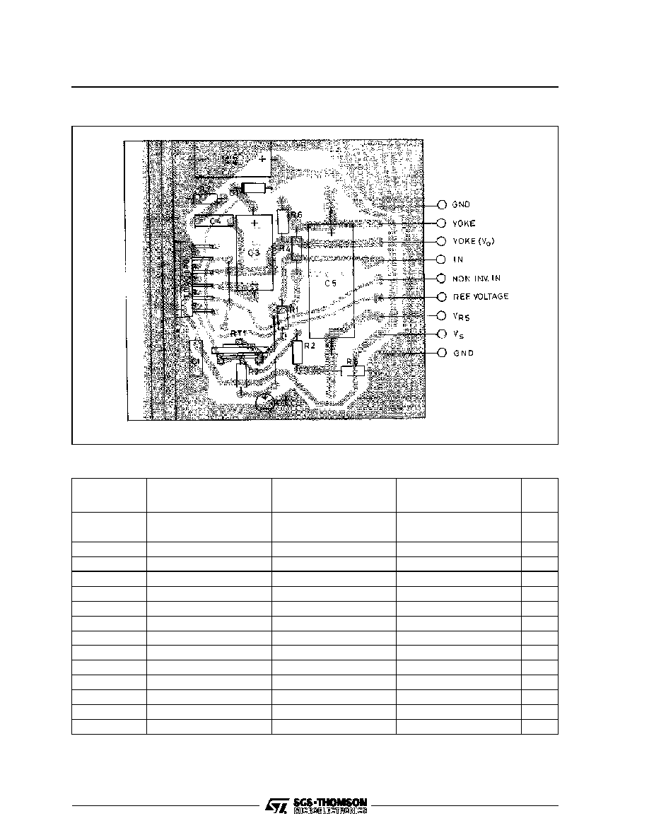
COMPONENTS LIST FOR TYPICAL APPLICATIONS
Component
110
∞
TVC
5.9
/ 10 mH
1.95 App
110
∞
TVC
9.6
/ 24.6 mH
1.2 App
90
∞
TVC
15
/ 30 mH
0.82 App
Unit
RT1
10
4.7
10
k
R1
12
10
12
k
R2
10
5.6
5.6
k
R3
27
12
18
k
R4
12
8.2
5.6
k
R5
0.82
1
1
R6
270
330
330
R7
1.5
1.5
1.5
D1
1N 4001
1N 4001
1N 4001
≠
C1
0.1
0.1
0.1
µ
F
C2 el.
1000/25 V
470/25 V
470/25 V
µ
F
C3 el.
220/25 V
220/25 V
220/25 V
µ
F
C4
0.22
0.22
0.22
µ
F
C5 el.
2200/25 V
2200/25 V
1000/16 V
µ
F
C6 el.
4.7/16 V
4.7/16 V
10/16 V
µ
F
2170-04.TBL
2170-09.TIF
Figure 3 : PC Board and Component Layout (1:1 scale)
TDA2170
5/7
TYPICAL PERFORMANCES
Parameter
110
∞
TVC
5.9
/ 10 mH
110
∞
TVC
9.6
/ 27 mH
90
∞
TVC
15
/ 30 mH
Unit
V
s
≠ Supply Voltage
24
22.5
25
V
I
s
≠ Current
280
175
125
mA
t
fly
≠ Flyback Time
0.6
1
0.7
ms
* P
tot
≠ Power Dissipation
4.2
2.5
2.05
W
* R
th c≠a
≠ Heatsink
7
13
16
∞
C/W
T
amb
60
60
60
∞
C
T
j max
110
110
110
∞
C
t
o
20
20
20
ms
V
i
2.5
2.5
2.5
V
PP
V
7
50
47
52
V
P
2170-05.TBL
* Worst case condition.
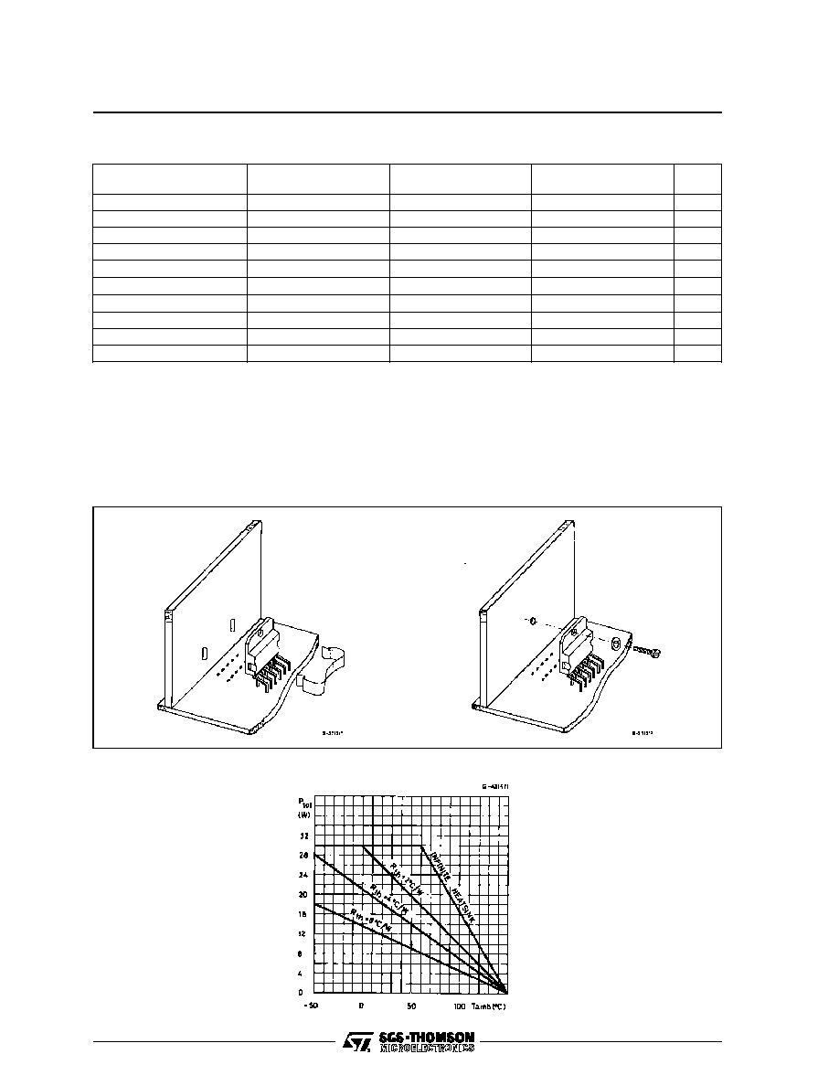
MOUNTING INSTRUCTIONS
The power dissipated in the circuit must be re-
moved by adding an external heatsink.
Thanks to the MULTIWATT
Æ
package attaching
the heatsink is very simple, a screw or a compres-
sion spring (clip) being sufficient. Between the
heatsink and the package it is better to insert a layer
of silicon grease, to optimize the thermal contact ;
no electrical isolation is needed between the two
surfaces.
2170-10.EPS
/
2170-11.EPS
Figure 2 : Application Circuit
2170-12.EPS
Figure 5 : Maximum Allowable Power Dissipation versus Ambient Temperature
TDA2170
6/7
F
G
G1
L
L1
L7
S
H1
L3
S1
L4
H2
Dia. 1
A
M
C
D
M1
E
B
L2
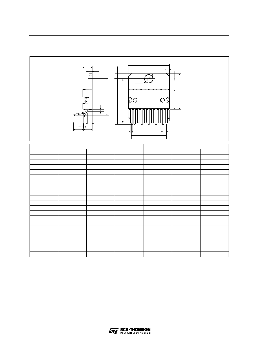
PMMUL11V.EPS
PACKAGE MECHANICAL DATA
11 PINS - PLASTIC MULTIWATT
Dimensions
Millimeters
Inches
Min.
Typ.
Max.
Min.
Typ.
Max.
A
5
0.197
B
2.65
0.104
C
1.6
0.063
E
0.49
0.55
0.019
0.022
F
0.88
0.95
0.035
0.037
G
1.57
1.7
1.83
0.062
0.067
0.072
G1
16.87
17
17.13
0.664
0.669
0.674
H1
19.6
0.772
H2
20.2
0.795
L
21.5
22.3
0.846
0.878
L1
21.4
22.2
0.843
0.874
L2
17.4
18.1
0.685
0.713
L3
17.25
17.5
17.75
0.679
0.689
0.699
L4
10.3
10.7
10.9
0.406
0.421
0.429
L7
2.65
2.9
0.104
0.114
M
4.1
4.3
4.5
0.161
0.169
0.177
M1
4.88
5.08
5.3
0.192
0.200
0.209
S
1.9
2.6
0.075
0.102
S1
1.9
2.6
0.075
0.102
Dia. 1
3.65
3.85
0.144
0.152
MUL11V.TBL
Information furnished is believed to be accurate and reliable. However, SGS-THOMSON Microelectronics assumes no responsibility
for the consequences of use of such information nor for any infringement of patents or other rights of third parties which may result
from its use. No licence is granted by implication or otherwise under any patent or patent rights of SGS-THOMSON Microelectronics.
Specifications mentioned in this publication are subject to change without not ice. This publication supersedes and replaces all
information previously supplied. SGS-THOMSON Microelectronics products are not authorized for use as critical components in life
support devices or systems without express written approval of SGS-THOMSON Microelectronics.
©
1994 SGS-THOMSON Microelectronics - All Rights Reserved
Purchase of I
2
C Components of SGS-THOMSON Microelectronics, conveys a license under the Philips
I
2
C Patent. Rights to use these components in a I
2
C system, is granted provided that the system conforms to
the I
2
C Standard Specifications as defined by Philips.
SGS-THOMSON Microelectronics GROUP OF COMPANIES
Australia - Brazil - China - France - Germany - Hong Kong - Italy - Japan - Korea - Malaysia - Malta - Morocco
The Netherlands - Singapore - Spain - Sweden - Switzerland - Taiwan - Thailand - United Kingdom - U.S.A.
TDA2170
7/7