 | –≠–ª–µ–∫—Ç—Ä–æ–Ω–Ω—ã–π –∫–æ–º–ø–æ–Ω–µ–Ω—Ç: TDA2320AN | –°–∫–∞—á–∞—Ç—å:  PDF PDF  ZIP ZIP |
.
WIDE SUPPLY VOLTAGE RANGE (3 to 36V)
.
SINGLE OR SPLIT SUPPLY OPERATION
.
VERY LOW CURRENT CONSUMPTION
(0.8mA)
.
VERY LOW DISTORTION
.
NO POP-NOISE
N
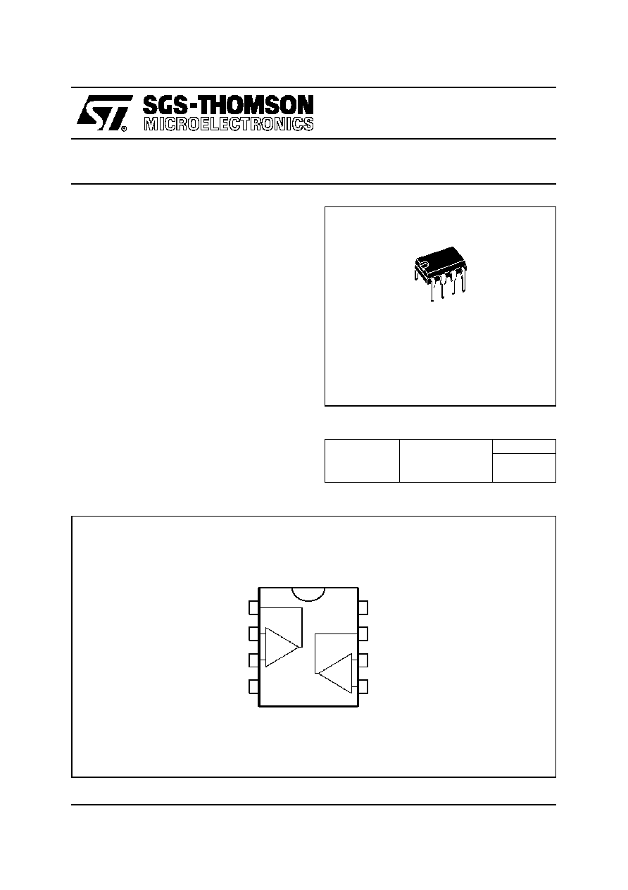
DIP8
(Plastic Package)
1
2
3
4
5
6
7
8
Inve rting Input 2
Output 2
Non-inverting Input 2
Output 1
Inverting Input 1
Non-inve rting Input 1
GND
CC
V
-
+
-
+
PIN CONNECTIONS (top view)
STEREO AMPLIFIER
TDA2320A
DESCRIPTION
The TDA2320A is a stereo class A preamplifier in-
tended for application in portable cassette players
and high quality audio systems.
The TDA2320A is a monolithic integrated circuit in
a 8 lead plastic dip.
October 1997
ORDER CODES
Part Number
Temperature
Range
Package
N
TDA2320A
-40
o
C, +105
o
C
∑
1/12

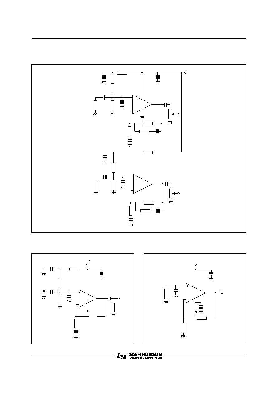
Inverting
Input
Non-inverting
Input
R1
R3
R5
R6
Q3
D3
D5
Q6
Q8
Q11
Q13
Q14
Q4
Q9
R7
R8
Q15
Q16
Q12
Q17
Q7
Q5
D4
Q10
R4
R2
C1
Output
Q2
Q1
D1
D2
C2
V
CC
GND
SCHEMATIC DIAGRAM (1/2 TDA2320A)
ABSOLUTE MAXIMUM RATINGS
Symbol
Parameter
Value
Unit
V
CC
Supply Voltage
36
V
P
tot
Total Power Dissipation at T
amb
= 70
o
C
400
mW
T
stg
, T
j
Storage and Junction Temperature
≠40 to 150
o
C
TDA2320A
2/12
ELECTRICAL CHARACTERISTICS
V
CC
= 15V, T
amb
= 25
o
C (unless otherwise specified) (refer to the test circuits)
Symbol
Parameter
Min.
Typ.
Max.
Unit
V
CC
Supply Voltage (*)
3
36
V
I
CC
Supply Current (*)
0.8
2
mA
I
ib
Input Bias Current
150
500
nA
V
io
Input Offset Voltage
R
s
10k
1
5
mV
I
io
Input Offset Current
10
50
nA
A
vd
Open Loop Voltage Gain
V
CC
= 15V
f = 333Hz
f = 1kHz
f = 10kHz
V
CC
= 4.5V
f = 1kHz
80
70
50
70
dB
V
OPP
Output Voltage Swing (f = 1kHz, R
L
= 600
) (*)
V
CC
= 15V
V
CC
= 4.5V
13
2.5
V
GBP
Gain-bandwidth Product
f = 20kHz
1.5
2.5
MHz
FBP
Power Bandwidth (*)
V
o
= 5V
PP
, THD = 1%
40
70
kHz
SR
Slew Rate (*)
1
1.6
V/
µ
s
THD
Distortion (V
o
= 2V, A
V
= 20dB) (*)
f = 1kHz
f = 10kHz
0.03
0.08
%
e
n
Equivalent Input Noise Voltage (**)
Curve A
R
s
= 50
R
s
= 600
R
s
= 5k
B = 22Hz to 22kHz
R
s
= 50
R
s
= 600
R
s
= 5k
f = 1kHz
R
s
= 600
1
1.1
1.5
1.3
1.5
2
9
1.4
µ
V
nV
Hz
V
O1
/V
02
Channel Separation (**)
f = 1kHz
100
dB
SVR
Supply Voltage Rejection Ratio(**)
f = 100Hz
80
dB
(*) Test circuit of figure 1
(**) Test circuit of figure 2
TDA2320A
3/12
1/2
TDA2320A
1/2
TDA2320A
22
µ
F
18k
82k
4.7
µ
F
0.3mV
TAPE
HEAD
150
220pF
15k
180k
22
µ
F
18k
10nF
20k
1
µ
F
7
8
5
6
4
100k
0.1
µ
F
22
µ
F
82k
4.7
µ
F
0.3mV
TAPE
HEAD
150
220pF
15k
180k
22
µ
F
10nF
20k
1
µ
F
1
3
2
100k
V
CC
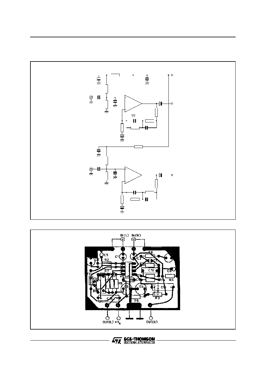
TYPICAL APPLICATION
STEREO PREAMPLIFIER FOR CASSETTE PLAYERS
1/2
TDA2320A
22
µ
F
18k
82k
150
220pF
22k
1
µ
F
100k
0.1
µ
F
V
CC
0.22
µ
F
IN
OUT
47
µ
F
Rx
TEST CIRCUITS
Figure 1
1/2
TDA2320A
33
220pF
0.1
µ
F
0.1
µ
F
OUT
+7.5V
3.3k
-7.5V
R
s
Figure 2
TDA2320A
4/12
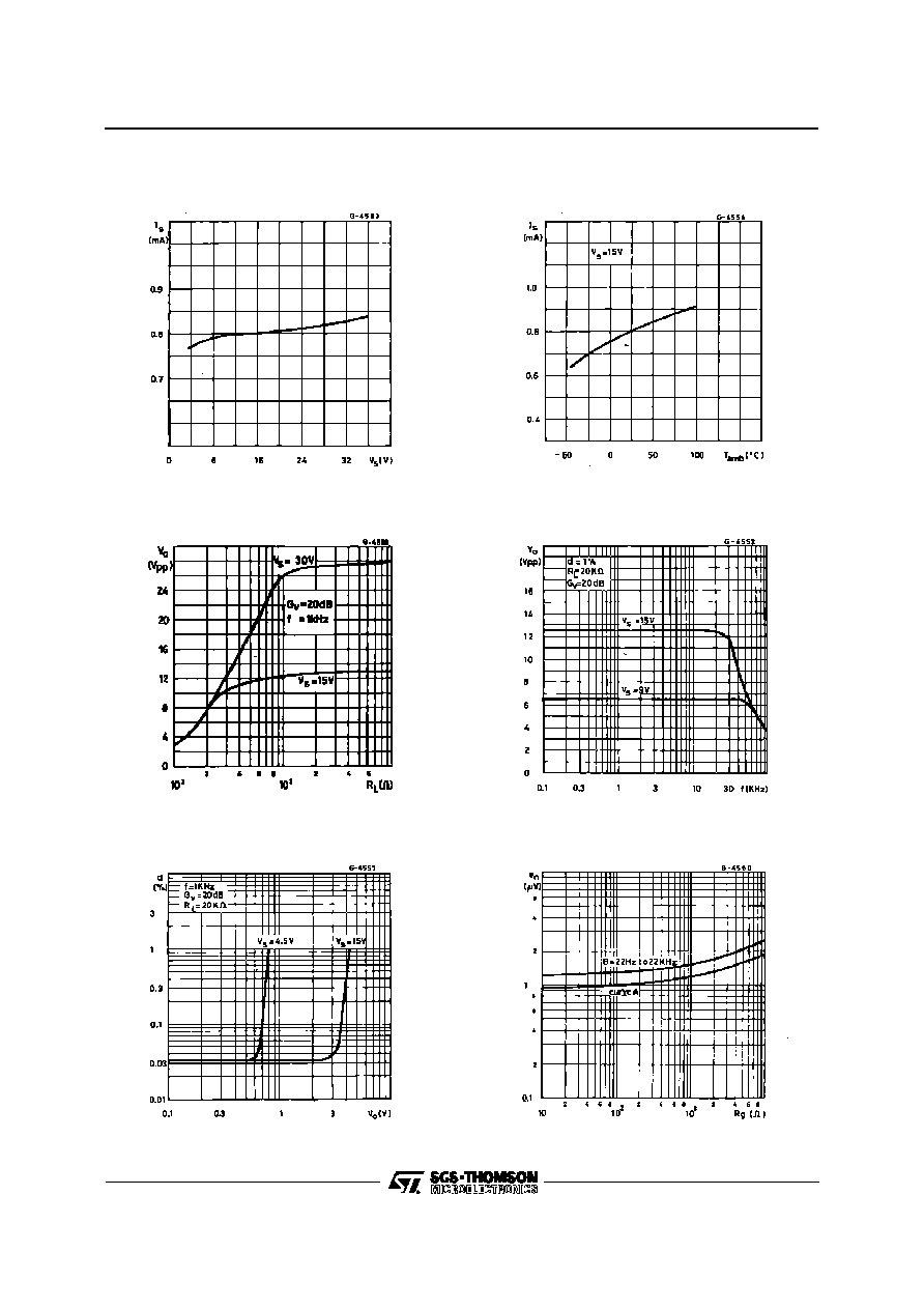
Figure 3 : Supply Current versus Supply
Voltage
Figure 4 : Supply Current versus Ambient
Temperature
Figure 5 : Output Voltage Swing versus
Load Resistance
Figure 6 : Power Ba ndwidth
Figure 7 : Total Harmonic Distortion
versusOutput Voltage
Figure 8 : Total Input Noise versus So urce
Resistance
TDA2320A
5/12

Figure 9 : Noise Density versus
Frequency
Figure 10 :RIAA Preamplifier Response
Figure 11 :Tape Preamplifier Frequency
TDA2320A
6/12
1/2
TDA2320A
22
µ
F
R5
18k
R1
100k
4.7
µ
F
R7
820
100pF
R10
22k
10
µ
F
R6
18k
15nF
1
µ
F
7
8
5
6
4
R2
120k
0.1
µ
F
C13
C3
C5
IN (L)
+15V
OUT (L)
C14
R13
1k
3.3nF
C9
R9
220k
C10
C7
1/2
TDA2320A
22
µ
F
R3
100k
4.7
µ
F
R8
820
100pF
R12
22k
10
µ
F
15nF
1
µ
F
1
3
2
R4
120k
C4
C6
IN (R)
OUT (R)
C15
R14
1k
3.3nF
C11
R11
220k
C12
C8
C1
C2
APPLICATION INFORMATION
Figure 12 : Stereo RIAA Preamplifier
Figure 13 : P.C. Board and Components layout of the Circuit of figure 12
TDA2320A
7/12
1/2
TDA2320A
0.22
µ
F
7
8
5
6
4
10k
10k
+15V
100nF
5.6nF
-15V
100nF
5.6k
5k
0.47
µ
F
TO
WOOFER
AMPLIFIER
1/2
TDA2320A
1
3
2
10k
5.6k
5k
0.1
µ
F
TO
TWEETER
AMPLIFIER
22k
5.6nF
5.6nF
IN
12nF
f = 2kHz
c
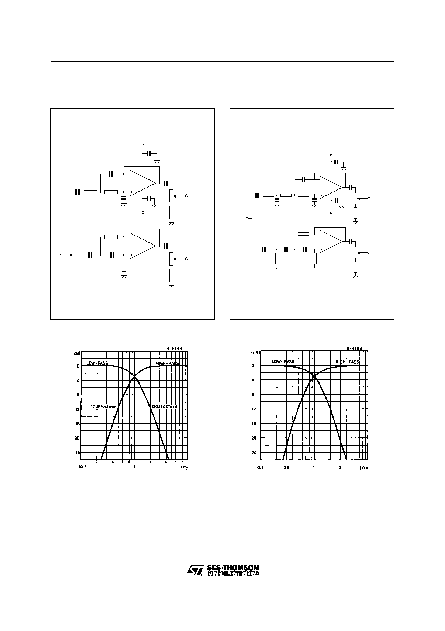
Figure 14 : Second Order 2kHz Butterworth
Crossover Filter for Hi-Fi Active
Boxes
Figure 16 : Frequency Response
(circuit of figure 14)
1/2
TDA2320A
C1
0. 22
µ
F
7
8
5
6
4
+15V
100nF
C4
1.2nF
-15V
100nF
R4
5.6k
5k
C5
0.47
µ
F
WOOFER
AMPLIFIER
1/2
TDA2320A
1
3
2
R6
8.2k
R8
5.6k
5k
C9
0.1
µ
F
TWEETER
AMPLIFIER
R7
47k
C6
4.7nF
INPUT
C3
6.8nF
f = 2.8kHz
c
R1
12k
R2
12k
C2
4.7nF
R3
12k
C7
4.7nF
R5
12k
C8
4.7nF
P1
P2
Figure 15 :Third Order 2.8kHz Bessel
Crossover Filter for Hi-Fi
Actives Boxes
Figure 17 : Frequency Response
(circuit of figure 15)
TDA2320A
8/12

0.3
µ
F
1/2
TDA2320A
1
3
2
10k
22k
IN
56nF
56nF
0.1
µ
F
1/2
TDA2320A
7
5
6
0.47
µ
F
5k
5.6k
1.8nF
12k
12k
12k
10nF
V
CC
V
CC
6.8nF
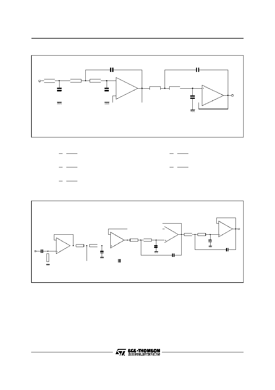
Figure 18 : 200Hz to 2kHz Active Bandpass Filter for Midrange Speakers
C
-
C
V
in
22k
10k
1/2
TDA2320A
3
2
1
V
out
Figure 19 : Subsonic Filter
f
c
(Hz)
C (
µ
F)
15
22
30
55
100
0.68
0.47
0.33
0.22
0.1
f
c
(kHz)
C1 (nF)
C2 (nF)
3
5
10
15
3.9
2.2
1.2
0.68
6.8
4.7
2.2
1.5
10k
C1
-
C2
V
in
V
out
10k
3
2
1/2
TDA2320A
1
Figure 20 :High-cut Filter
TDA2320A
9/12
R1
C1
-
R2
C2
C
R
R3
C3
-
R4
C4
1st order
2nd order
3rd order
i
i
1/2
TDA2320A
3
2
1
1/2
TDA2320A
5
6
7
Figure 21 : Fifth Order 3.4kHz Low-pass Butterworth Filter
C1
=
1.354 .
1
R
.
1
2
f
c
=
6.33nF
C1
=
0.421 .
1
R
.
1
2
f
c
=
1.97nF
C2
=
1.753 .
1
R
.
1
2
f
c
=
8.20nF
C3
=
0.309 .
1
R
.
1
2
f
c
=
1.45nF
C4
=
3.325 .
1
R
.
1
2
f
c
=
15.14nF
The attenuation of the filter is 30dB at 6.8kHz and
better than 60dB at 15kHz.
For f
c
= 3.4kHz and R
i
= R1 = R2 = R3 = R4 = 10k
, we obtain :
-
10k
3.54nF
10k
60nF
-
10k
16.3nF
10k
220nF
-
10k
86.1nF
10k
161nF
-
0.47
µ
F
56k
2
3
1
1/2
TDA
2320A
6
5
7
1/2
TDA
2320A
2
3
1
1/2
TDA
2320A
6
5
7
1/2
TDA
2320A
Figure 22 : Sixth-pole 355Hz Low-pass Filter (Chebychev type)
This is a 6-pole Chebychev type with
±
0.25dB ripple
in the passband.A decoupling stage is used to avoid
the influence of the input impedance of the filter's
characteristics.
The attenuation is about 55dB at 710Hz and
reaches 80dB at 1065Hz. The in band attenuation
is limited in practice to the
±
0.25dB ripple and does
not exceed 1/2dB at 0.9f
c
.
TDA2320A
10/12

1/2
TDA2320A
OUT
1/2
TDA2320A
IN
0.22
µ
F
3
2
1
+15V
100nF
56k
-15V
6
4
1.8k
500k
100k
100k
3.6k
11k
47nF
47nF
22nF
4.7nF
6
5
7
TREBLE
1.8k
11k
MIDRANGE
3.6k
BASS
11k
100nF
Figure 23 : Three Band Tone Control
Figure 24 :Frequency Response of the
Circuit of figure 23
A : all controls flat
B : bass & treble boost, mid flat
C : bass & treble cut, mid flat
D : mid boost, bass & treble flat
E : mid cut, bass treble flat
TDA2320A
11/12
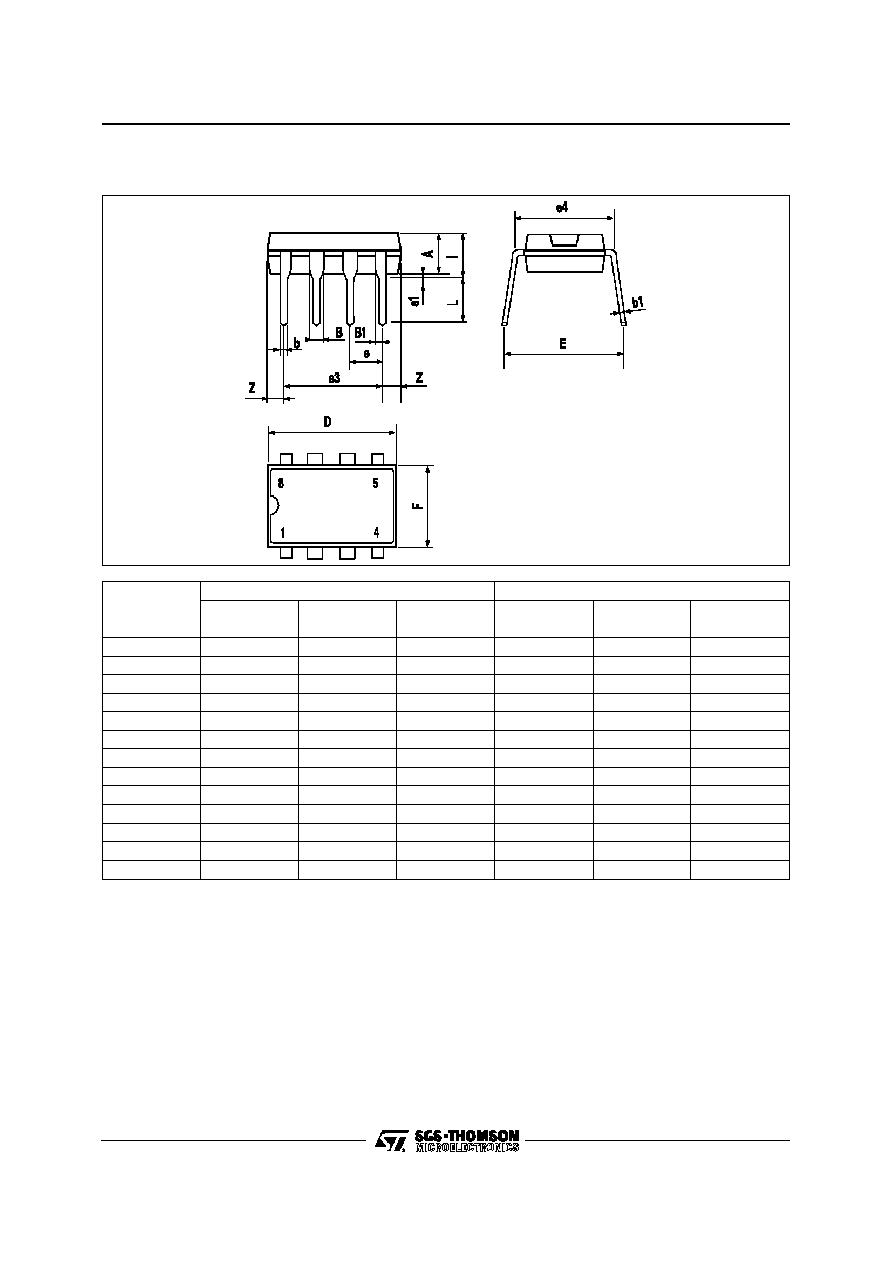
PM-DIP8.EPS
PACKAGE MECHANICAL DATA
8 PINS -PLASTIC DIP
Dimensions
Millimeters
Inches
Min.
Typ.
Max.
Min.
Typ.
Max.
A
3.32
0.131
a1
0.51
0.020
B
1.15
1.65
0.045
0.065
b
0.356
0.55
0.014
0.022
b1
0.204
0.304
0.008
0.012
D
10.92
0.430
E
7.95
9.75
0.313
0.384
e
2.54
0.100
e3
7.62
0.300
e4
7.62
0.300
F
6.6
0260
i
5.08
0.200
L
3.18
3.81
0.125
0.150
Z
1.52
0.060
DIP8.TBL
Information furnished is believed to be accurate and reliable. However, SGS-THOMSON Microelectronics assumes no responsi-
bility for the consequences of use of such information nor for any infringement of patents or other rights of third parties which
may result from its use. No license is granted by implication or otherwise under any patent or patent rights of SGS-THOMSON
Microelectronics. Specifications mentioned in this publ ication are subject to change without notice. This publication supersedes
and replaces all information previously supplied. SGS-THOMSON Microelectronics products are not authorized for use as critical
components in life support devices or systems without express written approval of SGS-THOMSON Microelectronics.
©
1997 SGS-THOMSON Microelectronics ≠ Printed in Italy ≠ All Rights Reserved
SGS-THOMSON Microelectronics GROUP OF COMPANIES
Australia - Brazil - Canada - China - France - Germany - Hong Kong - Italy - Japan - Korea - Malaysia - Malta - Morocco
The Netherlands - Singapore - Spain - Sweden - Switzerland - Taiwan - Thailand - United Kingdo m - U.S.A.
ORDER
CODE
:
TDA2320A
12/12