TDA2822
March 1995
DUAL POWER AMPLIFIER
.
SUPPLY VOLTAGE DOWN TO 3 V
.
LOW CROSSOVER DISTORSION
.
LOW QUIESCENT CURRENT
.
BRIDGE OR STEREO CONFIGURATION
DESCRIPTION
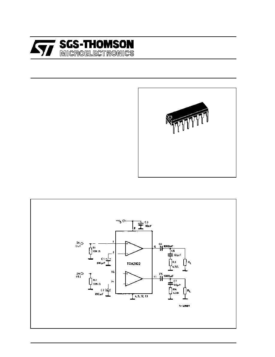
The TDA2822 is a monolithic integrated circuit in
12+2+2 powerdip, intended for use as dual audio
power amplifier in portable radios and TS sets.
POW ERDIP
(Plastic 12+2+2)
ORDERING NUMBER : TDA2822
TYPICAL APPLICATION CIRCUIT (STEREO)
1/11
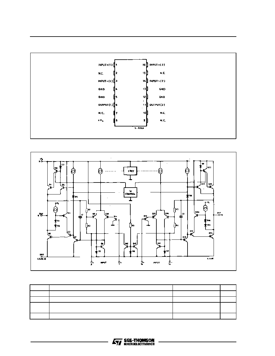
SCHEMATIC DIAGRAM
ABSOLUTE MAXIMUM RATINGS
Symbol
Parameter
Value
Unit
V
s
Supply Voltage
15
V
I
o
Output Peak Current
1.5
A
P
tot
Total Power Dissipation at T
amb
= 50
∞
C
at T
case
= 70
∞
C
1.25
4
W
W
T
stg
, T
j
Storage and Junction Temperature
≠ 40 to 150
∞
C
PIN CONNECTION (top view)
TDA2822
2/11

THERMAL DATA
Symbol
Parameter
Value
Unit
R
th j-amb
R
th j-case
Thermal Resistance Junction-ambient
Thermal Resistance Junction-pins
Max
Max
80
20
∞
C/W
∞
C/W
ELECTRICAL CHARACTERISTICS (Vs = 6 V, T
amb
= 25
∞
C, unless otherwise specified)
STEREO (test circuit of fig. 1)
Symbol
Parameter
Test Condition
Min.
Typ.
Max.
Unit
V
s
Supply Voltage
3
15
V
V
c
Quiescent Output Voltage
V
s
= 9 V
V
s
= 6 V
4
2.7
V
V
I
d
Quiescent Drain Current
6
12
mA
I
b
Input Bias Current
100
nA
P
o
Output Power
(each channel)
d = 10 %
f = 1 kHz
V
s
= 9 V
R
L
= 4
V
s
= 6 V
R
L
= 4
V
s
= 4.5 V R
L
= 4
1.3
0.45
1.7
0.65
0.32
W
W
W
G
v
Closed Loop Voltage Gain
f = 1 kHz
36
39
41
dB
R
i
Input Resistance
f = 1 kHz
100
k
e
N
Total Input Noise
R
s
= 10 k
B = 22 Hz to 22 kHz
Curve A
2.5
2
µ
V
µ
V
SVR
Supply Voltage Rejection
f = 100 Hz
24
30
dB
CS
Channel Separation
R
g
= 10 k
f = 1 kHz
50
dB
BRIDGE (test circuit of fig. 2)
V
s
Supply Voltage
3
15
V
I
d
Quiescent Drain Current
R
L
=
6
12
mA
V
os
Output Offset Voltage
R
L
= 8
10
60
mV
I
b
Input Bias Current
100
nA
P
o
Output Power
d = 10 %
f = 1 kHz
V
s
= 9 V
R
L
= 8
V
s
= 6 V
R
L
= 8
V
s
= 4.5 V R
L
= 4
2.7
0.9
3.2
1.35
1
W
W
W
d
Distortion (f = 1 kHz)
R
L
= 8
P
o
= 0.5 W
0.2
%
G
v
Closed Loop Voltage Gain
f = 1 kHz
39
dB
R
i
Input Resistance
f = 1 kHz
100
k
e
N
Total Input Noise
R
s
= 10 k
B = 22 Hz to 22 kHz
Curve A
3
2.5
µ
V
µ
V
SVR
Supply Voltage Rejection
f = 100 Hz
40
dB
TDA2822
3/11
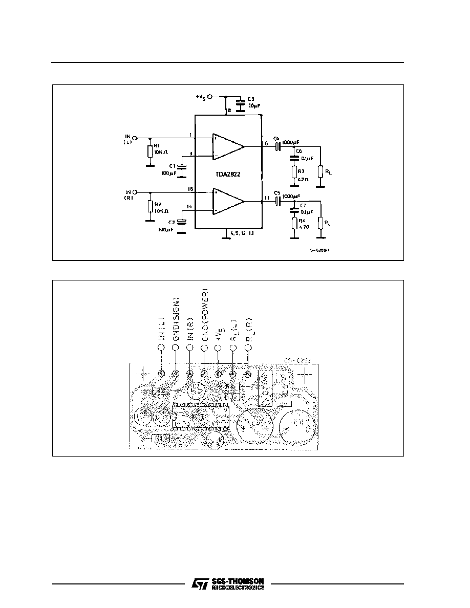
Figure 1 : Test Circuit (stereo).
Figure 2 : P.C. Board and Components Layout of the Circuit of Figure 1 (1:1 scale).
TDA2822
4/11

Figure 3 : Test Circuit (bridge).
Figure 4 : P.C. Board and Components Layout of the Circuit of Figure 3 (1:1 scale).
TDA2822
5/11