 | –≠–ª–µ–∫—Ç—Ä–æ–Ω–Ω—ã–π –∫–æ–º–ø–æ–Ω–µ–Ω—Ç: TDA7233 | –°–∫–∞—á–∞—Ç—å:  PDF PDF  ZIP ZIP |
TDA7233
TDA7233D
1W AUDIO AMPLIFIER WITH MUTE
OPERATING VOLTAGE 1.8 TO 15V
EXTERNAL MUTE OR POWER DOWN
FUNCTION
IMPROVED SUPPLY VOLTAGE REJECTION
LOW QUIESCENT CURRENT
HIGH POWER CAPABILITY
LOW CROSSOVER DISTORTION
DESCRIPTION
The TDA7233/D is a monolithic integrated circuit
in 8 pin Minidip or SO8 package, intended for use
as class AB power amplifier with a wide range of
supply voltage from 1.8V to 15V in portable play-
ers, cordless telephones and Cellular Radios.
This is advanced information on a new product now in development or undergoing evaluation. Details are subject to change without notice.
September 2003
Æ
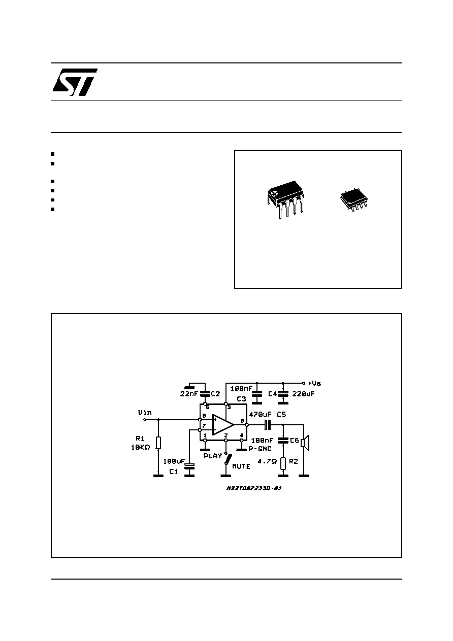
TEST AND APPLICATION CIRCUIT
Note: Switch Open = Mute
Switch Closed = Play
Minidip SO8
ORDERING NUMBERS:
TDA7233 TDA7233D
1/7

ABSOLUTE MAXIMUM RATINGS
Symbol
Parameter
Value
Unit
V
S
Supply Voltage
16
V
I
O
Output Peak Current
1
A
P
tot
Total Power Dissipation at T
amb
= 50
∞
C
1
W
T
stg
, T
j
Storage and Junction Temperature
≠40 to 150
∞
C
THERMAL DATA
Symbol
Parameter
SO8
Minidip
Unit
R
th j-amb
Thermal Resistance Junction-ambient Max.
200
100
∞
C/W
PIN CONNECTIONS (Top views)
Minidip
SO8
TDA7233 - TDA7233D
2/7
ELECTRICAL CHARACTERISTICS (V
s
= 6 V, T
amb
= 25
∞
C, unless otherwise specified)
Symbol
Parameter
Test Condition
Min.
Typ.
Max.
Unit
V
s
Supply Voltage
1.8
15
V
V
o
Quiescent Out Voltage
2.7
V
V
s
= 3 V
V
s
= 9 V
1.2
4.2
V
V
I
d
Quiescent Drain Current
MUTE HIGH
3.6
9
mA
MUTE LOW
0.4
I
b
Input Bias Current
100
nA
P
o
Output Power
d = 10 % f = 1 KHz
V
s
= 12 V R
L
= 8
V
s
= 9 V R
L
= 4
V
s
= 9 V R
L
= 8
V
s
= 6 V R
L
= 8
V
s
= 6 V R
L
= 4
V
s
= 3 V R
L
= 4
V
s
= 3 V R
L
= 8
1.9
1.6
1
0.4
0.7
110
70
W
W
W
W
W
mW
mW
d
Distortion
P
o
= 0.5 W
f = 1 kHz
R
L
= 8
V
s
= 9 V
0.3
%
G
v
Closed Loop Voltage Gain
f = 1 kHz
39
dB
R
IN
Input Resistance
f = 1 kHz
100
K
e
N
Total Input Noise
(R
s
= 10 k
)
B = Curve A
2
µ
V
B = 22 Hz to 22 kHz
3
SVR
Supply Voltage Rejection
f = 100 Hz, R
g
= 10 K
45
dB
MUTE Attenuation
V
o
= 1 V f = 100 Hz to 10 kHz
70
dB
MUTE Threshold
0.6
V
I
M
MUTE Current
V
S
= 15V
0.4
mA
TDA7233 - TDA7233D
3/7

Figure 1: Output Power vs. Supply Voltage
Figure 2: Supply Voltage Rejection vs. Frequency
Figure 3: DC Output Voltage vs. Supply Voltage
Figure 4: Quiescent Current vs. Supply Voltage
Figure 5: Total Dissipated Power vs. Supply
Voltage
TDA7233 - TDA7233D
4/7
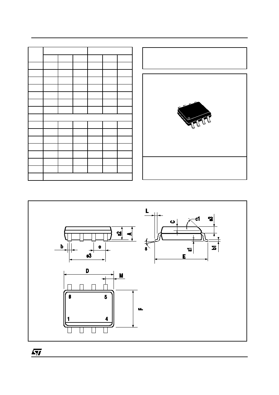
DIM.
mm
inch
MIN.
TYP.
MAX.
MIN.
TYP.
MAX.
A
1.75
0.069
a1
0.1
0.25
0.004
0.010
a2
1.65
0.065
a3
0.65
0.85
0.026
0.033
b
0.35
0.48
0.014
0.019
b1
0.19
0.25
0.007
0.010
C
0.25
0.5
0.010
0.020
c1
45
∞
(typ.)
D (1)
4.8
5.0
0.189
0.197
E
5.8
6.2
0.228
0.244
e
1.27
0.050
e3
3.81
0.150
F (1)
3.8
4.0
0.15
0.157
L
0.4
1.27
0.016
0.050
M
0.6
0.024
S
8
∞
(max.)
(1) D and F do not include mold flash or protrusions. Mold flash or
potrusions shall not exceed 0.15mm (.006inch).
SO8
OUTLINE AND
MECHANICAL DATA
TDA7233 - TDA7233D
5/7