 | –≠–ª–µ–∫—Ç—Ä–æ–Ω–Ω—ã–π –∫–æ–º–ø–æ–Ω–µ–Ω—Ç: TDA7241BH | –°–∫–∞—á–∞—Ç—å:  PDF PDF  ZIP ZIP |

TDA7241B
20W BRIDGE AMPLIFIER FOR CAR RADIO
VERY LOW STAND-BY CURRENT
GAIN = 32dB
OUTPUT PROTECTED AGAINST SHORT
CIRCUITS
TO
GROUND
AND ACROSS
LOAD
COMPACT HEPTAWATT PACKAGE
DUMP TRANSIENT
THERMAL SHUTDOWN
LOUDSPEAKER PROTECTION
HIGH CURRENT CAPABILITY
LOW DISTORTION / LOW NOISE
DESCRIPTION
The TDA7241B is a 20W bridge audio amplifier
IC designed specially for car radio applications.
Thanks to the low external part count and com-
pact
Heptawatt
7-pin
power
package
the
TDA7241B occupies little space on the printed
circuit board.
Reliable operation is guaranteed by a compre-
hensive array of on-chip protection features.
These include protection against AC and DC out-
put short circuits (to ground and across the load),
load dump transients, and junction overtempera-
ture. Additionally, the TDA7241B protects the
loudspeaker when one output is short-circuited to
ground.
July 1997
Heptawatt
ORDERING NUMBER: TDA7241BH
Figure 1: Test and Appliication Circuit
1/7

ABSOLUTE MAXIMUM RATINGS
Symbol
Parameter
Value
Unit
V
S
Operating Supply Voltage
18
V
V
S
DC Supply Voltage
28
V
V
S
Peak Supply Voltage (t = 50ms)
40
V
I
O
Peak Output Current (non repetitive t = 0.1ms)
4.5
A
I
O
Peak Output Current (repetitive f > 10Hz)
3.5
A
P
tot
Power Dissipation at T
case
= 85
∞
C
16
W
T
stg
, T
j
Storage and Junction Temperature
-40 to 150
∞
C
THERMAL DATA
Symbol
Description
Value
Unit
R
th j-case
Thermal Resistance Junction-case
Max
4
∞
C/W
PIN CONNECTION (Top view)
TDA7241B
2/7

ELECTRICAL CHARACTERISTICS (Refer to the circuit of Fig. 1; V
S
= 14.4V; R
th
(heatsink) = 4
∞
C/W,
T
amb
= 25
∞
C, unless otherwise specified
Symbol
Parameter
Test Condition
Min.
Typ.
Max.
Unit
V
S
Supply Range
18
V
I
d
Total Quiescent Current
R
L
= 4
80
mA
V
OS
Output Offset Voltage
100
mV
P
O
Output Power
.
R
L
= 2
f = 1KHz d = 10%
R
L
= 4
.
R
L
= 8
18
26
20
12
W
d
Distortion
R
L
= 4
f = 1KHz
P
O
= 50mW to 12W
0.1
0.5
%
R
L
= 8
f = 1KHz
P
O
= 50mW to 6W
0.05
%
G
V
Voltage Gain
f = 1KHz
31
32
33
dB
SVR
Supply Voltage Rejection
f =100Hz R
g
= 10K
40
50
dB
E
n
Total Input Noise
B = Curve A
R
g
= 10K
2
µ
V
B = 22Hz to 22KHz R
S
= 10K
3
10
mV
Efficiency
R
L
= 4
f = 1KHz
P
O
= 20W
65
%
I
sb
Stand-by Current
100
µ
A
R
i
Input Resistance
f = 1KHz
70
K
V
i
Input Sensitivity
f = 1KHz
P
O
= 2W
R
L
= 4
70
mV
f
L
Low Frequency Roll Off (-3dB)
P
O
= 15W
R
L
= 4
30
Hz
f
H
High Frequency Roll Off (-3dB)
PO = 15W
R
L
= 4
25
KHz
A
S
Stand-by Attenuation
V
O
= 2Vrms
70
90
dB
V
TH
(pin.2)
Stand-by Threshold
1
V
T
sd
Thermal Shutdown Junction Temp.
150
∞
C
(*) B = Curve
(**) B = 22Hz to 22KHz
Figure 2: P.C. Board and Component Layout of the Circuit of Fig. 1 (1:1 scale).
TDA7241B
3/7
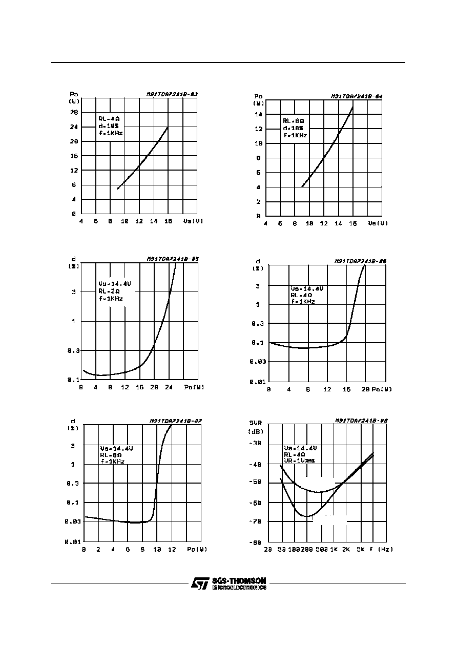
Figure 3: Output Power vs. Supply Voltage
Figure 4: Output Power vs. Supply Voltage
Figure 5: Distortion vs. Output Power
Figure 6: Distortion vs. Output Power
Figure 7: Distortion vs. Output Power
Figure 8: SVR vs. Frequency
R
g
= 10k
R
g
= 0
TDA7241B
4/7

Figure 9: Power Dissipation and Efficiency vs.
Output Power
Figure 10: Power Dissipation and Efficiency vs.
Output Power
TDA7241B
5/7