 | –≠–ª–µ–∫—Ç—Ä–æ–Ω–Ω—ã–π –∫–æ–º–ø–æ–Ω–µ–Ω—Ç: TDA7313N | –°–∫–∞—á–∞—Ç—å:  PDF PDF  ZIP ZIP |

TDA7313N
DIGITAL CONTROLLED STEREO AUDIO PROCESSOR
WITH LOUDNESS
INPUT MULTIPLEXER:
- 3 STEREO INPUTS
- SELECTABLE INPUT GAIN FOR OPTIMAL
ADAPTION TO DIFFERENT SOURCES
LOUDNESS FUNCTION
VOLUME CONTROL IN 1.25dB STEPS
TREBLE AND BASS CONTROL
FOUR SPEAKER ATTENUATORS:
- 4 INDEPENDENT SPEAKERS CONTROL
IN 1.25dB STEPS FOR BALANCE AND
FADER FACILITIES
- INDEPENDENT MUTE FUNCTION
ALL FUNCTIONS PROGRAMMABLE VIA SE-
RIAL I
2
C BUS
DESCRIPTION
The TDA7313N is a volume, tone (bass and treble)
balance (Left/Right) and fader (front/rear) processor
for quality audio applications in car radio and Hi-Fi
systems.
Selectable input gain and external loudness function
are provided. Control is accomplished by serial
I
2
C busmicroprocessor interface.
The AC signal setting is obtained by resistor networks
andswitches combined with operationalamplifiers.
Thanks to the used BIPOLAR/CMOS Tecnology,
Low Distortion, Low Noise and Low DC stepping are
obtained.
November 1999
Æ
DIP28
SO28
ORDERING NUMBERS:
TDA7313N
TDA7313ND
PIN CONNECTION (Top view)
1/14

THERMAL DATA
Symbol
Description
SO28
DIP28
Unit
R
th j-pins
Thermal Resistance Junction-pins
max
85
65
∞
C/W
QUICK REFERENCE DATA
Symbol
Parameter
Min.
Typ.
Max.
Unit
V
S
Supply Voltage
6
9
10
V
V
CL
Max. input signal handling
2
Vrms
THD
Total Harmonic Distortion V = 1Vrms f = 1KHz
0.01
0.1
%
S/N
Signal to Noise Ratio
106
dB
S
C
Channel Separation f = 1KHz
103
dB
Volume Control
1.25dB step
-78.75
0
dB
Bass and Treble Control
2db step
-14
+14
dB
Fader and Balance Control
1.25dB step
-38.75
0
dB
Input Gain
3.75dB step
0
11.25
dB
Mute Attenuation
100
dB
ABSOLUTE MAXIMUM RATINGS
Symbol
Parameter
Value
Unit
V
S
Operating Supply Voltage
10.2
V
T
amb
Operating Ambient Temperature
-40 to 85
∞
C
T
stg
Storage Temperature Range
-55 to +150
∞
C
TEST CIRCUIT
TDA7313N
2/14

L1
15
L1
L2
14
L2
L3
13
L3
INPUT
SELECTOR
+
GAIN
C1
C2
C3
LEFT
INPUTS
3x
2.2
µ
F
SUPPLY
R3
9
R3
R2
10
R2
R1
11
R1
C4
C5
C6
3x
2.2
µ
F
RIGHT
INPUTS
231
V
S
AGND
CREF
C9
2.2
µ
F
OUT(L)
IN(L)
17
16
VOL
+
LOUD
LOUD(L)
12
100nF
C14
BASS
19
5.6K
R2
BOUT(L)
18
BIN(L)
100nF
C15
RB
TREBLE
C17
2.7nF
TREBLE(L)
4
MUTE
D98AU888
SERIAL
BUS
DECODER
+
LATCHES
SPKR
ATT
25
VOL
+
LOUD
BASS
TREBLE
OUT(R)
IN(R)
C8
2.2
µ
F
76
100nF
C12
100nF
C13
5.6K
R1
BOUT(R)
BIN(R)
21
20
RB
2.7nF
C16
TREBLE(R)
MUTE
SPKR
ATT
28
27
26
22
SCL
SDA
DIGGND
BUS
OUT
RIGHT
REAR
OUT
LEFT
FRONT
5
22
µ
F
C7
8
LOUD(R)
C11
100nF
100nF
C10
MUTE
SPKR
ATT
OUT
LEFT
REAR
23
MUTE
SPKR
ATT
OUT
RIGHT
FRONT
24
BLOCK DIAGRAM
TDA7313N
3/14

ELECTRICAL CHARACTERISTICS (refer to the test circuit T
amb
= 25
∞
C, V
S
= 9V, R
L
= 10K
,
R
G
= 600
, all controls flat (G = 0), f = 1KHz unless otherwise specified)
Symbol
Parameter
Test Condition
Min.
Typ.
Max.
Unit
SUPPLY
V
S
Supply Voltage
6
9
10
V
I
S
Supply Current
8
11
mA
SVR
Ripple Rejection
60
80
dB
INPUT SELECTORS
R
II
Input Resistance
Input 1, 2, 3
35
50
70
K
V
CL
Clipping Level
2
2.5
Vrms
S
IN
Input Separation (2)
80
100
dB
R
L
Output Load resistance
pin 7, 17
2
K
G
INmin
Min. Input Gain
-1
0
1
dB
G
INmax
Max. Input Gain
11.25
dB
G
STEP
Step Resolution
3.75
dB
e
IN
Input Noise
G = 11.25dB
2
µ
V
V
DC
DC Steps
adjacent gain steps
4
20
mV
G = 18.75 to Mute
4
mV
VOLUME CONTROL
R
IV
Input Resistance
20
33
50
k
C
RANGE
Control Range
70
75
80
dB
A
VMIN
Min. Attenuation
-1
0
1
dB
A
VMAX
Max. Attenuation
70
75
80
dB
A
STEP
Step Resolution
0.5
1.25
1.75
dB
E
A
Attenuation Set Error
Av = 0 to -20dB
Av = -20 to -60dB
-1.25
-3
0
1.25
2
dB
dB
E
T
Tracking Error
2
dB
V
DC
DC Steps
adjacent attenuation steps
From 0dB to Av max
0
0.5
3
7.5
mV
mV
SPEAKER ATTENUATORS
C
range
Control Range
35
37.5
40
dB
S
STEP
Step Resolution
0.5
1.25
1.75
dB
E
A
Attenuation set error
1.5
dB
A
MUTE
Output Mute Attenuation
80
100
dB
V
DC
DC Steps
adjacent att. steps
from 0 to mute
0
1
3
10
mV
mV
BASS CONTROL (1)
Gb
Control Range
Max. Boost/cut
+12
+14
+16
dB
B
STEP
Step Resolution
1
2
3
dB
R
B
Internal Feedback Resistance
34
44
58
K
TREBLE CONTROL (1)
Gt
Control Range
Max. Boost/cut
+13
+14
+15
dB
T
STEP
Step Resolution
1
2
3
dB
TDA7313N
4/14

ELECTRICAL CHARACTERISTICS (continued)
Symbol
Parameter
Test Condition
Min.
Typ.
Max.
Unit
AUDIO OUTPUTS
V
OCL
Clipping Level
d = 0.3%
2
2.5
Vrms
R
L
Output Load Resistance
2
K
C
L
Output Load Capacitance
10
nF
R
OUT
Output resistance
30
75
120
V
OUT
DC Voltage Level
4.2
4.5
4.8
V
GENERAL
e
NO
Output Noise
BW = 20-20KHz, flat
output muted
all gains = 0dB
2.5
5
15
µ
V
µ
V
A curve all gains = 0dB
3
µ
V
S/N
Signal to Noise Ratio
all gains = 0dB; V
O
= 1Vrms
106
dB
d
Distortion
A
V
= 0, V
IN
= 1Vrms
A
V
= -20dB V
IN
= 1Vrms
V
IN
= 0.3Vrms
0.01
0.09
0.04
0.1
0.3
%
%
%
Sc
Channel Separation left/right
80
103
dB
Total Tracking error
A
V
= 0 to -20dB
-20 to -60 dB
0
0
1
2
dB
dB
BUS INPUTS
V
IL
Input Low Voltage
1
V
V
IH
Input High Voltage
3
V
I
IN
Input Current
-5
+5
µ
A
V
O
Output Voltage SDA
Acknowledge
I
O
= 1.6mA
0.4
V
Notes:
(1) Bass and Treble response see attached diagram (fig.16). The center frequency and quality of the resonance behaviour can be choosen by
the external circuitry. A standard first order bass response can be realized by a standard feedback network
(2) The selected input is grounded thru the 2.2
µ
F capacitor.
Figure 2: Loudnessvs. Frequency (C
LOUD
=
100nF) vs. Volume Attenuation
Figure 1: Loudness vs. Volume Attenuation
TDA7313N
5/14
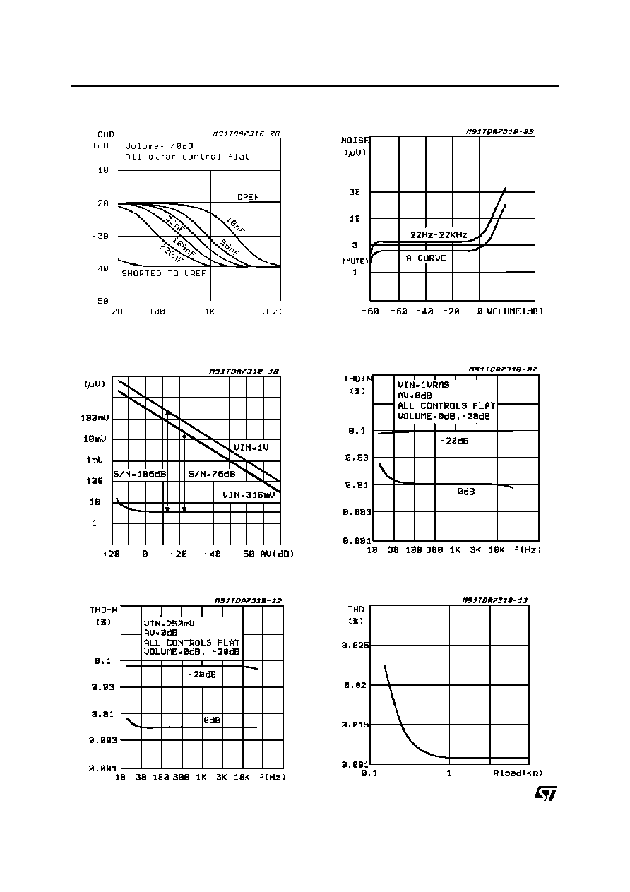
Figure 6: Distortion & Noise vs. Frequency
Figure 7: Distortion & Noise vs. Frequency
Figure 8: Distortion vs. Load Resistance
Figure 4: Noise vs. Volume/Gain Settings
Figure 5: Signal to Noise Ratio vs. Volume
Setting
Figure 3: Loudness vs. External Capacitors
TDA7313N
6/14

Figure 12: Output Clipping Level vs. Supply
Voltage
Figure 14: Supply Current vs. Temperature
Figure 13: Quiescent Current vs. Supply Voltage
Figure 10: Input Separation (L1
L2, L3, L4) vs.
Frequency
Figure 9: Channel Separation (L
R) vs.
Frequency
Figure 11: Supply Voltage Rejection vs.
Frequency
TDA7313N
7/14

I
2
C BUS INTERFACE
Data transmission from microprocessor to the
TDA7313N and viceversa takes place thru the 2
wires I
2
C BUS interface, consisting of the two
lines SDA and SCL (pull-up resistors to positive
supply voltage must be connected).
Data Validity
As shown in fig. 17, the data on the SDA line
must be stable during the high period of the clock.
The HIGH and LOW state of the data line can
only change when the clock signal on the SCL
line is LOW.
Start and Stop Conditions
As shown in fig.18 a start condition is a HIGH to
LOW transition of the SDA line while SCL is
HIGH. The stop condition is a LOW to HIGH tran-
sition of the SDA line while SCL is HIGH.
Byte Format
Every byte transferred on the SDA line must con-
tain 8 bits. Each byte must be followed by an ac-
knowledge bit. The MSB is transferred first.
Acknowledge
The master (
µ
P) puts a resistive HIGH level on the
SDA line during the acknowledge clock pulse (see
fig. 19). The peripheral (audioprocessor) that ac-
knowledges has to pull-down (LOW) the SDA line
during the acknowledge clock pulse, so that the
SDA line is stable LOW during this clock pulse.
The audioprocessor which has been addressed
has to generate an acknowledge after the recep-
tion of each byte, otherwise the SDA line remains
at the HIGH level during the ninth clock pulse
time. In this case the master transmitter can gen-
erate the STOP information in order to abort the
transfer.
Transmission without Acknowledge
Avoiding to detect the acknowledge of the audio-
processor, the
µ
P can use a simplier transmis-
sion: simply it waits one clock without checking
the slave acknowledging, and sends the new
data.
This approach of course is less protected from
misworking and decreases the noise immunity.
Figure 17: Data Validity on the I
2
CBUS
Figure 16: Typical Tone Response (with the ext.
components indicated in the test
circuit)
Figure 15: Bass Resistance vs. Temperature
TDA7313N
8/14

SOFTWARE SPECIFICATION
Interface Protocol
The interface protocol comprises:
A start condition (s)
A chip address byte, containing the TDA7313N
address (the 8th bit of the byte must be 0). The
TDA7313N must always acknowledge at the
end of each transmitted byte.
A sequence of data (N-bytes + acknowledge)
A stop condition (P)
TDA7313N ADDRESS
MSB
first byte
LSB
MSB
LSB
MSB
LSB
S
1
0
0
0
1
0
0
0
ACK
DATA
ACK
DATA
ACK
P
Data Transferred (N-bytes + Acknowledge)
ACK = Acknowledge
S = Start
P = Stop
MAX CLOCK SPEED 100kbits/s
SOFTWARE SPECIFICATION
Chip address
1
MSB
0
0
0
1
0
0
0
LSB
DATA BYTES
MSB
LSB
FUNCTION
0
1
1
1
1
0
0
0
0
1
1
0
0
1
1
1
B2
0
1
0
1
0
1
1
B1
B1
B1
B1
B1
G1
0
1
B0
B0
B0
B0
B0
G0
C3
C3
A2
A2
A2
A2
A2
S2
C2
C2
A1
A1
A1
A1
A1
S1
C1
C1
A0
A0
A0
A0
A0
S0
C0
C0
Volume control
Speaker ATT LR
Speaker ATT RR
Speaker ATT LF
Speaker ATT RF
Audio switch
Bass control
Treble control
Ax = 1.25dB steps; Bx = 10dB steps; Cx = 2dB steps; Gx = 3.75dB steps
Figure 18: Timing Diagram of I
2
CBUS
Figure 19: Acknowledge on the I
2
CBUS
TDA7313N
9/14

SOFTWARE SPECIFICATION (continued)
DATA BYTES (detailed description)
Volume
MSB
LSB
FUNCTION
0
0
B2
B1
B0
A2
A1
A0
Volume 1.25dB steps
0
0
0
0
1
1
1
1
0
0
1
1
0
0
1
1
0
1
0
1
0
1
0
1
0
-1.25
-2.5
-3.75
-5
-6.25
-7.5
-8.75
0
0
B2
B1
B0
A2
A1
A0
Volume 10dB steps
0
0
0
0
1
1
1
1
0
0
1
1
0
0
1
1
0
1
0
1
0
1
0
1
0
-10
-20
-30
-40
-50
-60
-70
For example a volume of -45dB is given by:
0 0 1 0 0 1 0 0
Speaker Attenuators
MSB
LSB
FUNCTION
1
1
1
1
0
0
1
1
0
1
0
1
B1
B1
B1
B1
B0
B0
B0
B0
A2
A2
A2
A2
A1
A1
A1
A1
A0
A0
A0
A0
Speaker LF
Speaker RF
Speaker LR
Speaker RR
0
0
0
0
1
1
1
1
0
0
1
1
0
0
1
1
0
1
0
1
0
1
0
1
0
-1.25
-2.5
-3.75
-5
-6.25
-7.5
-8.75
0
0
1
1
0
1
0
1
0
-10
-20
-30
1
1
1
1
1
Mute
For example attenuation of 25dB on speaker RF is given by:
1 0 1 1 0 1 0 0
TDA7313N
10/14
Audio Switch
MSB
LSB
FUNCTION
0
1
0
G1
G0
S2
S1
S0
Audio Switch
0
1
0
0
1
1
0
1
0
1
Stereo 1
Stereo 2
Stereo 3
Stereo 4 (*)
LOUDNESS ON
LOUDNESS OFF
0
0
1
1
0
1
0
1
+11.25dB
+7.5dB
+3.75dB
0dB
For example to select the stereo 2 input with a gain of +7.5dB LOUDNESS ON the 8bit string is:
0 1 0 0 1 0 0 1
(*) Stereo 4 is connected internally, but not available on pins.
Bass and Treble
0
0
1
1
1
1
0
1
C3
C3
C2
C2
C1
C1
C0
C0
Bass
Treble
0
0
0
0
0
0
0
0
1
1
1
1
1
1
1
1
0
0
0
0
1
1
1
1
1
1
1
1
0
0
0
0
0
0
1
1
0
0
1
1
1
1
0
0
1
1
0
0
0
1
0
1
0
1
0
1
1
0
1
0
1
0
1
0
-14
-12
-10
-8
-6
-4
-2
0
0
2
4
6
8
10
12
14
C3 = Sign
For example Bass at -10dB is obtained by the following 8 bit string:
0 1 1 0 0 0 1 0
TDA7313N
11/14

SO28
DIM.
mm
inch
MIN.
TYP.
MAX.
MIN.
TYP.
MAX.
A
2.65
0.104
a1
0.1
0.3
0.004
0.012
b
0.35
0.49
0.014
0.019
b1
0.23
0.32
0.009
0.013
C
0.5
0.020
c1
45
∞
(typ.)
D
17.7
18.1
0.697
0.713
E
10
10.65
0.394
0.419
e
1.27
0.050
e3
16.51
0.65
F
7.4
7.6
0.291
0.299
L
0.4
1.27
0.016
0.050
S
8
∞
(max.)
OUTLINE AND
MECHANICAL DATA
TDA7313N
12/14

DIM.
mm
inch
MIN.
TYP.
MAX.
MIN.
TYP.
MAX.
a1
0.63
0.025
b
0.45
0.018
b1
0.23
0.31
0.009
0.012
b2
1.27
0.050
D
37.34
1.470
E
15.2
16.68
0.598
0.657
e
2.54
0.100
e3
33.02
1.300
F
14.1
0.555
I
4.445
0.175
L
3.3
0.130
DIP28
OUTLINE AND
MECHANICAL DATA
TDA7313N
13/14

Information furnished is believed to be accurate and reliable. However, STMicroelectronics assumes no responsibility for the consequences
of use of such information nor for any infringement of patents or other rights of third parti es which may result from its use. No license is
granted by implication or otherwise under any patent or patent rights of STMicroelectronics. Specification mentioned in this publication are
subject to change without notice. This publication supersedes and replaces all information previously supplied. STMicroelectronics products
are not authorized for use as critical components in life support devices or systems without express written approval of STMicroelectronics.
The ST logo is a registered trademark of STMicroelectronics
©
1999 STMicroelectronics ≠ Printed in Italy ≠ All Rights Reserved
STMicroelectronics GROUP OF COMPANIES
Australia - Brazil - China - Finland - France - Germany - Hong Kong - India - Italy - Japan - Malaysia - Malta - Morocco -
Singapore - Spain - Sweden - Switzerland - United Kingdom - U.S.A.
http://www.st.com
Purchase of I
2
C Components of STMicroelectronics, conveys a license under the Philips I
2
C Patent
Rights to use these components in an I
2
C system, provided that the system conforms to the I
2
C
Standard Specifications as defined by Philips.
TDA7313N
14/14