 | –≠–ª–µ–∫—Ç—Ä–æ–Ω–Ω—ã–π –∫–æ–º–ø–æ–Ω–µ–Ω—Ç: TDA7437 | –°–∫–∞—á–∞—Ç—å:  PDF PDF  ZIP ZIP |

TDA7437
DIGITALLY CONTROLLED AUDIO PROCESSOR
INPUT MULTIPLEXER
- FOUR STEREO, ONE MONO INPUT, AND
ONE DIFFERENTIAL INPUT
- SELECTABLE INPUT GAIN FOR OPTIMAL
ADAPTATION TO DIFFERENT SOURCES
FULLY
PROGRAMMABLE
LOUDNESS
FUNCTION
VOLUME CONTROL IN 1dB STEPS INCLUD-
ING GAIN UP TO 16dB
ZERO CROSSING MUTE, SOFT MUTE AND
DIRECT MUTE
BASS AND TREBLE CONTROL
FOUR SPEAKER ATTENUATORS
- FOUR INDEPENDENT SPEAKERS
CONTROL IN 1dB STEPS FOR
BALANCE AND FADER FACILITIES
PAUSE
DETECTOR
PROGRAMMABLE
THRESHOLD
ALL FUNCTIONS PROGRAMMABLE VIA SE-
RIAL I
2
CBUS
DESCRIPTION
The audioprocessor TDA7437 is an upgrade of
the TDA731X audioprocessor family.
Due to a highly linear signal processing, using
CMOS-switching techniques instead of standard
bipolar multipliers, very low distortion and very
low noise are obtained. Several new features like
softmute, and zero-crossing mute are imple-
mented.
The soft Mute function can be activated in two
ways:
1 Via serial bus (Mute byte, bit D0)
2 Directly on pin 28 through an I/O line of the
microcontroller
Very low DC stepping is obtained by use of a
BICMOS technology.
December 1999
ORDERING NUMBERS: TDA7437 (PQFP44)
TDA7437T (TQFP44)
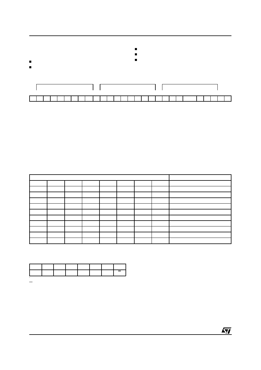
PQFP44 and TQFP44
1
2
3
5
6
4
7
8
9
10
17
11
18 19 20 21 22
44 43 42 41
39
40
38 37 36 35 34
28
27
26
24
23
25
33
32
31
29
30
DIFF_R
DIFFGND_R
LOUD_R
IN_R
TREB_R
MUXOUT_R
MONO
STEREO3_R
STEREO2_R
STEREO4_R
STEREO1_R
LOUD_L
DIFFGND_L
DIFF_L
STEREO4_L
STEREO2_L
STEREO1_L
STEREO3_L
CSM
IN_L
MUXOUT_L
MID_LI
TREB-L
AGND
AVDD
DVDD
CREF
ADDR
SCL
SDA
DGND
PAUSE
OUT_LF
SMEXT
BASS_RO
BASS_RI
BASS_LI
MID_LO
BASS_LO
OUT_RF
OUT_LR
MID_RI
OUT_RR
MID_RO
D96AU435A
12 13 14 15 16
PIN CONNECTION
Æ
1/23
ABSOLUTE MAXIMUM RATINGS
Symbol
Parameter
Value
Unit
AV
DD
, DV
DD
Operating Supply Voltage
10.5
V
T
amb
Operating Ambient Temperature
-40 to 85
∞
C
T
stg
Storage Temperature Range
-55 to 150
∞
C
THERMAL DATA
Symbol
Parameter
Value
Unit
R
th j-amb
Thermal Resistance Junction-pins
Max.
150
∞
C/W
QUICK REFERENCE DATA
Symbol
Parameter
Min.
Typ.
Max.
Unit
AV
DD
, DV
DD
Supply Voltage (AV
DD
and DV
DD
must be at the same potential)
6
9
10.2
V
V
CL
Max. input signal handling
2.1
2.6
Vrms
THD
Total Harmonic Distortion V = 1Vrms f = 1KHz
0.01
0.8
%
S/N
Signal to Noise Ratio
111
dB
S
C
Channel Separation f = 1KHz
95
dB
Input Gain 1dB step
0
15
dB
Volume Control 1dB step
-63
16
dB
Treble Control 2dB step
-14
+14
dB
Bass Control 2dB step
-14
+14
dB
Middle Control 2dB step
-14
+14
dB
Fader and Balance Control 1dB step
-79
0
dB
Loudness Control 1dB step
0
20
dB
Mute Attenuation
100
dB
TDA7437
2/23
STEREOIN1L
SUPPLY
AVDD
ANGND
TREBLE
BASS
MIDDLE
D95AU249B
I2
C
BUS
DECODER
+
LATCHES
SPKR
ATT
SPKR
ATT
TREBLE
BASS
MIDDLE
SPKR
ATT
SPKR
ATT
SDA
RRout
FRout
RLout
FLout
DIFFINR
VOLUME
+
LOUDN
VOLUME
+
LOUDN
MONO
STEREOIN2L
STEREOIN4R
ADDR
SCL
DIGGND
S-MUTE
S-MUTE
MUTE
CONTROL
SOFT,
ZERO
CSM
PAUSE
SMEXT
BIN(R)
BOUT(R)
MIN(R)
MOUT
(R)
TREBLE(R)
CREF
LOUD(R)
INGAIN
MULTIPLEXER
INGAIN
LOUD(L)
STEREOIN3L
STEREOIN4L
DIFFINL
DIFFINLGND
STEREOIN1R
STEREOIN2R
STEREOIN3R
DIFFINRGND
BIN(L)
BOUT(L)
MIN(L)
MOUT(L)
TREBLE(L)
MUXOUT_L
IN_L
MUXOUT_R
IN_R
4
x
470nF
2
x
4.7
µ
F
2
x
4.7
µ
F
5
x
470nF
DVDD
22
µ
F
2.2
µ
F
2.2
µ
F
47nF
47nF
5.6nF
5.6nF
22nF
2.7K
18nF
100nF
5.6K
100nF
22nF
2.7K
18nF
100nF
5.6K
100nF
47nF
47nF
BLOCK DIAGRAM
TDA7437
3/23

ELECTRICAL CHARACTERISTICS (AV
DD
, DV
DD
= 9V; R
L
= 10K
; R
g
= 50
; T
amb
= 25
∞
C;
all gains = 0dB; f = 1KHz. Refer to the test circuit, unless otherwise specified.)
Symbol
Parameter
Test Condition
Min.
Typ.
Max.
Unit
INPUT SELECTOR (MONO AND STEREO INPUTS)
R
I
Input Resistance
pin 7 to 11 and 15 to 18
70
100
130
K
V
CL
Clipping Level
d
0.3%
2.1
2.6
V
RMS
S
I
Input Separation
80
95
dB
R
L
Output Load Resistance
2
K
G
I MIN
Minimum Input Gain
-0.75
0
+0.75
dB
G
I MAX
Maximum Input Gain
14
15
16
dB
G
step
Step Resolution
0.5
1.0
1.5
dB
E
a
Set Error
-1.0
0
1.0
dB
V
DC
DC Steps
Adiacent Gain Steps
0.5
10
mV
G
IMIN
to G
IMAX
3
mV
DIFFERENTIAL INPUT (Pin 5, 6, 13, 14)
R
I
Input Resistance
Input selector BIT D4 = 0 (0dB)
10
15
20
K
Input selector BIT D4 = 1(-6dB)
14
20
26
K
CMRR
Common Mode Rejection Ratio
V
CM
= 1V
RMS
;
f =1KHz
45
70
dB
d
Distortion
V
I
= 1V
RMS
0.01
0.08
%
e
IN
Input Noise
20Hz to 20KHz; Flat; D6 = 0
5
µ
V
G
DIFF
Differential Gain
D4 = 0
-1
0
1
dB
D4 = 1
-7
-6
-5
dB
VOLUME CONTROL
R
I
Input Resistance
Pin 2 and 20
31
44
57
K
G
MAX
Maximum Gain
15
16
17
dB
A
MAX
Maximum Attenuation
61
63.75
66.5
dB
A
STEPC
Step Resolution Coarse Atten.
0.5
1.0
1.5
dB
E
A
Attenuation Set Error
G = 16 to -20dB
-1.0
0
1.0
dB
G = -20 to -63dB
-2.75
2.75
dB
E
t
Tracking Error
2
dB
V
DC
DC Steps
Adjacent Gain Steps
-5
+5
mV
Adjacent Attenuation Steps
-3
+3
mV
From 0dB to A
MAX
0.5
5
mV
LOUDNESS CONTROL (Pin 4, 12)
R
I
Internal Resistor
Loud = On
35
50
65
K
A
MAX
Maximum Attenuation
19
20
21
dB
A
step
Step Resolution
0.5
1
1.5
dB
ZERO CROSSING MUTE
V
TH
Zero Crossing Threshold
(note 1)
WIN = 11
30
mV
WIN = 10
60
mV
WIN = 01
110
mV
WIN = 00
220
mV
A
MUTE
Mute Attenuation
80
100
dB
V
DC
DC Step
0dB to Mute
0.1
3
mV
TDA7437
4/23
ELECTRICAL CHARACTERISTICS (continued)
Symbol
Parameter
Test Condition
Min.
Typ.
Max.
Unit
SOFT MUTE
A
MUTE
Mute Attenuation
50
65
dB
T
DON
ON Delay Time
C
CSM
= 22nF; 0 to -20dB; I = I
MAX
0.8
1.5
2.0
ms
C
CSM
= 22nF; 0 to -20dB; I = I
MIN
25
45
60
ms
T
DOFF
OFF Current
V
CSM
= 0V; I = I
MAX
20
40
60
µ
A
V
CSM
= 0V; I = I
MIN
2
µ
A
R
INT
Pullup Resistor (pin 28)
(note 2)
100
K
V
SMH
(pin 28) Level High
3.5
V
V
SML
(pin 28) Level Low
Soft Mute Active
1
V
BASS CONTROL
C
range
Control Range
±
11.5
±
14
±
16
dB
A
step
Step Resolution
1
2
3
dB
R
g
Internal Feedback Resistance
31
44
57
K
MIDDLE CONTROL
C
range
Control Range
±
11.5
±
14
±
16
dB
A
step
Step Resolution
1
2
3
dB
R
g
Internal Feedback Resistance
17.5
25
32.5
K
TREBLE CONTROL
C
RANGE
Control Range
±
13
±
14
±
15
dB
A
step
Step Resolution
1
2
3
dB
SPEAKER ATTENUATORS
C
RANGE
Control Range
79
dB
A
step
Step Resolution
A
V
= 0 to -40dB
0.5
1
1.5
dB
A
MUTE
Output Mute Attenuation
Data Word = 1111XXXX
80
100
dB
E
A
Attenuation Set Error
A
V
= 0 to -40dB
1.5
dB
V
DC
DC Steps
Adjacent Attenuation Steps
0.1
3
mV
AUDIO OUTPUT
V
clip
Clipping Level
d = 0.3%
2.1
2.6
Vrms
R
L
Output Load Resistance
2
K
R
O
Output Impedance
50
90
140
V
DC
DC Voltage Level
3.5
3.8
4.1
V
TDA7437
5/23
ELECTRICAL CHARACTERISTICS (continued)
Symbol
Parameter
Test Condition
Min.
Typ.
Max.
Unit
PAUSE DETECTOR
V
TH
Pause Threshold
WIN = 11
30
mV
WIN = 10
60
mV
WIN = 01
110
mV
WIN = 00
220
mV
I
DELAY
Pull-Up Current
15
25
35
µ
A
V
THP
Pause Threshold
3.0
V
GENERAL
V
CC
Supply Voltage
6
9
10.2
V
I
CC
Supply Current
7
10
13
mA
PSRR
Power Supply Rejection Ratio
f = 1KHz
70
90
dB
e
NO
Output Noise
Output Muted (B = 20 to 20kHz flat)
4
µ
V
All Gains 0dB
(B= 200 to 20kHz flat)
6
15
µ
V
E
t
Total Tracking Error
A
V
= 0 to -20dB
0
1
dB
A
V
= -20 to -60dB
0
2
dB
S/N
Signal to Noise Ratio
All Gains = 0dB; V
O
= 2.1V
rms
111
dB
S
C
Channel Separation L - R
80
95
dB
d
Distortion
V
IN
=1V all gain = 0dB
0.01
0.08
%
BUS INPUTS
V
IL
Input Low Voltage
1
V
V
lN
Input High Voltage
3
V
I
lN
Input Current
VIN = 0.4V
-5
5
µ
A
V
O
Output Voltage SDA
Acknowledge
I
O
= 1.6mA
0.1
0.4
V
Note 1: WIN represents the MUTE programming bit pair D
6
, D
5
for the zero crossing window threshold
Note 2: Internall pullup resistor to Vs/2; "LOW" = softmute active
Note: The ANGND and DIGGND layout wires must be kept separated. A 50
resistor is recommended to be put as far as possible
from the device.
CD
TDA7437
L-
L+
R-
R+
D00AU1125
L+
L-
R-
R+
=
The CLD - and CDR - can be shortcircuited in applications providing 3 wires CD signal
CLD - = DIFFINLGND
CDR - = DIFFINRGND
TDA7437
6/23

Figure 4: Timing Diagram of I
2
CBUS
Figure 3: Data Validity on the I
2
CBUS
I
2
C BUS INTERFACE
Data transmission from microprocessor to the
TDA7437 and viceversa takes place thru the 2
wires I
2
C BUS interface, consisting of the two
lines SDA and SCL (pull-up resistors to positive
supply voltage must be externally connected).
Data Validity
As shown in fig. 3, the data on the SDA line must
be stable during the high period of the clock. The
HIGH and LOW state of the data line can only
change when the clock signal on the SCL line is
LOW.
Start and Stop Conditions
As shown in fig.4 a start condition is a HIGH to
LOW transition of the SDA line while SCL is
HIGH. The stop condition is a LOW to HIGH tran-
sition of the SDA line while SCL is HIGH.
A STOP conditions must be sent before each
START condition.
Byte Format
Every byte transferred to the SDA line must con-
tain 8 bits. Each byte must be followed by an ac-
knowledge bit. The MSB is transferred first.
Acknowledge
The master (
µ
P) puts a resistive HIGH level on the
SDA line during the acknowledge clock pulse (see
fig. 5). The peripheral (audioprocessor) that ac-
knowledges has to pull-down (LOW) the SDA line
during the acknowledge clock pulse, so that the
SDA line is stable LOW during this clock pulse.
The audioprocessor which has been addressed
has to generate an acknowledge after the reception
of each byte, otherwise the SDA line remains at the
HIGH level during the ninth clock pulse time. In this
case the master transmitter can generate the
STOP information in order to abort the transfer.
Transmission without Acknowledge
Avoiding to detect the acknowledge of the audio-
processor, the
µ
P can use a simplier transmis-
sion: simply it waits one clock without checking
the slave acknowledging, and sends the new
data.
This approach of course is less protected from
misworking and decreases the noise immunity.
Figure 5: Acknowledge on the I
2
CBUS
TDA7437
7/23
MSB
LSB
FUNCTION
X
X
X
I
A3
A2
A1
A0
0
0
0
0
Input Selector
0
0
0
1
Loudness
0
0
1
0
Volume
0
0
1
1
Bass, Treble
0
1
0
0
Speaker Attenuator LF
0
1
0
1
Speaker Attenuator LR
0
1
1
0
Speaker Attenuator RF
0
1
1
1
Speaker Attenuator RR
1
0
0
0
Input Gain Middle
1
0
0
1
Mute
AUTO INCREMENT
If bit I in the subaddress byte is set to "1", the autoincrement of the subaddress is enabled
SUBADDRESS (receive mode)
TRANSMITTED DATA
Send Mode
MSB
LSB
X
X
X
X
X
SM
ZM
P
P = Pause (Active low)
ZM = Zero crossing muted (HIGH active)
SM = Soft mute activated (HIGH active)
X = Not used
The transmitted data is automatically updated after each ACK.
Transmission can be repeated without new chipaddress.
SOFTWARE SPECIFICATION
Interface Protocol
The interface protocol comprises:
A start condition (s)
A chip address byte,(the LSB bit determines
read (=1)/write (=0) transmission)
A subaddress byte.
A sequence of data (N-bytes + acknowledge)
A stop condition (P)
CHIP ADDRESS
SUBADDRESS
DATA 1 to DATA n
MSB
LSB
MSB
LSB
MSB
LSB
S
1
0
0
0
1
0
A R/W
ACK
X
X
X
I
A3 A2 A1 A0
ACK
DATA
ACK
P
ACK = Acknowledge
S = Start
P = Stop
I = Auto Increment
X = Not used
MAX CLOCK SPEED 500kbits/s
ADDRpin open
A = 0
ADDRpin close to Vs A = 1
TDA7437
8/23

DATA BYTE SPECIFICATION
MSB
LSB
FUNCTION
D7
D6
D5
D4
D3
D2
D1
D0
1
0
0
0
DIFFERENTIAL
1
0
0
1
STEREO 1
1
0
1
0
STEREO 2
1
0
1
1
STEREO 3
1
1
0
0
STEREO 4
1
1
0
1
MONO
X
X
X
X
0
X
X
X
DC CONNECT (1)
0
0
HALF-DIFF 0dB (*)
0
1
HALF-DIFF -6dB (*)
1
0
FULL-DIFF 0dB (**)
1
1
FULL-DIFF -6dB (**)
(*) Selected when using a 3 wires differential source (pins 5 and 13 shorted)
(**) Selected when using 4 wires differential source
(1) OUTR-INR (OUTL-INR) short circuited internally (no need external connection)
Input Selector
MSB
LSB
FUNCTION
D7
D6
D5
D4
D3
D2
D1
D0
LOUDNESS STEP
0
0
0
0
0
0
0dB
0
0
0
0
0
1
1dB
0
0
0
0
1
0
2dB
0
0
0
0
1
1
3dB
0
0
0
1
0
0
4dB
0
0
0
1
0
1
5dB
0
0
0
1
1
0
6dB
0
0
0
1
1
1
7dB
0
0
1
0
0
0
8dB
0
0
1
0
0
1
9dB
0
0
1
0
1
0
10dB
0
0
1
0
1
1
11dB
0
0
1
1
0
0
12dB
0
0
1
1
0
1
13dB
0
0
1
1
1
0
14dB
0
0
1
1
1
1
15dB
0
1
0
0
0
0
16dB
0
1
0
0
0
1
17dB
0
1
0
0
1
0
18dB
0
1
0
0
1
1
19dB
0
1
0
1
0
0
20dB
1
LOUDNESS OFF
FINE VOLUME
0
0
0dB
0
1
-0.25dB
1
0
-0.5dB
1
1
-0.75dB
Loudness
TDA7437
9/23

MSB
LSB
FUNCTION
D7
D6
D5
D4
D3
D2
D1
D0
0
1
Soft Mute On
0
0
1
Soft Mute with fast slope
0
1
1
Soft Mute with slow slope
0
0
1
Zero Mute
1
Direct Mute
1
Reset
0
0
0
Zerocross window (220mV)
0
1
0
Zerocross window (110mV)
1
0
0
Zerocross window (60mV)
1
1
0
Zerocross window (30mV)
0
Nonsymmetrical Bass
1
Symmetrical Bass
Mute
MSB
LSB
FUNCTION
D7
D6
D5
D4
D3
D2
D1
D0
1
0
0
0
0dB
1
0
0
1
-1dB
1
0
1
0
-2dB
1
0
1
1
-3dB
1
1
0
0
-4dB
1
1
0
1
-5dB
1
1
1
0
-6dB
1
1
1
1
-7dB
1
1
0
0
0
0
16dB
1
0
0
0
1
8dB
1
0
0
1
0
0dB
1
0
0
1
1
-8dB
1
0
1
0
0
-16dB
1
0
1
0
1
-24dB
1
0
1
1
0
-32dB
1
0
1
1
1
-40dB
1
1
0
0
0
-48dB
1
1
0
0
1
-56dB
0
X
X
X
X
X
X
X
MUTE
Volume
TDA7437
10/23

MSB
LSB
FUNCTION
D7
D6
D5
D4
D3
D2
D1
D0
1.25dB step
0
0
0
0dB
0
0
1
-1dB
0
1
0
-2dB
0
1
1
-3dB
1
0
0
-4dB
1
0
1
-5dB
1
1
0
-6dB
1
1
1
-7dB
0
0
0
0
0dB
0
0
0
1
-8dB
0
0
1
0
-16dB
0
0
1
1
-24dB
0
1
0
0
-32dB
0
1
0
1
-40dB
0
1
1
0
-48dB
0
1
1
1
-56dB
1
0
0
0
-64dB
1
0
0
1
-72dB
1
1
1
1
X
X
X
MUTE
Speaker
TDA7437
11/23

MSB
LSB
FUNCTION
D7
D6
D5
D4
D3
D2
D1
D0
TREBLE STEP
0
0
0
0
-14dB
0
0
0
1
-12dB
0
0
1
0
-10dB
0
0
1
1
-8dB
0
1
0
0
-6dB
0
1
0
1
-4dB
0
1
1
0
-2dB
0
1
1
1
0dB
1
1
1
1
0dB
1
1
1
0
2dB
1
1
0
1
4dB
1
1
0
0
6dB
1
0
1
1
8dB
1
0
1
0
10dB
1
0
0
1
12dB
1
0
0
0
14dB
BASS STEPS
0
0
0
0
-14dB
0
0
0
1
-12dB
0
0
1
0
-10dB
0
0
1
1
-8dB
0
1
0
0
-6dB
0
1
0
1
-4dB
0
1
1
0
-2dB
0
1
1
1
0dB
1
1
1
1
0dB
1
1
1
0
2dB
1
1
0
1
4dB
1
1
0
0
6dB
1
0
1
1
8dB
1
0
1
0
10dB
1
0
0
1
126B
1
0
0
0
14dB
Bass Treble
TDA7437
12/23

MSB
LSB
FUNCTION
D7
D6
D5
D4
D3
D2
D1
D0
IN-GAIN STEP
0
0
0
0
0dB
0
0
0
1
1dB
0
0
1
0
2dB
0
0
1
1
3dB
0
1
0
0
4dB
0
1
0
1
5dB
0
1
1
0
6dB
0
1
1
1
7dB
1
0
0
0
8dB
1
0
0
1
9dB
1
0
1
0
10dB
1
0
1
1
11dB
1
1
0
0
12dB
1
1
0
1
13dB
1
1
1
0
14dB
1
1
1
1
15dB
MIDDLE STEP
0
0
0
0
-14dB
0
0
0
1
-12dB
0
0
1
0
-10dB
0
0
1
1
-8dB
0
1
0
0
-6dB
0
1
0
1
-4dB
0
1
1
0
-2dB
0
1
1
1
0dB
1
1
1
1
0dB
1
1
1
0
2dB
1
1
0
1
4dB
1
1
0
0
6dB
1
0
1
1
8dB
1
0
1
0
10dB
1
0
0
1
126B
1
0
0
0
14dB
Input Stage Gain Middle
TDA7437
13/23

MUTE & PAUSE FEATURES
The TDA7437 provides three types of mute, con-
trolled via I2C bus (see pag. 10, MUTE BYTE regis-
ter).
SOFT MUTE
Bit D0=1
Soft Mute ON
Bit D0=0
Soft Mute OFF
It allows an automatic soft muting and unmuting
of the signal.
The time constant is fixed by an external capaci-
tor Csm inserted between pin Csm and ground.
Once fixed the external capacitor, two different
slopes (time constant) are selectable by program-
mation of bit D1.
Bit D1=0
fast slope (I=Imax)
Bit D1=1
slow slope (I=Imin)
The soft mute generates a gradual signal de-
creasing avoiding big click noise of an immediate
high attenuation, without necessity to program a
sequence of decreasing volume levels. A re-
sponse example is reported in Fig.12 (mute) and
Fig.13 (unmute). The final attenuation obtained
with soft mute ON is 60dB typical.
The used reference parameter is the delay time
taken to reach 20dB attenuation (no matter what
the signal level is).
Using a capacitor Csm=22nF this delay is:
d = 1. 8ms when selected Fast slope mode (bit D1=0)
d = 25 ms when selected Slow slope mode (bit D1=1
In application, the soft mute ON programmation
should be followed by programmation of DIRECT
MUTE ON (see later) in order to achieve a final
100dB attenuation.
Beside the I2C bus programmation, the Soft Mute
ON can be generated in a fast way by forcing a
LOW level at pin SMEXT (TTL Level compatible).
This approach is recommended for fast RDS AF
switching.
The Soft Mute status can be detected via I2C
bus, reading the Transmitted Byte, bit SM (see
data sheet pag. 8).
read bit SM = 1 soft mute status ON
read bit SM = 0 soft mute status OFF
DIRECT MUTE
bit D3 = 1 Direct mute ON
bit D3 = 0 Direct nute OFF
The direct mute bit forces an internal immediate
signal connection to ground.
It is located just before the Volume/Loudness
stage, and gives a typical 100dB attenuation.
SPEAKERS MUTE
An additional direct mute function is included in
the speakers attenuators stage.
The four output LF, RF, LR, RR can be separately
muted by setting the speaker attenuator byte to
the value 01111111 binary.
Typical attenuation level 100dB. This mute is use-
ful for fader and balance functions. It should not
be applied for system mute/unmute, because it
can generate noise due to the offset of previous
stages (bass / treble).
ZEROCROSSING MUTE
bit D2=1 D4=0 zero crossing mute ON
bit D2=0 D4=0 zero crossing mute OFF
The mute activation/deactivation is delayed until
the signal waveform crosses the DC zero level
(Vref level).
The detection works separately for the left and
the right channels (see Figg. 14, 15). Four differ-
ent windows threshold are software selectable by
two dedicated bits.
bit D6 bit D5
WINDOW
0
0
Vref DC +/-220mV
0
1
Vref DC +/-110mV
1
0
Vref DC +/-60mV
1
1
Vref DC +/-30mV
The zero crossing mute activation/deactivation
starts when the AC signal level falls inside the se-
lected window (internal comparator).
The ZEROCROSS Mute (and Pause) detector is
always active. It can be disabled, if the feature is
not used, by forcing the bit D4=1 Zero crossing
and Pause detector reset.
In this way the internal comparator logic is
stopped, eliminating its switching noise.
The zero cross mute status is detected reading
the Transmitted Byte bit ZM.
bit ZM = 1 zero cross mute status ON
bit ZM = 0 zero cross mute status OFF
PAUSE FUNCTION
On chip is implemented a pause detector block.
It uses the same 4 windows threshold selectable
for the zero crossing mute, bit D6,D5 byte MUTE
(see above). The detector can be put in OFF by
forcing bit D4=1, otherwise it is active.
The Pause detector info is available at PAUSE
pin. A capacitor must be connected between
PAUSE pin and Ground.
When the incoming signal is detected to be out-
side the selected window, the external capacitor
is discharged. When the signal is inside the win-
dow, the capacitor is integrating up (see Figg.16
and 17).
TDA7437
14/23

a)by reading directly the Pause pin level.
The ON/OFF voltage threshold is 3.0V typical.
Pause OFF = level low (< 3.0V)
Pause ON = level high ( ; 3.0V)
b)by reading via I
2
C bus the Transmitted Byte, bit P
P = 0 pause active.
P = 1 no pause detected.
The external capacitor value fixes the time con-
stant.
The pull up current is 25uV typical
With input signal
Vin = 1Vrm --; Vdc pin pause = 15mV
Vin = 0Vrms --; Vdc pin pause = 5.62V
For example choosing Cpause = 100nF the
charge up constant is about 22ms. Instead with
Cpause = 15nF the charge up constant is about
360us.
The Pause detection is useful in applications like
RDS, to perform noiseless tuning frequeny jumps
avoiding to mute the signal.
NO SYMMETRICAL BASS CUT RESPONSE
bit D7=0 No symmetrical
bit D7=1 Symmetrical
The Bass stage has the option to generate an
unsymmetrical response, for cut mode settings
(bass level from -2db to - 14dB)
For example using a T-type band pass externa
The feature is useful for human ear equalization
in noisy enviroments like cars etc.
See examples in Fig. 18 (symmetrical response)
and Fig. 19 (unsymmetrical response).
TRANSMITTED DATA (SEND MODE)
The TDA7437 allows the reading of four info bits.
The type (Stereo/Mono) of received broadcasting
signal is easily checked and displayed by using
the ST bit.
The P bit check is useful in tuning jumps without
signal muting.
The SM soft mute status becomes active immedi-
ately, when bit D0 is set to 1 (soft mute ON,
MUTE byte) and not when the signal level has
reached the 60 dB final attenuation.
TDA7437 I
2
C BUS PROTOCOL
The protocol is standard I
2
C, using subaddress
byte plus data bytes (see pagg.8 to 13).
The optional Autoincrement mode allows to re-
fresh all the bytes registers with transmission of a
single subaddress, reducing drastically the total
transmission time.
Without autoincrement, subaddress bit I = 0, to
refresh all the bytes registers (10), it is necessary
to transmit 10 times the chip address, the subad-
dress and the data byte.
Working with a 100Kb/s clock speed the total time
would be :
[(9*3+2)*10]bits*10us=2.9ms
Instead using autoincrement mode, subaddress
bit I=1, the total time will be:
(9*12+2)*10us=1.1ms.
The autoincrement mode is useful also to refresh
partially the data. For example to refresh the 4
speakers attenuators it is possible to program the
subaddress Spkr LF (code XX010100), followed
by the data byte of SPKR LF, LR, RF, RR in se-
quence.
Note:
that the autoincrement mode has a module 16
counter, whereas the total used register bytes are
10.
It is not correct to refresh all the 10 bytes starting
from a subaddress different than XX010000.
For example using subaddress XX010010 (vol-
ume) the registers
from Volume to Mute (see
pag. 8) are correctly updated but the next two
transmitted bytes instead to refer to the wanted
Input selector and Loudness are discharged. (the
solution in this case is to send two separated pat-
tern in autoinc mode, the first composed by ad-
dress, subaddress XX010010, 8 data bytes, and
the second composed by address, subaddress
XX010000, 2 data bytes).
With autoincrement disabled, the protocol allows
the transmission in sequence of N data bytes of a
specific register, without necessity to resend each
time the address and subaddress bytes.
This feature can be implemented, for example, if
a gradual Volume change has to be performed
(the MCU has not to send the STOP condition,
keeping active the TDA7437 communication).
bit P = 0
Pause active
bit P = 1
No pause detected
bit ZM = 1
Zero cross mute ON
bit ZM = 0
Zero cross mute OFF
bit SM = 1
Soft mute ON
bit SM = 0
Soft mute OFF
bit ST = 1
Stereo signal detected (input MPX)
bit ST = 0
Mono signal detected (input MPX)
TDA7437
15/23
WARNING
The TDA7437 always needs to receive a STOP
condition, before beginning a new START condi-
tion. The device doesn't recognize a START con-
dition if a previously active communication was
not ended by a STOP condition.
I
2
C BUS READ MODE
The TDA7437 gives to the master a 1 byte
"TRANSMITTED INFO" via I2C bus in read
mode. The read mode is Master activated by
sending the chip address with LSB set to 1, fol-
lowed by acknowledge bit.
The TDA7437 recognizes the request. At the fol-
lowing
master
generated
clocks
bits,
the
TDA7437 issues the TRANSMITTED INFO byte
on the SDA data bus line (MSB transmitted first).
At the nineth clock bit the MCU master can:
- acknowledge the reception, starting in this
way the transmission of another byte from
the TDA7437.
- no acknowledge, stopping the read mode
communication.
LOUDNESS STAGE
The previous SGS-THOMSON audioprocessors
were implementing a fixed loudness response,
only ON/OFF sw programmable.
No possibility to change the loud boost rate at a
certain volume level.
The TDA7437 implements a fully programmable
loudness control in 20 steps of 1dB.
It allows a customized loudness response for
each application.
The external network connected to the loudness
pins LOUD_L and LOUD_R fixes the type of loud-
ness response
1) Simple Capacitor
The loudness effect is only a boost of low fre-
quencies. (see Fig.20)
2)Second order Loudness (boost of low and
high frequencies).
3)Second order decreased type Loudness
(lower boost of low and high frequencies).
4)Second order modified type Loudness (higher
boost of low and high frequencies).
BASS & MID FILTERS
Several bass filter types can be implemented.
Normally it is used the basic T-type Bandpass Filter.
Starting from the filter component values (R1 in-
ternal and R2, C1, C2 external), the centre fre-
quency Fc, the gain Av at max bass boost and
the filter Q factor are computed as follows:
F
c
=
1
2
(
R1
R2
C1
C2
)
A
v
=
R2
C2
+
R2
C1
+
R1
C1
R2
C1
+
R2
C2
Q
=
(
R1
R2
C1
C2
)
R2
C1
+
R2
C2
Viceversa fixed Fc, Av, and R1 (internal typ.+/-
30%), the external component values are:
C1
=
A
v
-
1
2
R1
Q
C2
=
Q
Q
C1
A
v
-
1
-
Q
Q
R2
=
A
v
-
1
-
Q
Q
2
C1
F
c
(
A
v
-
1
)
Q
TREBLE STAGE
The Treble stage is a simple high pass filter which
time constant is fixed by internal resistor (50Kohm
typ) and an external capacitor connected between
pins TREB_R/TREB_L and Ground.
IN-OUT PINS
The multiplexer output is available at OUT_R and
OUT_L pins for optional connection of external
graphic equalizer (TDA7316/TDA7317), surround
chip (TDA7346) etc. The signal is fed in again at
pins IN_L and IN-R. In case of application without
external devices the pins OUT_L/OUT_R and
IN_L/IN_R can be left unconnected if bit D3 byte
input selector is forced = 0 (DC connect) instead if
bit D3 is kept = 1 an external decoupling capacitor
must be
provided between OUTR/INR and
OUTL/INR necessary to avoid signal DC jumps,
generating "Clicking" output noise.
The input impedance of the next volume stage is
44Kohm typical (minimum 31Kohm). A capacitor
no lower than 1
µ
F should be used.
INPUT SELECTOR
The multiplexer selector can choose one of the
following inputs:
- a differential CD stereo input.
- a mono input.
- four stereo input
The signal fed to the input pins must be decou-
pled via series capacitors. The minimum allowed
value depends on the correspondent input imped-
ance. For the CD diff input (Zi=10Kohm worst
case ) a Cin=4.7uF is recommended.
TDA7437
16/23

BWL
TIME
0.5s/DIV
CREF
OUT LF
1
2
V
(1V/div)
D95AU380
Figure 8: Power on Time Constant vs Cref
Capacitor C
REF
=4.7
µ
F
BWL
TIME
0.5s/DIV
CREF
OUT LF
1
2
V
(1V/div)
D95AU381
Figure 9: Power on Time Constant vs Cref
Capacitor C
REF
=10
µ
F
BWL
TIME
1s/DIV
CREF
OUT LF
1
2
V
(1V)
D95AU382
Figure 10: Power on Time Constant vs Cref Ca-
pacitor C
REF
=22
µ
F
10
100
1K
10K
Freq(Hz)
-100
-90
-80
-70
-60
-50
-40
S
VRR
(dB)
D95AU383
4.7
µ
F
10
µ
F
22
µ
F
47
µ
F
VS=8V
Ripple=0.2VRMS
AV=-15dB
Figure 11: SVRR vs. Frequency
SOFT MUTE
CH1 9V DC
CH1 0.5V
x
~
CH2 20mV
x
~
CH3 0.2V
x
=
CH4 20mV
x
= T/div 1ms
Chan 2
1ms 0.2V
Chan 3
1ms 2V
SOFT MUTE=ON SLOPE=FAST Vout=500mVrms
D95AU384
TIME
Vout
Pin Csm
Main Menu
V
V
10
10
10
10
Figure 12: Soft Mute ON
TDA7437
17/23

D95AU389
RIGHT
CH2 528mV DC
x Chan 1
0.5ms 0.2V
x Chan 2
0.5ms 0.2V
ZERO CROSSING MUTE = ON
Return
Panel
STATUS
Memory
Save
PANEL
Recall
Auxiliary
Setups
Memory
Card
X-Y mode
Persistance
mode
V
LEFT
TIME
Figure 14: Zero Crossing Mute ON
Pin Csm
Main Menu
V
V
SOFT MUTE=OFF SLOPE=FAST Vout=500mVrms
D95AU387
SOFT MUTE
CH1 9V DC
Chan 2
1ms 0.2V
Chan 1
1ms 2V
Vout
TIME
Figure 13: Soft Mute OFF
D95AU390
2ms
CH1 2.7V DC
x Chan 2
0.2ms 1V
x Chan 1
0.2ms 0.5V
ZERO CROSSING MUTE = OFF
Main Menu
Multi Zoom
off
LEFT
RIGHT
V
TIME
Figure 15: Zero Crossing Mute OFF
Chan 1
20ms 0.2V
Chan 2
20ms 2V
PAUSE DETECTOR ZCW=160mV Cpause=100nF
Main Menu
D95AU391
CH2 4.12V DC
Vout
V
TIME
Figure 16: Pause Detector
Chan 2
20ms 2V
Chan 3
20ms 0.2V
PAUSE DETECTOR ZCW=160mV Cpause=100nF
Main Menu
D95AU392
CH2 4.08V DC
CH1 20mV
x
~
CH2 0.2V
x
=
CH3 20mV
x
~
CH4 5mV
x
~ T/div 20ms
10
10
10
10
Vout
BWL
Figure 17: Pause Detector
TDA7437
18/23

D95AU393
10
100
1K
10K
Freq(Hz)
-15
-10
-5
0
5
10
(dB)
Figure 18: Sym _Bass
D95AU394
10
100
1K
10K
Freq(Hz)
-25
-20
-15
-10
-5
0
5
10
ATT
(dB)
Figure 19: Non_Sym _Bass
D98AU887
10
100
1K
10K
Freq(Hz)
0
2
4
6
8
10
12
14
16
18
ATT
(dB)
Figure 20: Loudness
TDA7437
19/23

C20 5.6nF
TRR
1
2
3
IN_R
O_R
C21
2.2
µ
F
C22 4.7nF
LOUDR
4
C23 4.7
µ
F
5
DIFG_R
C24 4.7
µ
F
6
DIFF_R
C25 470nF
7
ST4_R
C26 470nF
8
ST1_R
C27 470nF
9
ST2_R
C28 470nF
10
ST3_R
C29 470nF
11
MONO
DIFG_R
DIFF_R
ST4_R
ST1_R
ST2_R
ST3_R
MONO
CON4
C30 4.7nF
LOUDR
12
13
DIFG_R
C31 4.7
µ
F
14
DIFF_R
C32 4.7
µ
F
15
ST4_R
C33 470nF
16
ST1_R
C34 470nF
17
ST2_R
C35 470nF
18
ST3_R
DIFG_L
DIFF_L
ST4_L
ST1_L
ST2_L
ST3_L
CON5
C36 470nF
19
CSM
20
21
O_L
C2
2.2
µ
F
I_L
C14
34
OUTLF
C13
33
RF
C12
32
LR
C9
29
OUTRR
LF
RF
LR
RR
GND
CON3
JP3
28
36
DGND
SMEX
37
38
SDA
SCL
CON2
DGND
SDA
SMEX
SCL
JP1
JP2
GND V
CC
CON1
C1
2.2nF
C15
10
µ
F
PAUSE
35
44
TRL
AGND
43
AVDD
42
DVDD
41
ADDR
40
31
MIDRI
30
MIDRO
27
BASSRO
26
BASSRI
23
MIDLO
22
MIDLI
C11
18nF
C10
22nF
C8
100nF
C7
100nF
C4 22nF
C3 18nF
25
BASSLO
24
BASSLI
C6 100nF
C5 100nF
CREF
39
C16 22
µ
F
C17
22
µ
F
C18
100nF
C19
5.6nF
R4
2.7K
R3
5.6K
R2
5.6K
R1
2.7K
D98AU882
R5
50
TEST BOARD DIAGRAM
TDA7437
20/23
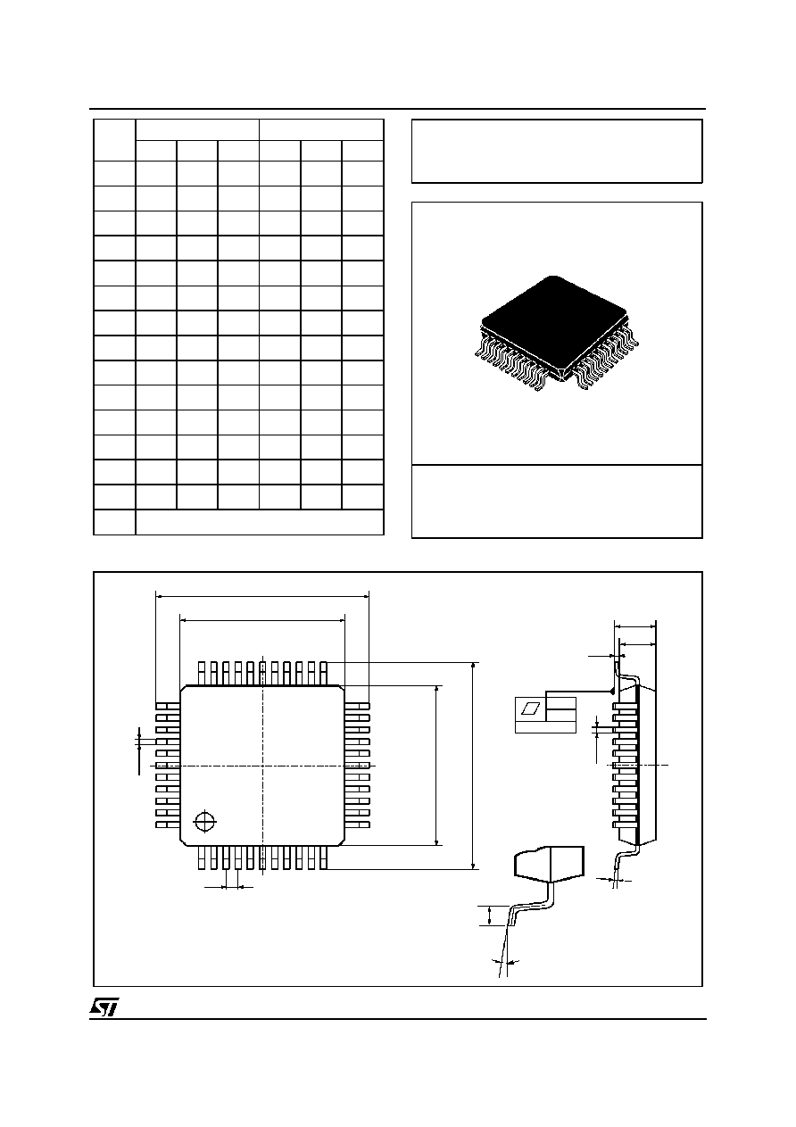
TQFP44 (10 x 10)
DIM.
mm
inch
MIN.
TYP.
MAX.
MIN.
TYP.
MAX.
A
1.60
0.063
A1
0.05
0.15
0.002
0.006
A2
1.35
1.40
1.45
0.053
0.055
0.057
B
0.30
0.37
0.45
0.012
0.014
0.018
C
0.09
0.20
0.004
0.008
D
12.00
0.472
D1
10.00
0.394
D3
8.00
0.315
e
0.80
0.031
E
12.00
0.472
E1
10.00
0.394
E3
8.00
0.315
L
0.45
0.60
0.75
0.018
0.024
0.030
L1
1.00
0.039
K
0∞
(min.), 3.5
∞
(typ.), 7
∞
(max.)
A
A2
A1
B
Seating Plane
C
11
12
22
23
33
34
44
E1
E
D1
D
e
1
K
B
TQFP4410
L
0.10mm
.004
OUTLINE AND
MECHANICAL DATA
TDA7437
21/23

PQFP44 (10 x 10)
A
A2
A1
B
Seating Plane
C
11
12
22
23
33
34
44
E3
D3
E1
E
D1
D
e
1
K
B
PQFP44
L
L1
0.10mm
.004
DIM.
mm
inch
MIN.
TYP.
MAX.
MIN.
TYP.
MAX.
A
2.45
0.096
A1
0.25
0.010
A2
1.95
2.00
2.10
0.077
0.079
0.083
B
0.30
0.45
0.012
0.018
c
0.13
0.23
0.005
0.009
D
12.95
13.20
13.45
0.51
0.52
0.53
D1
9.90
10.00
10.10
0.390
0.394
0.398
D3
8.00
0.315
e
0.80
0.031
E
12.95
13.20
13.45
0.510
0.520
0.530
E1
9.90
10.00
10.10
0.390
0.394
0.398
E3
8.00
0.315
L
0.65
0.80
0.95
0.026
0.031
0.037
L1
1.60
0.063
K
0
∞
(min.), 7
∞
(max.)
OUTLINE AND
MECHANICAL DATA
TDA7437
22/23

Purchase of I
2
C Components of STMicrolectronics, conveys a license under the Philips I
2
C Patent
Rights to use these components in an I
2
C system, provided that the system conforms to the I
2
C
Standard Specifications as defined by Philips.
Information furnished is believed to be accurate and reliable. However, STMicroelectronics assumes no responsibility for the consequences
of use of such information nor for any infringement of patents or other rights of third parti es which may result from its use. No license is
granted by implication or otherwise under any patent or patent rights of STMicroelectronics. Specification mentioned in this publication are
subject to change without notice. This publication supersedes and replaces all information previously supplied. STMicroelectronics products
are not authorized for use as critical components in life support devices or systems without express written approval of STMicroelectronics.
The ST logo is a registered trademark of STMicroelectronics
©
1999 STMicroelectronics ≠ Printed in Italy ≠ All Rights Reserved
STMicroelectronics GROUP OF COMPANIES
Australia - Brazil - China - Finland - France - Germany - Hong Kong - India - Italy - Japan - Malaysia - Malta - Morocco -
Singapore - Spain - Sweden - Switzerland - United Kingdom - U.S.A.
http://www.st.com
TDA7437
23/23