1/9
TDA7535
July 2003
s
20-bit resolution single ended output
s
Analog reconstruction third order Chebyshev filter
s
I2S input data format
s
On chip PLL
s
System clock: 64 Fs
s
2 output channels
s
0.9 VRMS single ended output dynamic
s
3.3V power supply
s
Reset
s
Sampling rate 36KHz to 48KHz
DESCRIPTION
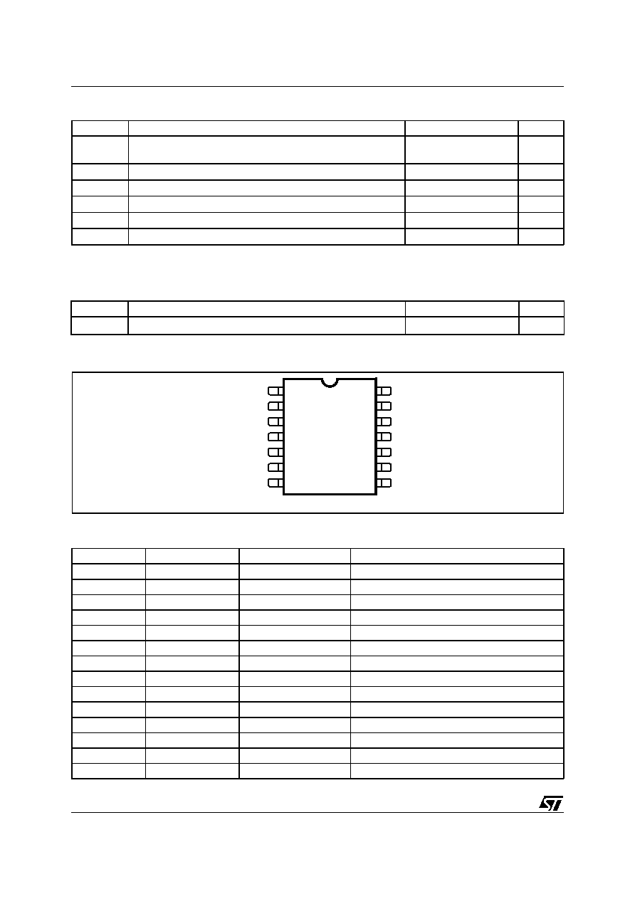
The TDA7535 is a stereo, digital-to-analog converter
designed for audio application, including digital inter-
polation filter, a third order multibit Delta-Sigma DAC,
a third order Chebyshev's reconstruction filter and a
differential to single ended output converter. This de-
vice is fabricated in highly advanced CMOS, where
high speed precision analog circuits are combined
with high density logic circuits. The TDA7535, ac-
cording to standard audio converters, can accept any
I
2
S data format.
The TDA7535 is available in SO-14 and TSSOP-14
packages. The total power consumption is less than
75mW.
TDA7535 is suitable for a wide variety of applications
where high performance are required. Its low cost
and single 3.3V power supply make it ideal for sever-
al applications, such as CD players, MPEG audio,
MIDI applications, CD-ROM drives, CD-Interactive,
digital radio applications and so on. An evaluation
board is available to perform measurement and to
make listening tests.
TSSOP-14
SO-14
ORDERING NUMBER: TDA7535
DELTA/SIGMA CASCADE 20 BIT STEREO DAC
BLOCK DIAGRAM
FIR1
FIR2
ALU
S&H
I
2
S
I
2
S
PLL
CLKOUT
DIGITAL
INPUT 20
FIR3
20
4
MODULATOR
THERMO DECODER &
RANDOMIZER
3rd CHEBYSHEV
SC FILTER
DIFF TO SINGLE
CONVERTER
ANALOG
OUTPUT
F
S
8F
S
23
64F
S
D02AU1417
TDA7535
2/9
ABSOLUTE MAXIMUM RATINGS
Warning: Operation at or beyond these limit may result in permanent damage to the device. Normal operation is not guaranteed at these
extremes.
THERMAL DATA
Note: 1. In still air
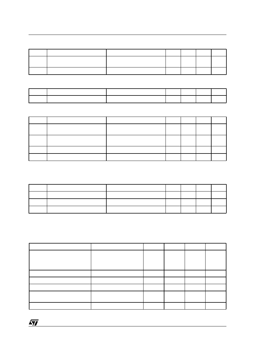
PIN CONNECTIONS (Top views)
PIN FUNCTION (SO14/TSSOP14)
Symbol
Parameter
Value
Unit
V
DD
V
CC
Power supplies
Digital
Analog
-0.5 to +4.6
-0.5 to +4.6
V
V
V
aio
Analog Input and Output Voltage
-0.5 to (V
CC
+0.5)
V
V
dio
Digital Input and Output Voltage
-0.5 to (V
DD
+0.5)
V
V
di5
Digital Input Voltage (5V tolerant)
-0.5 to 6.5
V
T
j
Operating Junction Temperature Range
-40 to 125
�C
T
stg
Storage Temperature
-55 to 150
�C
Symbol
Parameter
Value
Unit
R
th j-amb
Thermal resistance junction to ambient
(1)
85
�C/W
Pin Number
Pin Name
Input/Output Power
Description
1
N.C.
-
-
2
SDATA
I
I2S Digital Data Input
3
SCK
I
I2S Clock Input
4
N.C.
-
-
5
GND_DIG
P
Digital Ground
6
GND_ANA
P
Analog Ground
7
OUTSR
O
Right Channel single ended Output
8
OUTSL
O
Left Channel single ended Output
9
VCM
P
Reference 1.65V externally filtered
10
VDD_ANA
P
Analog 3.3V-Supply
11
N.C.
-
-
12
VDD_DIG
P
Digital 3.3V-Supply
13
FSYNC
I
I2S Left-Right Channel selector
14
RESETN
I
Reset (active low)
N.C.
SDATA
SCK
N.C.
GND_DIG
OUTSR
GND_ANA
OUTSL
VDD_ANA
VCM
N.C.
VDD_DIG
FSYNC
RESETN
1
3
2
4
5
6
7
12
11
10
9
8
13
14
D01AU1276A
3/9
TDA7535
RECOMMENDED DC OPERATING CONDITIONS
POWER CONSUMPTION
GENERAL INTERFACE ELECTRICAL CHARACTERISTICS
Note: 1. The leakage currents are generally very small, <1nA. The value given here, 1mA, is the maximum that can occur after an Electro-
static Stress on the pin.
2. Human Body Model.
LOW VOLTAGE CMOS INTERFACE DC ELECTRICAL CHARACTERISTICS
Symbol
Parameter
Test Condition
Min.
Typ.
Max.
Unit
V
DD
3.3V Digital Power Supply
Voltage
3.15
3.3
3.45
V
V
CC
3.3V Analog Power Supply Voltage
3.15
3.3
3.45
V
Symbol
Parameter
Test Condition
Min.
Typ.
Max.
Unit
I
dd
Total Maximum Current
power supply @ 3.3V and T
j
= 125�C
21.5
25
mA
Symbol
Parameter
Test Condition
Min.
Typ.
Max.
Unit
l
il
Low Level Input Current without
pullup device
V
i
= 0V (note 1)
1
�
A
l
ih
High Level Input Current without
pullup device
V
i
= V
dd
(note 1)
1
�
A
I
latchup
I/O latch-up current
V < 0V, V > V
dd
200
mA
V
esd
Electrostatic Protection
Leakage , 1
�
A (note 2)
2000
V
Symbol
Parameter
Test Condition
Min.
Typ.
Max.
Unit
V
il
Low Level Input Voltage
0.2*V
dd
V
V
ih
High Level Input Voltage
0.8*V
dd
V
V
hyst
Schmitt trigger hysteresis
0.8
V
DAC ELECTRICAL CHARACTERISTICS
Vdd = 3.3V; Tamb = 25�C; Input signal frequency = sinus wave generated by Audio Precision Sys.2; Input
Signal Amplitude = see notes; Noise Integration Bandwidth = 20Hz to 22KHz (A- weighted)
Parameter
Test Condition
Min.
Typ.
Max.
Unit
Noise + Distortion
(see note 1)
@0dB
@-6dBb
@-40dB
@-60dB
89
94
96
96
dB
dB
dB
dB
Total Harmonic Distortion
see note 2
94
dB
Dynamic range
see note 3
96
dB
Crosstalk
see note 4
-95
dB
Full Scale Output Voltage
V
dd
= 3.15 to 3.45V
Full scale input
0.8
0.9
1.0
Vrms
Input Sampling Rate
36
48
kHz
TDA7535
4/9
Note1:
It is the ratio between the maximum input signal and the integration of the in-band noise after deducing the power of signal funda-
mental. It depends on the input signal amplitude. In this case 0dB means full scale digital, 1kHz frequency used.
Note 2:
It is the ratio of the rms value of the signal fundamental component at 0dB (full scale digital) to the rms value of all of the harmonic
components in the band.
Note 3:
measured using the SNR at -60dB input signal, with 60dB added to compensate for small input signal.
Note 4:
Left channel on with 0dB/1kHz input signal, Right channel on with DC input signal.
Figure 1. I
2
S interface Diagram
Passband Ripple
0.12
dB
Stopband
@ 3dB
@ 90dB
44.1kHz Sampling Rate
21.53
24.80
kHz
Interchannel Gain Mismatch
0.05
0.1
dB
DAC ELECTRICAL CHARACTERISTICS (continued)
Vdd = 3.3V; Tamb = 25�C; Input signal frequency = sinus wave generated by Audio Precision Sys.2; Input
Signal Amplitude = see notes; Noise Integration Bandwidth = 20Hz to 22KHz (A- weighted)
Parameter
Test Condition
Min.
Typ.
Max.
Unit
FSYNC
SDATA
SCK
32 * SCK
32 * SCK
20 Bits
MSB
LSB
20 Bits
MSB
LSB
Left
Right

5/9
TDA7535
Figure 2. I
2
S Timings
(1)
SCK clock defines the Fs, being the Sample Rate. This input clock needs a jitter below ~212ps
RMS
(2)
FSYNC switches inside the time window as specified w.r.t. to falling edge of SCK
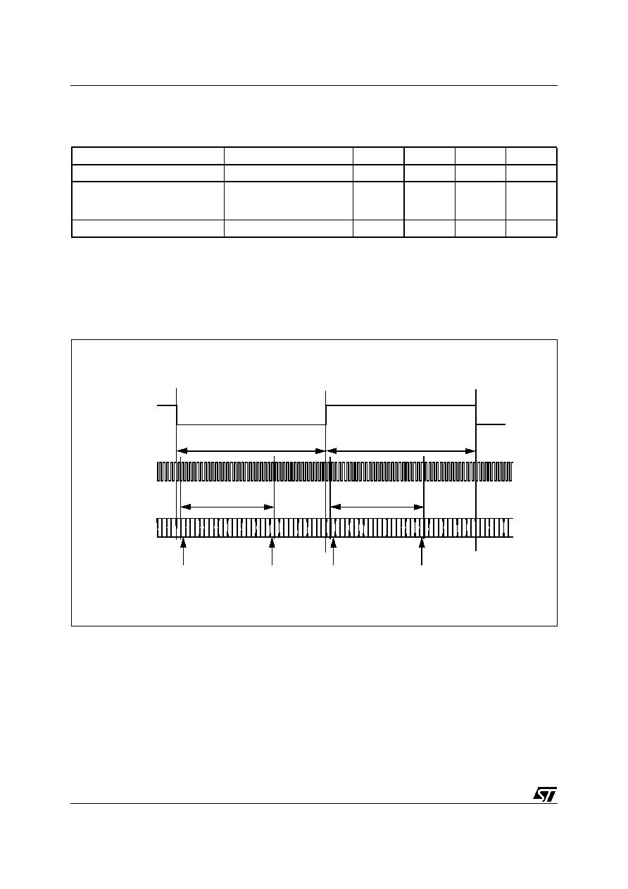
Figure 3. Power Up & Reset Sequence
I
2
S bit clock (SCK) must be present 20ms before reset release to allow PLL locking.
Timing
Description
Minimum
Maximum
Unit
t
sck
Clock Cycle
(1)
1/(64*Fs) -
150ps
RMS
1/(64*Fs) +
150ps
RMS
ns
t
sckpl
SCK Phase Low
0.5*t
sck
- 1%
0.5*t
sck
+1%
ns
t
sckph
SCK Phase High
0.5*t
sck
- 1%
0.5*t
sck
+1%
ns
t
lrw-
FSYNC switching time window before SCK falling edge
(2)
0
0.125*t
sck
-10
ns
t
lrw+
FSYNC switching time window after SCK falling edge
(2)
0
0.125*t
sck
-10
ns
t
sds
SDATA setup time
60
ns
t
sdh
SDATA hold time
30
ns
t
sckr
SCK rise time
1.5
ns
t
sckf
SCK fall time
1.5
ns
t
sck
t
sckpl
t
sds
t
lrw-
t
sckph
t
lrw+
t
sdh
Valid
FSYNC
SDATA
SCK
Valid
t
sckf
t
sckr
T
RES
T
RES
Min 50ms
V
DD
RESET
D02AU1418