May 1993
5.1V +12V REGULATOR WITH DISABLE AND RESET
TDA8138
.
OUTPUT CURRENTS UP TO 1A
.
FIXED PRECISION OUTPUT 1 VOLTAGE
5.1V +/- 2%
.
FIXED PRECISION OUTPUT 2 VOLTAGE
12V +/- 2%
.
OUTPUT 1 WITH RESET FACILITY
.
OUTPUT 2 WITH DISABLE BY TTL INPUT
.
SHORT CIRCUIT PROTECTION AT BOTH
OUTPUTS
.
THERMAL PROTECTION
.
LOW DROP OUTPUT VOLTAGE
.
AVAILABLE ALSO IN HEPTAWATT PACKAGE
IN TWO VERSIONS : TDA8138A (DISABLE
ONLY), TDA8138B (RESET ONLY)
DESCRIPTION
The TDA8138 is a monolithic dual positive voltage
regulator designed to provide fixed precision output
voltages of 5.1V and 12V at currents up to 1A.
An internal reset circuit generates a reset pulse
when the output 1 decrease below the regulated
voltage value (for TDA8138 and TDA8138B).
Output 2 can be disabled by TTL input (for
TDA8138 and TDA8138A).
Short circuit and thermal protections are included
in all the versions.
8
1
3
8
-0
1
A
.
EPS
-
8
1
3
8
-0
1
B
.
E
PS
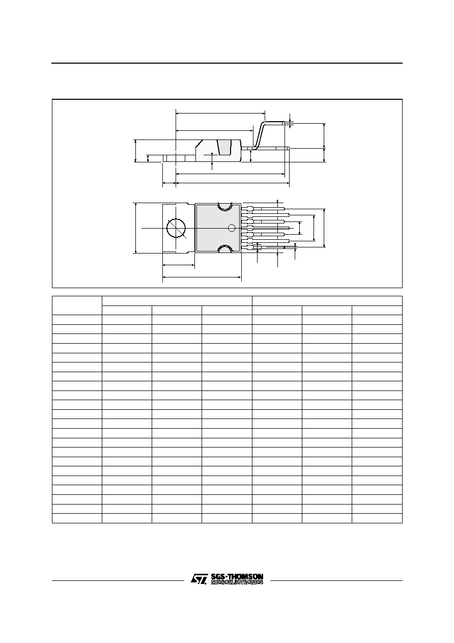
PIN CONNECTIONS
HEPTAWAT
(Plastic Package)
ORDER CODE : TDA8138A / TDA8138B
SIP9
(Plastic Package)
ORDER CODE : TDA8138
OUTPUT1
OUTPUT2
GROUND
INPUT 2
INPUT 1
1
2
3
4
5
6
7
N.C. FOR TDA8138A
RESET FOR TDA8138B
DISABLEFOR TDA8138A
DEL. CAPA FOR TDA8138B
Tab. connected to Pin 4
HEPTAWATT
1
2
3
4
5
6
7
8
9
DEL. CAP.
DISABLE
RESET
N.C.
OUTPUT 2
OUTPUT 1
INPUT 1
INPUT 2
GROUND
Tab. connected to Pin 5
SIP9
1/6
4
5
8
3
9
1
2
6
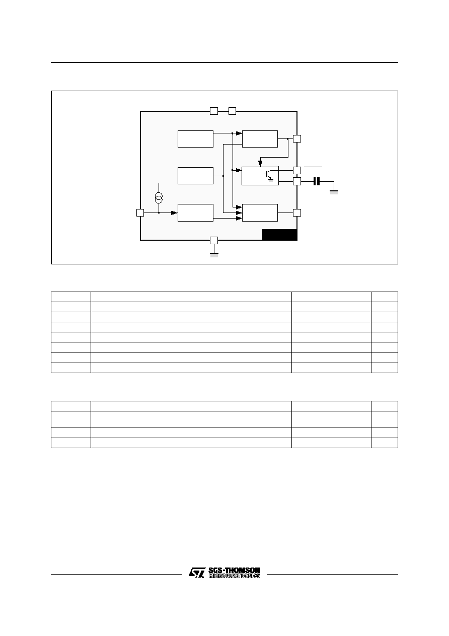
OUT 1
IN 2
IN 1
RESET
OUT 2
DISABLE
DELAY
CAPACITOR
TDA8138
REFERENCE
PROTECTION
DISABLE
OUT 1
OUT 2
RESET
8
1
3
8
-0
2
.
EPS
BLOCK DIAGRAM (SIP9 package)
ABSOLUTE MAXIMUM RATINGS
Symbol
Parameter
Value
Unit
V
IN
DC Input Voltage Pin 1
20
V
V
DIS
Disable Input Voltage Pin 3 (Heptawatt) or Pin 4 (SIP9)
20
V
V
RST
Output Voltage at Pin 6 (SIP9) or Pin 5 (Heptawatt)
20
V
I
O1, 2
Output Currents
Internally Limited
P
t
Power Dissipation
Internally Limited
T
stg
Storage Temperature
-65 to +150
o
C
T
j
Junction Temperature
0 to +150
o
C
81
38
-
0
1
.
T
B
L
THERMAL DATA
Symbol
Parameter
Value
Unit
R
th (j-c)
Maximum Thermal Resistance Junction-case for SIP9
Maximum Thermal Resistance Junction-case for Heptawatt
8
3
o
C/W
o
C/W
R
th (j-a)
Maximum Thermal Resistance Junction-ambient for SIP9
60
o
C/W
T
j
Maximum Recommended Junction Temperature
130
o
C
81
38
-
0
2.
T
B
L
TDA8138
2/6
ELECTRICAL CHRACTERISTICS (V
IN1
= 7V, V
IN2
= 14V, T
j
= 25
o
C, unless otherwise specified)
Symbol
Parameter
Test Conditions
Min.
Typ.
Max.
Unit
V
O1
Output Voltage
I
O1
= 10mA
5
5.1
5.2
V
V
O2
Output Voltage
I
O2
= 10mA
11.76
12
12.24
V
V
O1
Output Voltage
7V < V
IN1
< 14V
14 < V
IN2
< 18V
5mA < I
O1,2
< 750mA
4.9
5.3
V
V
O2
Output Voltage
11.5
12.5
V
V
IO1,2
Dropout Voltage
I
O1,2
= 750mA
I
O1,2
= 1A
1.4
2
V
V
V
O1,2LI
Line Regulation
7V < V
IN1
< 14V
14 < V
IN2
< 18V
I
O1,2
= 200mA
50
120
mV
mV
V
O1,2LO
Load Regulation
5mA < I
O1
< 0.6A
5mA < I
O2
< 0.6A
100
250
mV
mV
I
Q
Quiescent Current
I
O1
= 10mA
Output 2 Disabled
2
mA
V
O1RST
Reset Thrseshold Voltage
K = V
O1
K - 0.4
K -
0.25
K - 0.1
V
V
RTH
Reset Thrseshold Hysteresis
See circuit description
20
50
75
mV
t
RD
Reset Pulse Delay
C
e
= 100nF
See circuit description
25
ms
V
RL
Saturation Voltage in Reset Condition
I
5
= 5mA
0.4
V
I
RH
Leakage Current in Normal Condition
(at Pin 6 for SIP9 or Pin 5 for Heptawatt)
V
5
= 10V
10
�
A
K
O1,2
Output Voltage Thermal Drift
T
j
= 0 to 125
o
C
K
O
=
V
O
10
6
T
V
O
100
ppm/
o
C
I
O1,2SC
Short Circuit Output Current
V
IN1
= 7V, V
IN2
= 14V
V
IN1,2
= 16V (see Note)
1.6
1
A
A
V
DISH
Disable Voltage High (out 2 active)
2
V
V
DISL
Disable Voltage Low (out 2 disabled)
0.8
V
I
DIS
Disable Bias Current
0V < V
DIS
< 7V
-100
2
�
A
T
jsd
Junction Temperature for Thermal Shut
Down
145
o
C
Note : Safe permanent short-circuit is only guaranteed for input voltages up to 16V.
81
38
-
0
3
.
T
B
L
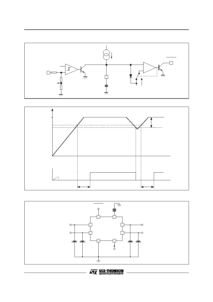
The TDA8138 is a dual voltage regulator with Reset
and Disable (TD8138A : Disable only, TDA8138B :
Reset only).
The two regulation parts are supplied from one
voltage reference circuit trimmed by zener zap
during EWS test.
Since the supply voltage of this last is connected at
Pin 1 (V
IN1
), the regulator 2 will not work if Pin 1 is
not supplied.
The outputs stage have been realized in darlington
configuration with a drop typical 1.2V.
The disable circuit, switch-off the output 2 if a
voltage lower than 0.8V is applied at Pin 3
(Heptawatt) or Pin 4 (SIP9)
The Reset circuit checks the voltage at the out-
put 1. If this one goes below V
OUT
- 0.25V (4.85V
typ.), the comparator "a" (see Figure 1) discharges
rapidly the capacitor C
e
and the reset output goes
at once Low. When the voltage at the out1 rises
above V
OUT
- 0.2V (4.9V typ.), the voltage V
Ce
increases linearly to 2.5V corresponding to a delay
td following the law : t
1
=
C
e
2.5V
10
�
A
(see Figure 2),
then the reset output goes high again. To avoid
gliches in the reset output, the second comparator
"b" has a large hysteresis (1.9V).
CIRCUIT DESCRIPTION
TDA8138
3/6