 | ÐлекÑÑоннÑй компоненÑ: TDA8215B | СкаÑаÑÑ:  PDF PDF  ZIP ZIP |
Äîêóìåíòàöèÿ è îïèñàíèÿ www.docs.chipfind.ru
1/15
May 2004
TDA8215B
HORIZONTAL AND VERTICAL DEFLECTION CIRCUIT
REV. 2
FEATURES SUMMARY
DIRECT LINE DARLINGTON DRIVE
DIRECT FRAME-YOKE DRIVE (± 1A)
COMPOSITE VIDEO SIGNAL INPUT
CAPABILITY
FRAME OUTPUT PROTECTION AGAINST
SHORT CIRCUITS
PLL
VIDEO IDENTIFICATION CIRCUIT
SUPER SANDCASTLE OUTPUT
VERY FEW EXTERNAL COMPONENTS
VERY LOWCOST POWER PACKAGE
DESCRIPTION
The TDA8215B is an horizontal and vertical de-
flection circuit with super sandcastle generator
and video identification output. Used with
TDA8213 (Video & Sound IF system) and
TDA8217 (Pal decoder and video processor), this
IC permits a complete low-cost solution for PAL
applications. The TDA8215B has been specially
designed for direct drive of line DARLINGTON
transistors.
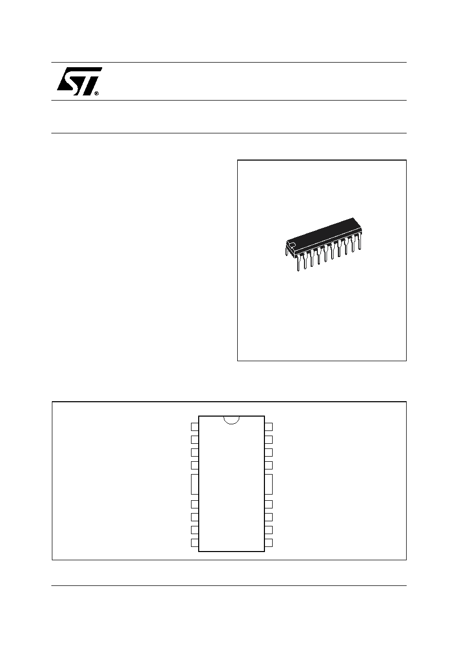
Figure 1. Package
Figure 2. Pin Connections
POWERDIP 16 + 2 + 2
(Plastic Package)
1
20
2
19
3
18
4
17
5
16
6
15
7
14
8
13
9
12
10
VIDEO INPUT
SUPER SANDCASTLE OUTPUT
LINE FLYBACK INPUT
LINE OUTPUT
GROUND
GROUND
RC NETWORK
LINE SAWTOOTH INPUT
PHASE DETECTOR
LINE OSCILLATOR
11
V
CC1
FRAME OSCILLATOR
V
CC2
FRAME FLYBACK GENERATOR
GROUND
GROUND
POWER AMPLIFIER INPUT
VIDEO IDENTIFICATION OUTPUT
FRAME POWER SUPPLY
FRAME OUTPUT
TDA8215B
2/15
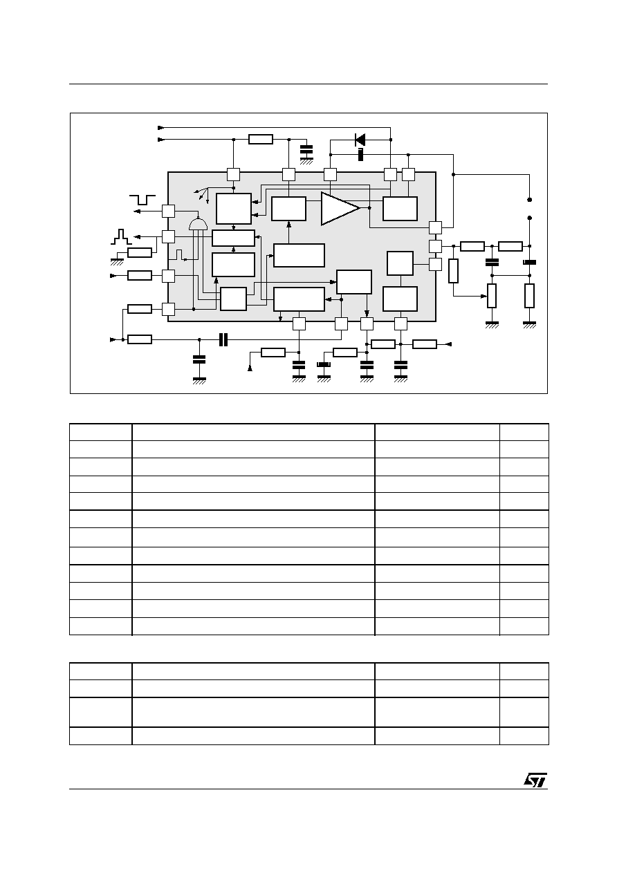
Figure 3. Block Diagram
Table 1. Absolute Maximum Ratings
Table 2. Thermal Data
Symbol
Parameter
Value
Unit
V
CC
1 Supply
Voltage
30
V
V
CC
2
Flyback Generator Supply Voltage
35
V
V9
Frame Power Supply Voltage
60
V
I10
NR
Frame Output Current (non repetitive)
± 1.5
A
I10
Frame Output Current (continuous)
± 1
A
V17
Line Output Voltage (external)
60
V
I
p
17
Line Output Peak Current
0.8
A
I
C
17
Line Output Continuous Current
0.4
A
T
STG
Storage Temperature
40 to 150
°C
T
J
Max Operating Junction Temperature
+ 150
°C
T
AMB
Operating Ambient Temperature
0 to 70
°C
Symbol
Parameter
Value
Unit
R
TH(j-c)
Max Junction-case Thermal Resistance
10
°C/W
R
TH(j-a)
Typical Junction-ambient Thermal Resistance
(Soldered on a 35µm thick 45cm
2
PC Board copper area)
40
°C/W
T
J
Max Recommended Junction Temperature
120
°C
V
CC2
V
CC1
8
19
20
18
Line flyback
detector
Phase
detector
YOKE
Output
stage
Line
oscillator
Frame
blanking
detector
Input
stage
Burst gate pulse
generator
Power
stage
Frame-Synchro
generator
Frame
oscillator
Flyback
generator
14
2µs
2µs
13
12
11
17
7
10
4
3
9
2
1
V
CC1
V
CC1
Video
Identification
Video
Input
Line
Flyback
+
-
3/15
TDA8215B
ELECTRICAL CHARACTERISTICS
V
CC1
= 10V, T
AMB
= 25°C (unless otherwise specified)
Table 3. Supply (Pin 1)
Table 4. Video Input (Pin 20)
Table 5. Line Oscillator (Pin 11)
Table 6. Line Output (Pin 17)
Table 7. Line Sawtooth Input (Pin 13)
Symbol
Parameter
Min.
Typ.
Max.
Unit
I
CC1
Supply Current
15
mA
V
CC1
Supply Voltage
9
10
10.5
V
Symbol
Parameter
Min.
Typ.
Max.
Unit
V20
Reference Voltage (I
20
= -1µA)
1.4
1.75
2
V
MWF
Minimum Width of Frame Pulse (When synchronized with TTL signal)
50
µs
Symbol
Parameter
Min.
Typ.
Max.
Unit
LT11
Low Threshold Voltage
2.8
3.2
3.6
V
HT11
High Threshold Voltage
5.4
6.6
7.8
V
BI11
Bias Current
100
nA
DR11
Discharge Impedance
1.0
1.4
1.8
k
FLP1
Free Running Line Period
(R = 34.9k
Tied to V
CC1
, C = 2.2nF Tied to Ground)
62
64
66
µs
FLP2
Free Running Line Period (R = 13.7K
, C = 2.2nF)
27
µs
OT11
Oscillator Threshold for Line Output Pulse Triggering
4.6
V
Horizontal Frequency Drift with Temperature (see application)
2
Hz/°C
Symbol
Parameter
Min.
Typ.
Max.
Unit
LV17
Saturation Voltage (I
17
= 800mA during 2µs)
2.2
V
OPW
Output Pulse width (line period = 64µs, negative pulse)
19
21
23
µs
Symbol
Parameter
Min.
Typ.
Max.
Unit
V13
Bias Voltage
1.8
2.4
3.2
V
Z13
Input Impedance
4.5
5.8
8
k
F
0
-------
TDA8215B
4/15
Table 8. Phase Detector (Pin 12)
Table 9. Video Identification (Pin 8)
Table 10. Frame Oscillator (Pin 2)
Table 11. Frame Power Supply (Pin 9)
Table 12. Flyback Generator Supply (Pin 3)
Symbol
Parameter
Min.
Typ.
Max.
Unit
I12
Output Current During Synchro Pulse
250
350
500
µA
RI12
Current Ratio (positive/negative)
0.95
1
1.05
LI12
Leakage Current
2
+2
µA
CV12
Control Voltage Range
2.60
7.10
V
Symbol
Parameter
Min.
Typ.
Max.
Unit
Low Level Output when the line synchro tip is centered in the line retrace
V
H8
Without Video Signal (I
8
= -500µA)
4.5
6.3
0.9
V
V
L8
With Video Signal (I
8
= 50µA)
0.6
0.9
V
Symbol
Parameter
Min.
Typ.
Max.
Unit
LT2
Low Threshold Voltage
1.6
2.0
2.3
V
HT2
High Threshold Voltage
2.6
3.1
3.6
V
DIF2
LT2 - HT2
1.0
V
BI2
Bias Current
30
nA
DR2
Discharge Impedance
300
470
700
FFP1
Free Running Frame Period
(R = 845k
Tied to V
CC1
, C = 180nF Tied to Ground)
20.5
23
25
ms
MFP
Minimum Frame Period (I
20
= 100µA) with the Same RC
12.8
ms
FFP2
Free Running Frame Period (R = 408k
, C = 220nF)
14.3
ms
FPR
Frame Period Ratio = FFP/MFP
1.7
1.8
1.9
FG
Frame Saw-tooth Gain Between Pin 1 and non Inverting Input of the
Frame Amplifier
0.4
Vertical Frequency Drift with Temperature (see application)
4.10
3
Hz/°C
Symbol
Parameter
Min.
Typ.
Max.
Unit
V9
Operating Voltage (with flyback Generator)
10
58
V
I9
Supply Current (V9 = 30V)
11
22
m
Symbol
Parameter
Min.
Typ.
Max.
Unit
V
CC
2
Operating Voltage
10
30
V
F
0
-------
5/15
TDA8215B
Table 13. Frame Output (Pin 10)
Table 14. Flyback Generator (Pin 3 and Pin 4)
Table 15. Super Sandcastle Output (Pin 19)
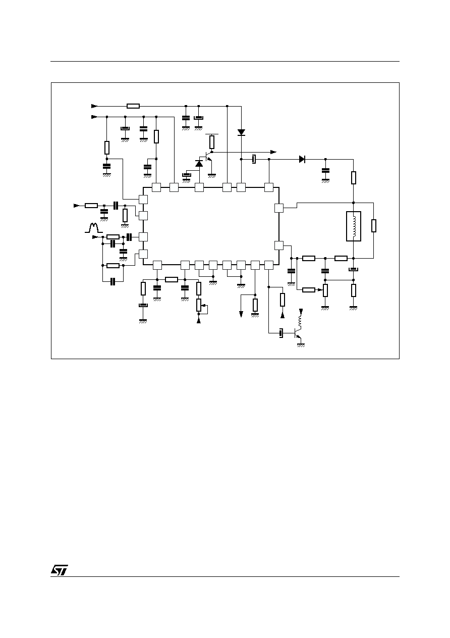
Note: 1. Width of vertical blanking pulse on SSC output is proportional to the frame flyback time, the switching level is V
CC2
-2V
BE
and the
other input of the comparator is tied to the frame amplifier output. Application circuit uses the frame flyback generator.
Symbol
Parameter
Min.
Typ.
Max.
Unit
Saturation Voltage to Ground (V9 = 30V)
LV10A
I10 = 0.1A
0.06
0.6
V
LV10B
I10 = 1A
0.37
1
V
Saturation Voltage to V9 (V9 = 30V)
HV10A
I10 = 0.1A
1.3
1.6
V
HV10B
I10 = 1A
1.7
2.4
V
Saturation Voltage to V9 in Flyback Mode (V10 > V9)
FV10A
I10 = 0.1A
1.6
2.1
V
FV10B
I10 = 1A
2.5
4.5
V
Symbol
Parameter
Min.
Typ.
Max.
Unit
Flyback Transistor on (output = high state), V
CC2
= 30V, V4/3 with
F2DA
I
4
3
= 0.1A
1.5
2.1
V
F2DB
I
4
3
= 1A
3.0
4.5
V
Flyback Transistor on (output = high state), V
CC2
= 30V, V3/4 with
FSVA I
3
4
= 0.1A
0.8
1.1
V
FSVB I
3
4
= 1A
2.2
4.5
V
Flyback Transistor off (output = V9 - 8V), V9 - V
CC2
= 30V
FCI
Leakage Current Pin 3
170
µA
Symbol
Parameter
Min.
Typ.
Max.
Unit
Output Voltages (R load = 2.2k
)
SANDT2 Frame blanking pulse level
2
2.5
3
V
SANDL2 Line blanking pulse level
4
4.5
5
V
BG2
Burst key pulse level
8
9
V
Pulses width and timing
SC3
Delay between middle of sync pulse and leading edge of burst key
pulse
2.3
2.7
3.1
µs
SC2
Duration of burst key pulse
Vertical blanking pulse width
3.7
4
Note 1
5
µs

TDA8215B
6/15
Table 16. Line Flyback Input (Pin 18)
Note: 1. An RC network is connected to this input. Typical value for the resistor is 27k
and 220pF for the capacitor. A different time constant
for RC changes the delay between the middle of the line synchro pulse and the leading edge of the burst key pulse but also the
duration of the burst key pulse.
Symbol
Parameter
Min.
Typ.
Max.
Unit
Switching level
2
V
Maximum input current at V
PEAK
= 800V
8
mA
Limiting voltage at maximum current
4.3
V
RC network time constant (Note 1)
6
µs
7/15
TDA8215B
GENERAL DESCRIPTION
The TDA8215B performs all the video and power
functions required to provide signals for the line
driver and frame yoke.
It contains:
A synchronization separator
An integrated frame separator without external
components
A saw-tooth generator for the frame
A power amplifier for direct drive of frame yoke
(short circuit protected)
An open collector output for the line darlington
drive
A line phase detector and a voltage control
oscillator
A super sandcastle generator
Video identification output.
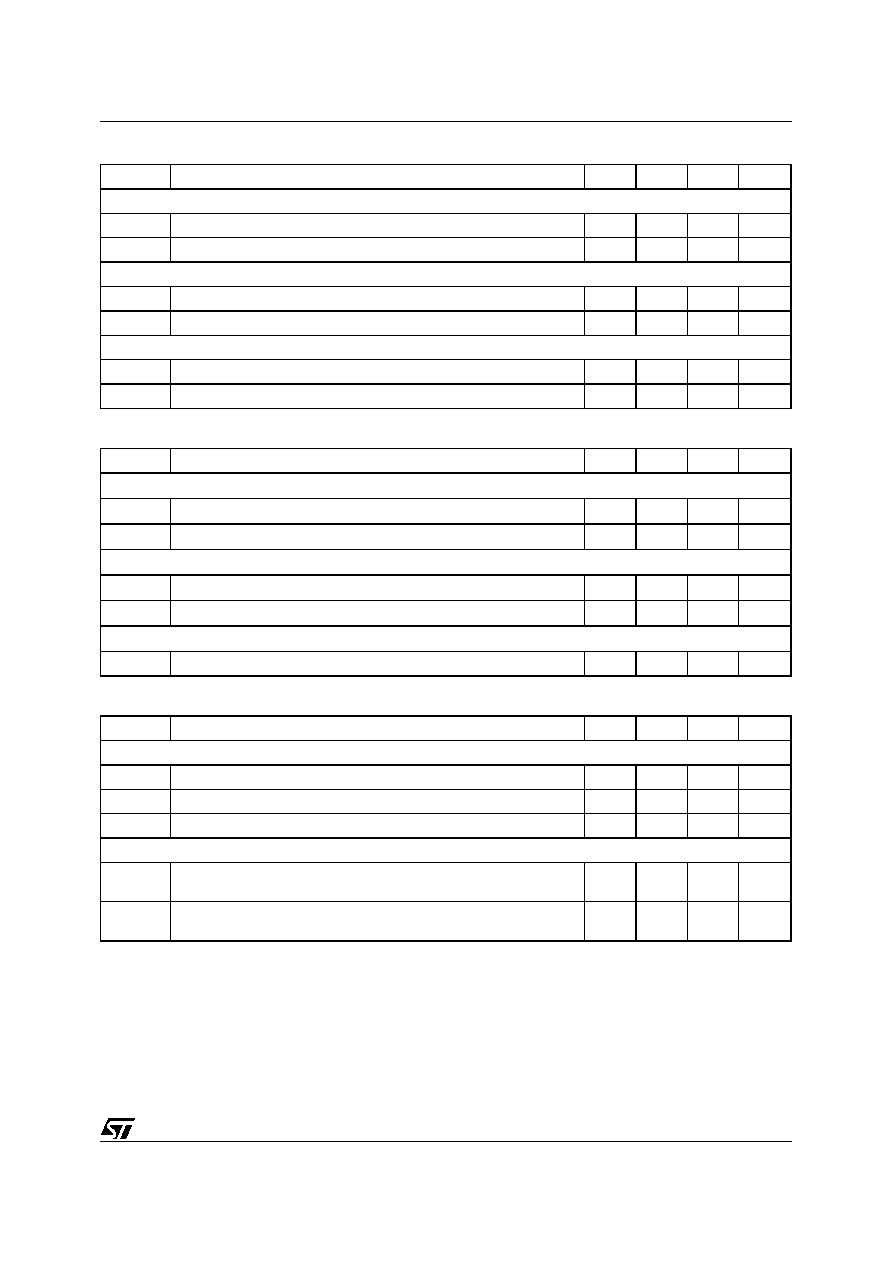
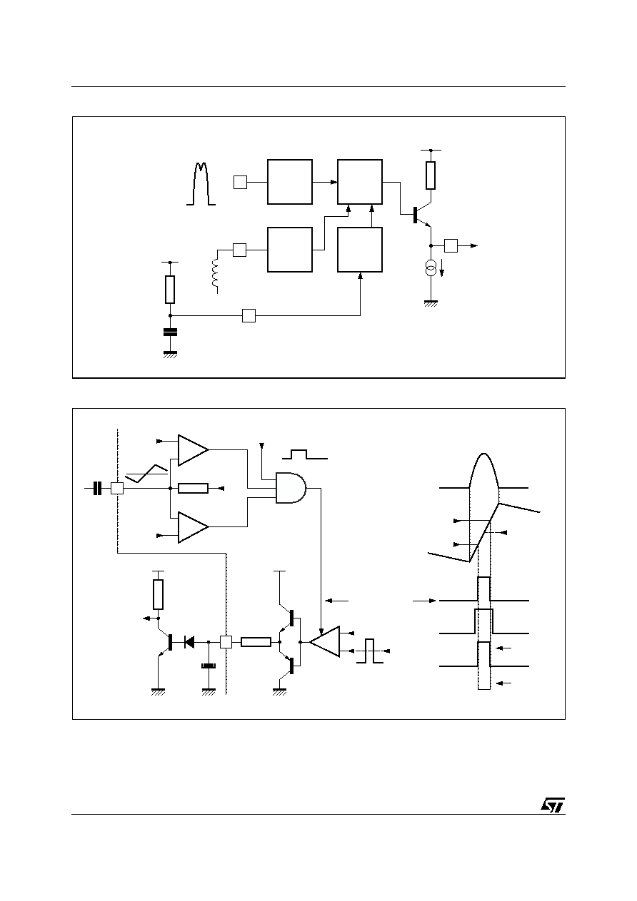
The slice level of sync-separation is fixed by value
of the external resistors R1 and R2. VR is an inter-
nally fixed voltage.
The sync-pulse allows the discharge of the capac-
itor by a 2 x I current. A line sync-pulse is not able
to discharge the capacitor under V
Z
/2. A frame
sync-pulse permits the complete discharge of the
capacitor, so during the frame sync-pulse Q
3
and
Q
4
provide current for the other parts of the circuit.
Figure 4. Synchronization Separator Circuit
Figure 5. Frame Separator
VR
R1
20
SL1
SL2
R2
Video
V
Z
V
Z/2
Q3
Q4
ST2
ST1
SL1
3l
l
TDA8215B
8/15
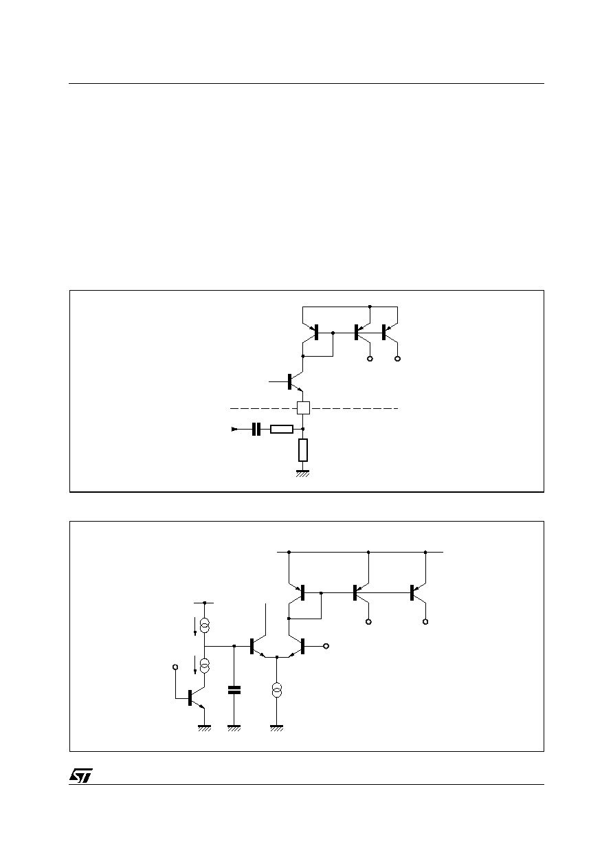
Figure 6. Line Oscillator
The oscillator thresholds are internally fixed by re-
sistors. The discharge of the capacitor depends on
the internal resistor R4. The control voltage is ap-
plied on resistor R5. The sync-pulse drives the
current in the comparator. The line flyback inte-
grated by the external net work gives on pin 13 a
saw tooth, the DC offset of this saw tooth is fixed
by VC. The comparator output provides a positive
current for the part of the signal on pin 13 greater
than to VC and a negative current for the other
part.When the line flyback and the video signal are
synchronized, the output of the comparator is an
alternatively negative and positive current. The
frame sync-pulse inhibits the comparator to pre-
vent frequency drift of the line oscillator on the
frame beginning.
Figure 7. Phase Comparator
V
CC1
11
R5
R4
Phase
comparator
output
V
C
Line
Flyback
Integrated
Flyback
Sinc pulse
Output
Current
9/15
TDA8215B
Figure 8.
Line output (Pin 17)
It is an open-collector output. The output negative
pulse time is 22µs for a 64µs period.
The oscillator thresholds are internally fixed by re-
sistors. The oscillator is synchronized during the
last half free run period. The input current during
the charge of the capacitor is less than 100nA.
Figure 9. Frame Oscillator
Frame output amplifier
This amplifier is able to drive directly the frame
yoke. Its output is short circuit and overload pro-
tected; it contains also a thermal protection.
The frame blanking is detected by the frame fly-
back generator. When the output voltage of the
frame amplifier exceeds V
CC2
-2V
BE
, the pulse is
detected. The line flyback detection is provided by
a comparator which compares the input line fly-
back pulse to an internal reference. The burst gate
pulse position is fixed by the external RC network
(Pin 14). It is referenced to the middle of the line
flyback.
This stage will detect the coincidence between the
line sync pulse (if present) and a 2µs sampling
pulse. This 2µs pulse is positioned at the center of
line sync pulse when the phase loop is locked.
This sampled detection is stored by an external
capacitor Pin 8.
The identification output level is high when video
signal is present.
Important remark: minimum saw-tooth amplitude
on Pin 13 has to be 2V
PP
(typ.: 2.5V
PP
).
V
CC1
V
C
12
ST1
SL2
13
V
CC1
To frame amplifier
Frame
sync pulse
2
INPUT CURRENT
COMPENSATION
TDA8215B
10/15
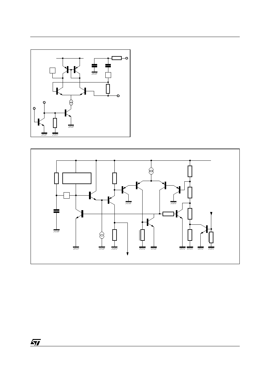
Figure 10. Super Sandcastle Generator
Figure 11. Video Identification Circuit (Pin 8)
V
CC1
V
CC1
Line
Flyback
Input
Line
Flyback
Detection
Frame
Blanking
Detection
Burst gate
pulse
generator
Frame
Output
RC
Network
RC
400µA
19
10
14
18
SSC
Output
YOKE
V
H
V
CC1
V
R1
V
R1
l8
V
CC1
V
H
V
L
V
R
2.75V
5.8
10k
1k
8
13
1N4148
Line Sync.
Sampling Pulse
Integrated
Flyback
Line
Flyback
Line
Sync.
with video
without video
BC547
V
R
2.5V
V
L
2.25V
Line retrace
Video
Ident.
Output
12µs
10µF
+
-
+
-
+
-
11/15
TDA8215B
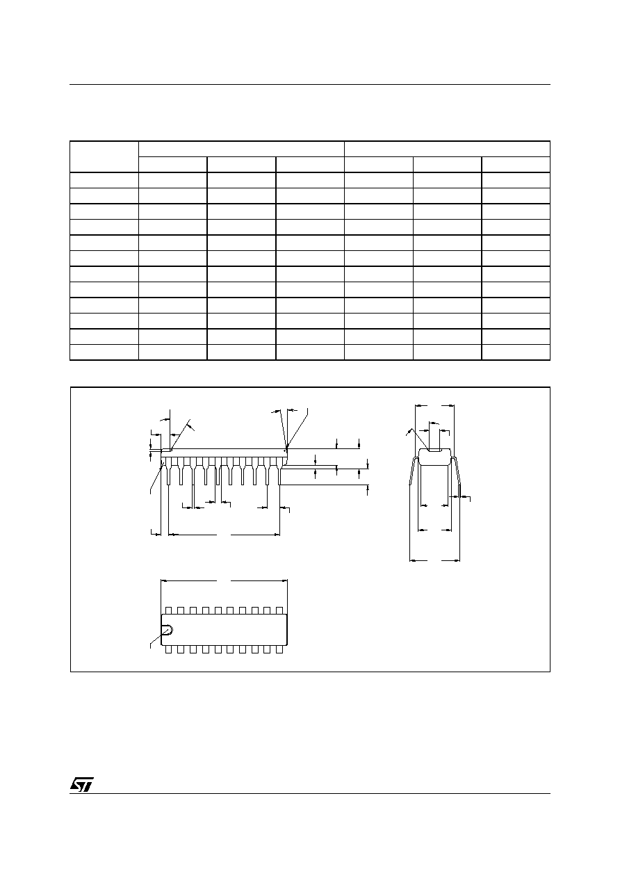
Figure 12. Typical Application
100nF
100nF
100nF
100µF
470µF
4.7k
560k
1.5k
15k
4.7k
100k
100k
1
100
100
22k
22k
22k
220k
Frame Yoke
30 mH, 15
l
pp
= 840mA
Line Yoke
193mH, 22
, ipp = 4A
Line Darlington
SGSD00055
220k
270
68pF
180pF
220pF
1000µF
680pF
22nF
2.2nF
2.2k
SSC
12nF
22nF
820k
220pF
120pF
220nF
180nF
2
1
8
3
9
4
10
7
17
19
16
15
6
5
11
12
18
13
14
20
27k
10k
2.2k
10µF
1µF
10µF
47µF
IN4148
IN4002
IN4148
Video Identification
BC547
V
CC
V
CC1
V
CC1
V
CC1
Video
Input
Line
Flyback
V
CC1
+24V
TDA 8215B
Horizontal
Frequency

TDA8215B
12/15
PART NUMBERING
Table 17. Order Codes
Part Number
Package
Temperature Range
TDA8215B
PDIP20
-0 to 70 °C
13/15
TDA8215B
PACKAGE MECHANICAL
Table 18. PLASTIC POWERDIP Mechanical Data
Figure 13. PLASTIC POWERDIP Package Dimensions
Note: Drawing is not to scale.
Symbol
millimeters
inches
Min
Typ
Max
Min
Typ
Max
a1
0.51
0.020
B
0.85
1.4
0.033
0.055
b
0.5
0.020
b1
0.38
0.5
0.015
0.020
D
24.8
0.976
E
8.8
0.346
e
2.54
0.100
e3
22.86
0.900
F
7.1
0.280
i
5.1
0.201
L
3.3
0.130
Z
1.27
0.050
K1
K2
R1
B
N
R1
A
a1
I
L
K
N
C
F
b1
E
e4
1
10
11
20
b
e3
e
N
R2
D
Z
Tie Bar Center

TDA8215B
14/15
REVISION HISTORY
Table 19. Revision History
Date
Revision
Description of Changes
September-1993
1
First Issue
17-May-2004
2
Stylesheet update. No content change.

15/15
TDA8215B
Information furnished is believed to be accurate and reliable. However, STMicroelectronics assumes no responsibility for the consequences
of use of such information nor for any infringement of patents or other rights of third parties which may result from its use. No license is granted
by implication or otherwise under any patent or patent rights of STMicroelectronics. Specifications mentioned in this publication are subject
to change without notice. This publication supersedes and replaces all information previously supplied. STMicroelectronics products are not
authorized for use as critical components in life support devices or systems without express written approval of STMicroelectronics.
The ST logo is a registered trademark of STMicroelectronics.
All other names are the property of their respective owners
© 2004 STMicroelectronics - All rights reserved
STMicroelectronics GROUP OF COMPANIES
Australia - Belgium - Brazil - Canada - China - Czech Republic - Finland - France - Germany - Hong Kong - India - Israel - Italy - Japan -
Malaysia - Malta - Morocco - Singapore - Spain - Sweden - Switzerland - United Kingdom - United States
www.st.com