 | –≠–ª–µ–∫—Ç—Ä–æ–Ω–Ω—ã–π –∫–æ–º–ø–æ–Ω–µ–Ω—Ç: TDA8218 | –°–∫–∞—á–∞—Ç—å:  PDF PDF  ZIP ZIP |
TDA8218
HORIZONTAL AND VERTICAL DEFLECTION CIRCUIT
September 1993
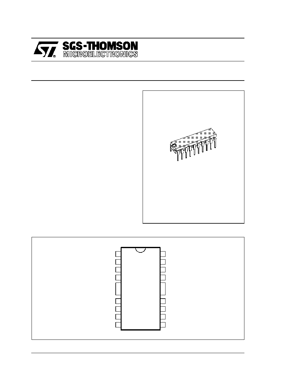
POWERDIP 16 + 2 + 2
(Plastic Package)
ORDER CODE : TDA8218
.
DIRECT FRAME-YOKE DRIVE (
±
1A)
.
COMPOSITE VIDEO SIGNAL INPUT CAPA-
BILITY
.
FRAME OUTPUT PROTECTION AGAINST
SHORT CIRCUITS
.
PLL
.
SUPER SANDCASTLE OUTPUT
.
VERY FEW EXTERNAL COMPONENTS
.
VERY LOW COST POWER PACKAGE
.
STABLE FRAME BLANKING PULSE, GEN-
ERATED BY EXTERNAL RC, FOR COMPATI-
BILITY WITH TEA 5640
1
2
3
4
5
6
7
8
9
10
20
19
18
17
16
15
14
13
12
11
FRAME OSCILLATOR
FRAME FLYBACK GENERATOR
GROUND
GROUND
POWER AMPLIFIER INPUT
FRAME POWER SUPPLY
FRAME OUTPUT
LINE OSCILLATOR
PHASE DETECTOR
LINE SAWTOOTH INPUT
GROUND
GROUND
LINE OUTPUT
LINE FLYBACK
SUPER SANDCASTLE OUTPUT
VIDEO INPUT
V
CC1
V
CC2
FRAME BLANKING R.C. NETWORK
BURST KEY R.C. NETWORK
8218-01.EPS
PIN CONNECTIONS
DESCRIPTION
The TDA8218 is an horizontal and vertical deflec-
tion circuit with super sandcastle generator. Used
with automatic PAL/SECAM decoder TEA5640,
this IC permits a complete low-cost solution for
PAL/SECAM applications.
1/9

ABSOLUTE MAXIMUM RATINGS
Symbol
Parameter
Value
Unit
V
CC
1
Supply Voltage
30
V
V
CC
2
Flyback Generator Supply Voltage
35
V
V9
Frame Power Supply Voltage
60
V
I10
NR
Frame Output Current (non repetitive)
±
1.5
A
I10
Frame Output Current (continuous)
±
1
A
V17
Line Output Voltage (external)
60
V
I
P
17
Line Output Peak Current
0.8
A
I
C
17
Line Output Continuous Current
0.4
A
T
STG
Storage Temperature
-40 to + 150
o
C
T
J
Max Operating Junction Temperature
+ 150
o
C
T
AMB
Operating Ambient Temperature
0 to 70
o
C
8218-01.TBL
THERMAL DATA
Symbol
Parameter
Value
Unit
R
TH(j-c)
Max Junction-case Thermal Resistance
10
o
C/W
R
TH(j-a)
Typical Junction-ambient Thermal Resistance
(Soldered on a 35
µ
m thick 45cm
2
PC Board copper area)
40
o
C/W
T
J
Max Recommended Junction Temperature
120
o
C
8218-02.TBL
Vcc2
Vcc1
YOKE
Vcc1
Vcc1
+
-
detector
Frame-Synchro
g enerator
Burst gate pulse
generator
Line
oscillator
Output
stage
generator
Power
s tag e
8
19
20
18
1
2
9
3
4
7
17
11
14
Video
Input
Line
Flyback
Input
stage
Frame
blanking
generator
Frame
oscillator
10
Vcc1
12
Phase
detector
13
F.B.
RC
Line flyback
Flyback
8218-02.EPS
BLOCK DIAGRAM
TDA8218
2/9

ELECTRICAL CHARACTERISTICS
V
CC1
= 10 V, T
AMB
= 25
o
C (unless otherwise specified )
Symbol
Parameter
Min.
Typ.
Max.
Unit
SUPPLY (Pin 1)
I
CC1
Supply Current
15
22
mA
V
CC1
Supply Voltage
9
10
10.5
V
VIDEO INPUT (Pin 20)
V20
Reference Voltage (I20 = -1
µ
A)
1.4
1.75
2
V
MWF
Minimum Width of Frame Pulse
(when synchronized with TTL signal)
50
µ
s
LINE OSCILLATOR (Pin 11)
LT11
Low Threshold Voltage
2.8
3.2
3.6
V
HT11
High Threshold Voltage
5.4
6.6
7.8
V
BI11
Bias Current
100
nA
DR11
Discharge Impedance
1.0
1.4
1.8
k
FLP1
Free Running Line Period
(R = 34.9k
Tied to V
CC1
, C = 2.2nF Tied to Ground)
62
64
66
µ
s
OT11
Oscillator Threshold for Line Output
Pulse Triggering
4.6
V
F
Horizontal Frequency Drift with Temperature (see application)
2
Hz/
o
C
LINE OUTPUT (Pin 17)
LV17
Saturation Voltage (I
17
= 200mA)
1.1
1.6
V
OPW
Output Pulse width (line period = 64
µ
s)
26
28
30
µ
s
LINE SAWTOOTH INPUT (Pin 13)
V13
Bias Voltage
1.8
2.4
3.2
V
Z13
Input Impedance
4.5
5.8
8
k
PHASE DETECTOR (Pin 12)
I12
Output Current During Synchro Pulse
250
350
500
µ
A
RI12
Current Ratio (positive/negative)
0.95
1
1.05
LI12
Leakage Current
-2
+2
µ
A
CV12
Control RangeVoltage
2.60
7.10
V
FRAME BLANKING GENERATOR (Pin 8)
External R.C. Network (Typical values : R = 100k
, C = 22nF)
T
fb
Blanking Time (PIn 19, T
fb
= K8 .R.C.)
1.35
ms
K8
Time Blanking Coefficient
0.588
0.613
0.644
I
O8
Output Current during the Frame Blanking : V
8
= 2V
- 0.2
1
µ
A
I
I8
Input Current after the Frame Blanking : V
8
= 7V
300
450
600
µ
A
FRAME OSCILLATOR (Pin 2)
LT2
Low Threshold Voltage
1.6
2.0
2.3
V
HT2
High Threshold Voltage
2.6
3.1
3.6
V
DIF2
LT2 - HT2
1.0
V
BI2
Bias Current
30
nA
DR2
Discharge Impedance
300
470
700
FFP1
Free Running Frame Period
(R = 866k
Tied to V
CC
1, C = 220nF Tied to Ground)
20.5
23
25
ms
MFP
Minimum Frame Period (I20 = -100
µ
A) with the Same RC
12.8
ms
FPR
Frame Period Ratio = FFP/MFP
1.7
1.8
1.9
8218-03.TBL
TDA8218
3/9

ELECTRICAL CHARACTERISTICS
V
CC1
= 10 V, T
AMB
= 25
o
C (unless otherwise specified )
Symbol
Parameter
Min.
Typ.
Max.
Unit
FRAME OSCILLATOR (Pin 2) (continued)
FG
Frame Saw-tooth Gain Between Pin 1 and non Inverting Input of the
Frame Amplifier
-0.4
F
Vertical Frequency Drift with Temperature (see application)
4.10
-3
Hz/
o
C
FRAME POWER SUPPLY (Pin 9)
V9
Operating Voltage (with flyback Generator)
10
58
V
I9
Supply Current (V9 = 30V)
9
15
mA
FLYBACK GENERATOR SUPPLY (Pin 3)
V
CC
2
Operating Voltage
10
30
V
FRAME OUTPUT (Pin 10)
Saturation Voltage to Ground (V9 = 30V)
LV10A
I10 = 0.1A
0.06
0.6
V
LV10B
I10 = 1A
0.37
1
V
Saturation Voltage to V9 (V9 = 30V)
HV10A
I10 = -0.1A
1.3
1.6
V
HV10B
I10 = -1A
1.7
2.4
V
Saturation Voltage to V9 in Flyback Mode (V10 > V9)
FV10A
I10 = 0.1A
1.6
2.1
V
FV10B
I10 = 1A
2.5
4.5
V
FLYBACK GENERATOR (Pin 3 and Pin 4)
Flyback Transistor on (output = high state), V
CC2
= 30V, V4/3 with
F2DA
F2DB
I
4
3
= 0.1A
I
4
3
= 1A
1.5
3.0
2.1
4.5
V
V
Flyback Transistor on (output = high state), V
CC2
= 30V, V3/4 with
FSVA
FSVB
I
3
4
= 0.1A
I
3
4
= 1A
0.8
2.2
1.1
4.5
V
V
Flyback Transistor off (output = V9 - 8V), V9 - V
CC2
= 30V
FCI
Leakage Current Pin 3
170
µ
A
SUPER SANDCASTLE OUTPUT (Pin 19)
Output Voltages (R load = 2.2k
)
SANDT2
Frame blanking pulse level
2
2.5
3
V
SANDL2
Line blanking pulse level
4
4.5
5
V
BG2
Burst key pulse level
8
9
V
Pulses width and timing
SC3
Delay between middle of sync pulse and leading edge of burst key pulse
2.3
2.7
3.1
µ
s
SC2
Duration of burst key pulse
Vertical blanking pulse width : Defined by external R.C. Pin 8
3.7
4
5
µ
s
LINE FLYBACK INPUT (Pin 18)
Switching level
2
V
Maximum imput current at V
PEAK
= 800V
8
mA
Limiting voltage at maximum current
4.3
V
RC network time constant (Note 1) for the burst key pulse
6
µ
S
Note :
1. An RC network is connected to this input. Typical value for the resistor is 27k
and 220pF for the capacitor. A different time
constant for RC changes the delay between the middle of the line synchro pulse and the leading edge of the burst key pulse
but also the duration of the burst key pulse.
8218-04.TBL
TDA8218
4/9

The TDA8218 performs all the video and power
functions required to provide signals for the line
driver and frame yoke.
It contains:
∑
A synchronization separator
∑
An integrated frame separator without external
components
∑
A saw-tooth generator for the frame
∑
A power amplifier for direct drive of frame yoke
(short circuit protected)
∑
An open collector output for the line driver
∑
A line phase detector and a voltage control os-
cillator
∑
A super sandcastle generator.
GENERAL DESCRIPTION
20
SL2
SL1
VR
Video
R1
R2
8218-03.EPS
Figure 1 : Synchronization Separator Circuit
Vz
ST2
ST1
I
3I
SL1
Vz
/2
Q3
Q4
8218-04.EPS
Figure 2 : Frame Separator
The slice level of sync-separation is fixed by value of the external resistors R1 and R2. V
R
is an internally
fixed voltage.
The sync-pulse allows the discharge of the capaci-
tor by a 2 x I current. A line sync-pulse is not able
to discharge the capacitor under V
Z
/2. A frame
sync-pulse permits the complete discharge of the
capacitor, so during the frame sync-pulse Q
3
and
Q
4
provide current for the other parts of the circuit.
TDA8218
5/9