 | –≠–ª–µ–∫—Ç—Ä–æ–Ω–Ω—ã–π –∫–æ–º–ø–æ–Ω–µ–Ω—Ç: TDA9203A | –°–∫–∞—á–∞—Ç—å:  PDF PDF  ZIP ZIP |
TDA9203A
I
2
C BUS CONTROLLED 70MHz RGB PREAMPLIFIER
June 1998
SHRINK 24
(Plastic Package)
ORDER CODE : TDA9203A
.
70MHz TYPICAL BANDWIDTH AT 4V
PP
OUT-
PUT WITH 12pF CAPACITIVE LOAD
.
5.5ns TYPICAL RISE/FALL TIME AT 4V
PP
OUTPUT WITH 12pF CAPACITIVE LOAD
.
POWERFULL OUTPUT DRIVE CAPABILITY
.
BRT, CONT, DRIVE, OUTPUT DC LEVEL,
OSD CONTRAST, BACK-PORCH CLAMPING
PULSE WIDTH ARE I
2
C BUS CONTROLLED
.
INTERNAL
BACK-PORCH
CLAMPING
PULSE GENERATOR
.
OSD WHITE BALANCE TRACKING
.
INTERNAL OSD SWITCHES
.
BLANKING AND FAST-BLANKING INPUTS
.
VERY LARGE DRIVE ADJUSTMENT RANGE
(48dB)
.
SEMI-TRANSPARENT BACKGROUND ON
OSD PICTURE
.
ABL CONTROL
DESCRIPTION
The TDA9203A is a digitaly controlled wideband
video preamplifier intended for use in mid range
color monitor. All controls and adjustments are
digitaly performed thanks to I
2
C serial bus. Con-
trast, brightness and DC output level of RGB sig-
nals are common to the 3 channels and drive
adjustment is separate for each channel. Three I
2
C
gain controlled OSD inputs can be switched with
RGB signals using fast blanking command. Clamp-
ing of RGB signals is performed thanks to a flexible
integrated system. The white balance adjustment
is effective on brightness, video and OSD signals.
The TDA9203A works for application using AC or
DC coupled CRT driver.
The ABL input provides a 12dB Max. attenuation
on the current contrast value according average
beam limitation voltage.
Because of its features and due to component
saving the TDA9203A leads to a very performant
and cost effective application.
1
2
3
4
5
6
7
8
9
10
20
19
18
17
16
15
14
13
24
23
22
21
11
12
HSYNC
PV
CC1
OUT1
PGND1
PV
CC2
OUT2
PGND2
PV
CC3
OUT3
PGND3
BLK
FBLK
IN1
OSD1
AV
DD
IN2
OSD2
AGND
IN3
OSD3
ABL
LGND
SDA
SCL
920
3A
-
01.
E
P
S
PIN CONNECTIONS
1/13

Name
Pin
Type
Fun ction
IN1
1
I
1
st
Channel Main Picture Input
OSD1
2
I
1
st
Channel OSD Input
AV
DD
3
I
12V Analog V
DD
IN2
4
I
2
nd
Channel Main Picture Input
OSD2
5
I
2
nd
Channel OSD Input
AGND
6
I/O
Analog Ground
IN3
7
I
3
rd
Channel Main Picture Input
OSD3
8
I
3
rd
Channel OSD Input
ABL
9
I
ABL Input
LGND
10
I/O
Logic Ground
SDA
11
I/O
Serial Data Line
SCL
12
I
Serial Clock Line
Name
Pin
Type
Function
FBLK
13
I
Fast Blanking Input
BLK
14
I
Blanking Input
PGND3
15
I/O
3
rd
Channel Power Ground
OUT3
16
O
3
rd
Channel Output
PV
CC3
17
I
3
rd
Channel Power V
CC
PGND2
18
I/O
2
nd
Channel Power Ground
OUT2
19
O
2
nd
Channel Output
PV
CC2
20
I
2
nd
Channel Power V
CC
PGND1
21
I/O
1
st
Channel Power Ground
OUT1
22
O
1
st
Channel Output
PV
CC1
23
I
1
st
Channel Power V
CC
HSYNC
24
I
Horizontal Synch Input
9203A
-
0
1
.
T
B
L
PIN DESCRIPTION
1
2
3
4
5
6
7
8
9
10
11
12
13
14
15
16
17
18
19
20
21
22
23
24
CLAMP
V
REF
AV
DD
IN1
AGND
IN2
BRIGHTNESS
IN3
OUTPUT
STAGE
DRIVE
8 bits
BPCP
PV
CC1
FBLK
BLK
OUT1
PGND1
PV
CC2
OUT2
PGND2
OUT3
PGND3
PV
CC3
ABL
LGND
I
2
C
BUS
DECODER
D/A
LATCHES
BPCP
SCL
SDA
HSYNC
OSD
OSD1
OSD2
OSD3
GREEN CHANNEL
BLUE CHANNEL
I
2
C
V
REF
OUTPUT
DC LEVEL
ADJUST
TDA9203A
CONTRAST
CONT
92
03A
-
0
2.
E
P
S
BLOCK DIAGRAM
TDA9203A
2/13
BLK
HSYNC
BPCP
Internal pulse width is controlled by I
2
C
92
03A
-
0
3.
E
P
S
Figure 1
FUNCTIONAL DESCRIPTION
Input Stage
The R, G and B signals must be fed to the three
inputs through coupling capacitors (100nF).
The maximum input peak-to-peak video amplitude
is 1V.
The input stage includes a clamping function. This
clamp is using the input serial capacitor as "mem-
ory capacitor" and is gated by an internally gener-
ated "Back-Porch-Clamping-Pulse (BPCP)".
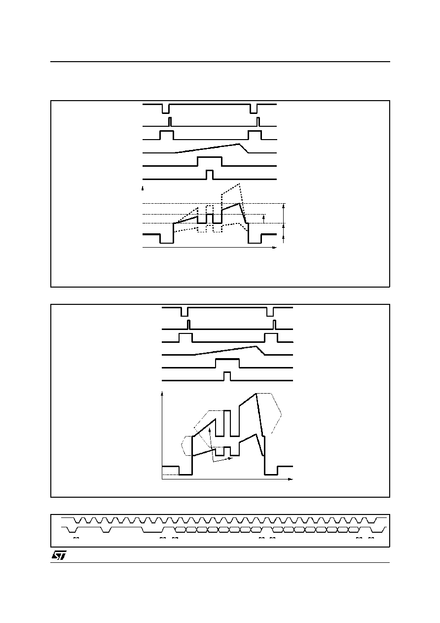
The synchronization edge of the BPCP is selected
according bit 0 of register R8.
When B0R8 is set to 1, the BPCP is synchronized
on the leading edge of the blankingpulse BLKinputs
on Pin14 (seeFigure1). B7R8 allows to use positive
or negative blanking signal on Pin 14. At power on
reset TDA9203A use only positive blanking.
When B0R8 is clear to 0, the BPCP is synchronized
on the second edge of the horizontal pulse HSYNC
inputs on Pin 24. An automatic function allows to
use positive or negative horizontal pulse on Pin 24
(see Figure 2).
In both case BPCP width is adjustable by I
2
C, B1
and B2 of register R8 (see R8 Table P8).
Contrast Adjustment (8 bits)
The contrast adjustment is made by controlling
simultaneously the gain of three internal variable
gain amplifiers through the I
2
C bus interface.
The contrast adjustment allows to cover a typical
range of 48dB.
ABL Control
The TDA9203A I
2
C preamplifier provides an ABL
input (automatic beam limitation) to attenuat e
R,G,B video signals according to beam intensity.
The operating range is 2.5V typicaly, from 5.3V to
2.8V. A typical 12dB Max. attenuation is applied to
the signal whatever the current gain is. Refer to
Figure 3 for ABL input attenuation range.
In case of software control, the ABL input must be
pulled to AV
DD
through a resistor to limit power
consumption (see Figure 11).
ABL input voltage must not exceeed AV
DD
. Input
resistor is 10k
and equivalent schematic given in
Figure 11.
HSYNC
BPCP
Internal pulse width is controlled by I
2
C
920
3A
-
04.
E
P
S
Figure 2
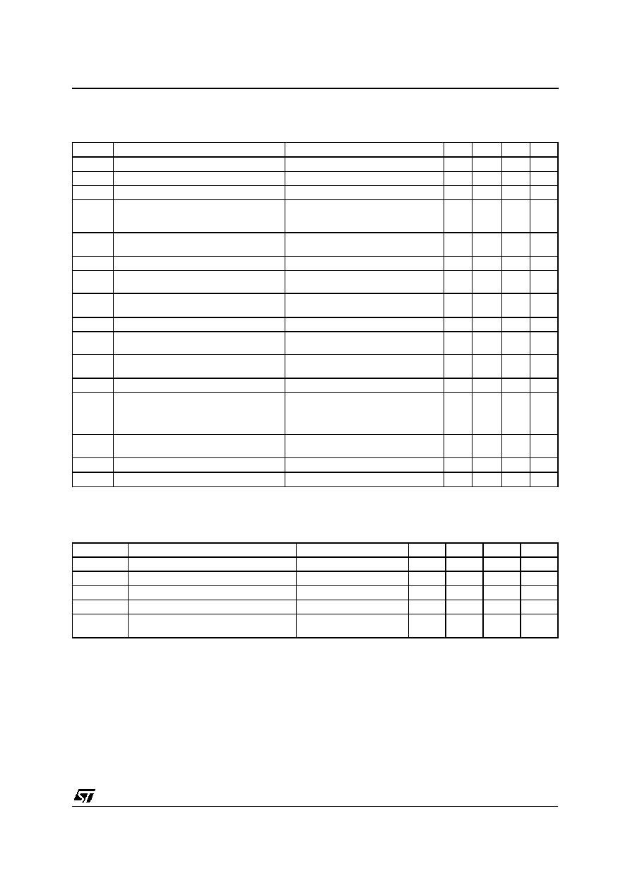
Brightness Adjustment (8 bits)
As for the contrast adjustment, the brightness is
controlled by I
2
C.
The brightness function consists to add the same
DC offset to the three R, G, B signals after contrast
amplification. This DC-Offset is present only out-
side the blanking pulse (see Figure 4).
The DC output level during the blanking pulse, is
forced to "INFRA-BLACK" level (V
DC
).
Drive Adjustment (3 x 8 bits)
In order to adjust the white balance , the TDA9203A
offers the possibility to adjust separately the overall
gain of each complete video channel. The gain of
each channel is controlled by I
2
C (8bits each).
The very large drive adjustment range (48dB) allows
different standard or custom color temperature.
It can also be used to adjust the output voltages at
the optimum amplitude to drive the C.R.T drivers,
keepingthe whole contrast control for end-useronly.
The drive adjustment is located after the CON-
TRAST, BRIGHTNESS and OSD switch blocks, so
that the white balance will remains correct when
BRT is adjusted, and will also be correct on OSD
portion of the signal.
2
0
-2
-4
-6
-8
-10
-12
-14
1
2
3
4
5
6
7
8
9
Attenuation (dB)
V
IN
(V)
9203
A
-
0
X
.
E
P
S
Figure 3
TDA9203A
3/13

FUNCTIONAL DESCRIPTION (continued)
OSD Inputs
The TDA9203A includes all the circuitry necessary
to mix OSDsignals into the RGB main-picture. Four
pins are dedicated to this function as follow.
Three TTL RGB On Screen Display inputs (Pin 2,
5 and 8). These three inputs are connected to the
three outputs of the corresponding ON-SCREEN-
DISPLAY processor (ex : STV942x).
One Fast Blanking Input (FBLK, Pin 13) which is
also connected to the FBLK output of the same
ON-SCREEN-DISPLAY processor.
When a high level is present on FBLK, the IC will
acts as follow :
- The three main picture RGB input signals are
internally switched to the internal input clamp
reference voltage.
- The three output signals are set to voltages cor-
respondingto the state (0 or 1) on the three OSD
inputs (see Figure 4).
Example :
If FBLK = 1 and OSD1, OSD2, OSD3) = 1, 0, 1
respectively.
Then OUT1, OUT2, OUT3 will be equal to V
OSD
,
V
BRT
, V
OSD
,
where : V
BRT
= V
BLACK
+ BRT, V
OSD
= V
BRT
+ OSD
BRT is the brightness DC level I
2
C adjustable.
OSD is the On-Screen Display signal value I
2
C
adjustable from 0V to 5.5V
PP
by step of 0.36V.
Semi-transparent function is controlled thanks to
Bit 6 of R8 register (see Table 1).
When semi-transparent mode is activated, video
signal is divided by 2 (CONT).
Table 1
FBLK OSD1 OSD2 OSD3 B6R8
Output
Signal (OUTn)
0
x
x
x
0
Video
1
x
x
x
0
OSD (1)
0
x
x
x
1
Video
1
0
x
x
1
OSD
1
x
1
x
1
OSD
1
x
x
0
1
OSD
1
1
0
1
1
Semi-trans-
parent (2)
Notes : 1. All OSD colors are displayed.
2. One OSD color is displayed as semi-transparent video
without effect on brightness and DC level adjustment.
Output Stage
The three output stagesincorporate threefunctions
which are :
- The blanking stage : When high level is applied
to the BLK input (Pin 14), the three outputs are
switched to a voltage which is 400mV lower than
the BLACK level. The black level is the output
voltage with minimum brightness when input sig-
nal video amplitude is equal to "0".
- The output stage itself : It is a large bandwidth
output amplifier which allow to deliver up to 5V
PP
on the three outputs (for 0.7V video signal on the
inputs).
- The output CLAMP : The IC also incorporates
three internal output clamp (sample and hold
system) which allow to DC shift the three output
signals. The DC output voltage is adjustable
through I
2
C with 4 bits. Practicaly, the DC output
level allow to adjust the BLK level (V
DC
= 400mV
under V
BLACK
) from 0.9V to 2.9V with 12 x 165mV.
The overall waveforms of the output signal accord-
ing to the different adjustment are shown in Fig-
ures 4 and 5.
Serial Interface
The 2-wires serial interface is an I
2
C interface.
The slave address of the TDA9203A is DC (in
hexadecimal).
A6
A5
A4
A3
A2
A1
A0
W
1
1
0
1
1
1
0
0
Data Transfer
The host MCU can write data into the TDA9203A
registers. Read mode is not available.
To write data into the TDA9203A, after a start, the
MCU must send (see Figure 6) :
- The I
2
C addressslave byte with a low level for the
R/W bit.
- The byte of the internal register address where
the MCU wants to write data(s).
- The data.
All bytes are sent MSB bit first and the write data
transter is closed by a stop.
TDA9203A
4/13
HSYNC
V
CONT
(4)
BPCP
BLK
Video IN
FBLK
OSD IN
V
OSD
(5)
V
BRT
(3)
V
BLACK
(2)
V
DC
(1)
CONT
OSD
BRT
0.4V fixed
V
OUT1
, V
OUT2
, V
OUT3
Notes : 1.
V
DC
= 0.5 to 2.5V
2.
V
BLACK
= V
DC
+ 0.4V
3.
V
BRT
= V
BLACK
+ BRT (with BRT = 0 to 2.5V)
4.
V
CONT
= V
BRT
+ CONT with CONT = k x Video IN (CONT = 5V
P P
max. for V
IN
= 0.7V
PP
)
5.
V
OSD
= V
BRT
+ OSD with OSD = k1 x OSDIN (OSD max. = 5.5V
PP
, OSD min. = 360mV
PP
)
9203
A
-
0
6
.
E
P
S
Figure 4 : Waveforms VOUT, BRT, CONT, OSD
HSYNC
V
CONT
BPCP
BLK
Video IN
FBLK
OSD IN
V
OSD
V
BRT
V
BLACK
V
DC
V
OUT1
, V
OUT2
, V
OUT3
Note : 1. Drive adjustment modifies the following voltages : V
CONT
, V
BRT
and V
OSD
.
Drive adjustment do not modify the following voltages : V
DC
and V
BLACK
.
Two exemples
of drive adjustment
(1)
9203
A
-
0
7
.
E
P
S
Figure 5 : Waveforms (DRIVE adjustment)
FUNCTIONAL DESCRIPTION (continued)
SCL
W
A7
A6
A5
A4
A3
A2
A1
A0
SDA
Register Address
ACK
ACK
I
2
C Slave Address
Start
D7
D6
D5
D4
D3
D2
D1
D0
Data Byte
ACK
Stop
9203A
-
0
8
.
E
P
S
Figure 6 : I
2
C Write Operation
TDA9203A
5/13

QUICK REFERENCE DATA
Symbol
Parameter
Min.
Typ.
Max.
Unit
Signal Bandwidth (4V
PP
/12pF load)
70
MHz
Rise and Fall Time (4V
PP
/12pF load)
5.5
ns
Drive Adjustment Range on the 3 Channels separately
48
dB
Maximum Output Voltage (V
IN
= 0.7 V
PP
)
5
V
PP
Output Voltage Range (AC + DC)
8
V
9
203
A
-
02.
T
B
L
ABSOLUTE MAXIMUM RATINGS
Symbol
Parameter
Value
Unit
V
S
Supply Voltage (Pins 3-9-17-20-23)
14
V
V
IN1
Voltage at any Input Pins (except SDA & SCL & Logical Inputs)
GND < V
IN1
< V
S
V
V
IN2
Voltage at Input Pins SDA & SCL
GND < V
IN2
< 5.5
V
V
IN3
Voltage at Logical Inputs (OSD, FBLK, BLK, HSYNC)
GND < V
IN3
< 5.5
V
V
ESD
ESD Susceptability (Human body model ; 100pF Discharge through 1.5k
)
2
kV
T
stg
Storage Temperature
- 40, + 150
∞
C
T
j
Junction Temperature
150
∞
C
T
op er
Operating Temperature
0, + 70
∞
C
920
3A
-
03.
T
B
L
THERMAL DATA
Symbol
Parameter
Value
Unit
R
th (j-a)
Junction-ambient Thermal Resistance
69
o
C/W
92
03
A
-
04.
T
B
L
DC ELECTRICAL CHARACTERISTICS (T
amb
= 25
o
C, V
CC
= 12V, unless otherwise specified)
Symbol
Parameter
Test Conditions
Min.
Typ.
Max.
Unit
V
S
Supply Voltage
Pins 3-9-17-20-23
10.8
12
13.2
V
I
S
Supply Current (All V
S
Pin current)
R
L
= 1k
60
mA
V
I
Video Input Voltage Amplitude
Pins 1-4-7
0.7
1
V
PP
V
O
Typical Output Voltage Range
Pins 16-19-22
0.5
-
8
V
V
IL
Low Level Input (OSD, FBLK, BLK, HSYNC)
Pins 2-5-8-13-14-24
0.8
V
V
IH
High Level Input (OSD, FBLK, BLK, HSYNC)
Pins 2-5-8-13-14-24
2.4
V
I
IN
Input Current (OSD, FBLK, BLK, HSYNC)
0.4V < V
IN
< 4.5V
-10
+10
µ
A
92
03
A
-
0
5
.
T
B
L
TDA9203A
6/13
AC ELECTRICAL CHARACTERISTICS
(T
amb
= 25
o
C, V
CC
= 12V, C
L
= 12pF, R
L
= 1k
, unless otherwise specified)
Symbol
Parameter
Test Conditions
Min.
Typ.
Max.
Unit
AV
Maximum Gain (20 log x V
OUT AC
/V
IN AC
)
Contrast & Drive at maximum
18
dB
CAR
Contrast Attenuation Range
V
IN
= 0.7V
PP
, Contrast & Drive at POR
48
dB
DAR
Drive Attenuation Range
48
dB
GM
Gain Match
V
OUT
= 2.5V
PP
, V
IN
= 0.7V
PP
Contrast = Drive = Maxi x 0.7
(power-on reset value)
±
0.1
dB
BW
Bandwidth Large Signal
At -3dB, V
IN
= 0.7V
PP
, V
OUT
= 4V
PP
Contrast = Drive = Maxi x 0.87
70
MHz
DIS
Video Output Distorsion (see Note)
f = 1MHz, V
OUT
= 1V
PP
, V
IN
= 1V
PP
0.3
%
t
R
, t
F
Video Output Rise and Fall Time
(see Note)
VIN = 0.7V
PP
, V
OUT
= 4V
PP
Contrast = Drive = Maxi x 0.87
5.5
ns
BRT
Brightness Maximum DC Level
Brightness Minimum DC Level
2.5
0
V
V
BRTM
Brightness Matching
BRT = 50%, Drive at POR
±
20
mV
OSD
CAR
Contrast Attenuation Range
for OSD Input
24
dB
DC
Output Maximum DC Level
Output Minimum DC Level
2.5
0.5
V
V
R
L
Equivalent Load on Video Output
with T
j
T
j Max.
1
k
CT
Croostalk between Video Channels
(see Note)
V
OUT
= 2.5V
PP
, V
IN
= 0.7V
PP
Contrast = Drive = Maxi x 0.7
(power-on reset value)
f
IN
= 1MHz
44
dB
G
ABL
ABL Min. Attenuation
ABL Max. Attenuation
V
ABL
= 5.3V Typical
V
ABL
= 2.8V Typical
0
12
dB
dB
I
ABL
ABL Input Current
V
ABL
= 5.3V
20
µ
A
R
ABL
ABL Input Resistor
See Figure 11
10
k
Note :
These parameters are not tested on each unit. They are measured during an internal qualification procedure which includes
characterization on batches coming from corners of our processes and also from temperature characterization.
92
03
A
-
06.
T
B
L
I
2
C ELECTRICAL CHARACTERISTICS (T
amb
= 25
o
C, V
CC
= 12V, unless otherwise specified)
Symbol
Parameter
Test Conditions
Min.
Typ.
Max.
Unit
V
IL
Low Level Input Voltage
On Pins SDA, SCL
1.5
V
V
IH
High Level Input Voltage
3
V
I
IN
Input Current (Pins SDA, SCL)
0.4V < V
IN
< 4.5V
-10
+10
µ
A
f
SCL(Max.)
SCL Maximum Clock Frequency
200
kHz
V
OL
Low Level Output Voltage
SDA Pin when ACK
Sink Current = 6mA
0.6
V
92
03
A
-
08.
T
B
L
TDA9203A
7/13

t
HDAT
t
SUDAT
t
LOW
t
HIGH
t
HDS
t
SUP
t
BUF
SDA
SCL
9203
A
-
0
9
.
E
P
S
Figure 7
I
2
C INTERFACE TIMINGS REQUIREMENTS (see Figure 7)
Symbol
Parameter
Min.
Typ.
Max.
Unit
t
BUF
Time the bus must be free between 2 access
1300
ns
t
HDS
Hold Time for Start Condition
600
ns
t
SUP
Set-up Time for Stop Condition
600
ns
t
LOW
The Low Period of Clock
1300
ns
t
HIGH
The High Period of Clock
600
ns
t
HDAT
Hold Time Data
300
ns
t
SUDAT
Set-up Time Data
250
ns
t
R
, t
F
Rise and Fall Time of both SDA and SCL
20
300
ns
92
03
A
-
0
9
.
T
B
L
TDA9203A
8/13
REGISTER DESCRIPTION
Registers Sub-address
Address (Hex)
Register Names
Function
POR Value
01
Contrast
DAC 8-bit
B4
02
Brightness
DAC 8-bit
B4
03
Drive 1
DAC 8-bit
B4
04
Drive 2
DAC 8-bit
B4
05
Drive 3
DAC 8-bit
B4
06
Output DC Level
DAC 4-bit
08
07
OSD Contrast
DAC 4-bit
08
08
BP and Miscellaneous
See R8 Table
04
Contrast Register (R1) (Video IN = 0.5V
PP
, Brightness at minimum,Drive at maximum)
Hex
b7
b6
b5
b4
b3
b2
b1
b0
CONT (V
PP
)
G (dB)
POR Value
00
0
0
0
0
0
0
0
0
0
-
01
0
0
0
0
0
0
0
1
0.015
-30
02
0
0
0
0
0
0
1
0
0.031
-24
04
0
0
0
0
0
1
0
0
0.062
-18
08
0
0
0
0
1
0
0
0
0.125
-12
10
0
0
0
1
0
0
0
0
0.25
-6
20
0
0
1
0
0
0
0
0
0.5
0
40
0
1
0
0
0
0
0
0
1
6
80
1
0
0
0
0
0
0
0
2
12
B4
1
0
1
1
0
1
0
0
2.812
15
X
FF
1
1
1
1
1
1
1
1
4
18
Brightness Register (R2) (Drive at maximum)
Hex
b7
b6
b5
b4
b3
b2
b1
b0
BRT (V)
POR Value
00
0
0
0
0
0
0
0
0
0
01
0
0
0
0
0
0
0
1
0.010
02
0
0
0
0
0
0
1
0
0.020
04
0
0
0
0
0
1
0
0
0.040
08
0
0
0
0
1
0
0
0
0.080
10
0
0
0
1
0
0
0
0
0.160
20
0
0
1
0
0
0
0
0
0.320
40
0
1
0
0
0
0
0
0
0.640
80
1
0
0
0
0
0
0
0
1.28
B4
1
0
1
1
0
1
0
0
1.8
X
FF
1
1
1
1
1
1
1
1
2.56
TDA9203A
9/13
REGISTER DESCRIPTION (continued)
Drive Registers (R3, R4, R5) (Video IN = 0.5V
PP
, Brightness at minimum, Contrast at maximum)
Hex
b7
b6
b5
b4
b3
b2
b1
b0
CONT (V
PP
)
G (dB)
POR Value
00
0
0
0
0
0
0
0
0
0
-
01
0
0
0
0
0
0
0
1
0.015
-30
02
0
0
0
0
0
0
1
0
0.031
-24
04
0
0
0
0
0
1
0
0
0.062
-18
08
0
0
0
0
1
0
0
0
0.125
-12
10
0
0
0
1
0
0
0
0
0.25
-6
20
0
0
1
0
0
0
0
0
0.5
0
40
0
1
0
0
0
0
0
0
1
6
80
1
0
0
0
0
0
0
0
2
12
B4
1
0
1
1
0
1
0
0
2.812
15
X
FF
1
1
1
1
1
1
1
1
4
18
Output DC Level Register (R6)
Hex
b7
b6
b5
b4
b3
b2
b1
b0
DC (V)
POR Value
03
0
0
0
0
0
0
1
1
0.52
04
0
0
0
0
0
1
0
0
0.69
08
0
0
0
0
1
0
0
0
1.35
X
0F
0
0
0
0
1
1
1
1
2.5
Code 00Hex, 01Hex and 02Hex : not to be used
OSD Contrast Register (R7) (V
OSD IN
= 2.4V
Min
.., Drive at maximum)
Hex
b7
b6
b5
b4
b3
b2
b1
b0
OSD (V)
G (dB)
POR Value
00
0
0
0
0
0
0
0
0
0
-
01
0
0
0
0
0
0
0
1
0.36
-24
02
0
0
0
0
0
0
1
0
0.73
-18
04
0
0
0
0
0
1
0
0
1.46
-12
08
0
0
0
0
1
0
0
0
2.93
-6
X
0F
0
0
0
0
1
1
1
1
5.5
0
BP and Miscellaneous Register (R8)
b7
b6
b5
b4
b3
b2
b1
b0
Function
POR Value
0
BP Source = HSYNC
X
1
BP Source = BLK
0
0
BP Pulse Width = 0.33
µ
s
0
1
BP Pulse Width = 0.66
µ
s
1
0
BP Pulse Width = 1
µ
s
X
1
1
BP Pulse Width = 1.3
µ
s
0
0
Test Purposes
X
0
0
0
Soft Blanking OFF
X
1
1
1
Soft Blanking ON
0
Semi Transparent OFF
X
1
Semi Transparent ON
0
Positive Blanking Polarity Selection
X
1
Negative Blanking Polarity Selection
TDA9203A
10/13

INTERNAL SCHEMATICS
AGND
AGND
AV
DD
IN
P ins
1-4-7
920
3A
-
10.
E
P
S
Figure 8
AGND
AGND
AV
DD
OS D - BLK - FBLK
P ins 2-5-8-13-14
92
03A
-
1
1.
E
P
S
Figure 9
3
6
AV
DD
AGN D
(20V)
9
203A
-
1
2
.
E
P
S
Figure 10
9
ABL
10k
AV
DD
Internal
5V
AGND
9
203A
-
1
3
.
E
P
S
Figure 11
10
LGND
AV
DD
AGND
LGND
92
03A
-
1
4.
E
P
S
Figure 12
S DA
S CL
P ins
11-12
(10V)
AGND
LGND
9
203A
-
1
5
.
E
P
S
Figure 13
24
AGND
LGND
AV
DD
HSYNC
9203A
-
1
6
.
E
P
S
Figure 14
P ins 17-20-23
P ins 15-18-21
Pins 16-19-22
OUT
PV
C C
P GND
AGND
AV
DD
92
03
A
-
17.
E
P
S
Figure 15
TDA9203A
11/13

1
2
3
4
5
6
7
8
9
10
16
17
18
19
20
11
12
13
14
15
21
22
23
24
IN1
OSD1
AV
DD
IN2
OSD2
AGND
IN3
OSD3
SCL
SDA
LGND
HSYNC
PV
CC1
OUT1
PGND1
PV
CC2
OUT2
PGND2
PV
CC3
PGND3
OUT3
BLK
FBLK
T
D
A
9
2
0
3
A
+12V
1k
GND
GND
BLUE OUT
RED OUT
GREEN OUT
1k
1k
1k
100nF
100nF
100nF
100nF
100nF
47
47
47
75
75
75
B
GND B
R
GND R
G
GND G
100nF
100nF
100nF
1
2
3
4
5
6
7
8
16
13
14
15
12
11
10
9
FBLK
VSYNC
HSYNC
V
DD
PXCK
CKOUT
XTAL OUT
XTAL IN
TEST
B
G
R
RESET
SDA
SCL
S
T
V
9
4
2
6
GND
+5V
100nF
+5V
8MHz
33pF
33pF
10
µ
F
16V
100
22pF
SDA
SCL
I
2
C BUS
2.7k
SYNCHRO
EXTRACTOR
BLK
HSYNC
VSYNC
ABL
ABL
GND
1k
92
03
A
-
1
8
.
E
P
S
APPLICATION DIAGRAM
TDA9203A
12/13
Stand-o ff
A1
B
e
B1
D
13
12
24
1
F
LA
e1
A2
c
E1
E
e2
Gage Plane
.015
0,38
e2
e3
E
SDIP24
PM
SD
I
P
2
4
.
EPS
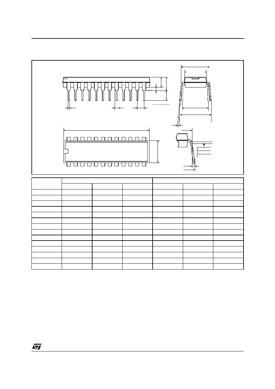
PACKAGE MECHANICAL DATA
24 PINS - PLASTIC DIP (SHRINK)
Dimensions
Millimeters
Inches
Min.
Typ.
Max.
Min.
Typ.
Max.
A
5.08
0.20
A1
0.51
0.020
3.05
3.30
4.57
0.120
0.130
0.180
B
0.36
0.46
0.56
0.0142
0.0181
0.0220
B1
0.76
1.02
1.14
0.030
0.040
0.045
C
0.23
0.25
0.38
0.0090
0.0098
0.0150
D
22.61
22.86
23.11
0.890
0.90
0.910
E
7.62
8.64
0.30
0.340
E1
6.10
6.40
6.86
0.240
0.252
0270
e
1.778
0.070
e1
7.62
0.30
e2
10.92
0.430
e3
1.52
0.060
L
2.54
3.30
3.81
0.10
0.130
0.150
S
D
I
P
24.
T
B
L
Information furnished is believed to be accurate and reliable. However, STMicroelectronics assumes no responsibility for the
consequences of use of such information nor for any infringement of patents or other rights of third parties which may result from
its use. No licence is granted by implication or otherwise under any patent or patent rights of STMicroelectronics. Specifications
mentioned in this publication are subject to change without notice. This publication supe rsedes and replaces all information
previously supplied. STMicroelectronics products are not authorized for use as critical comp onents in lifesupport devicesor systems
without express written approval of STMicroelectronics.
The ST logo is a trademark of STMicroelectronics
©
1998 STMicroelectronics - All Rights Reserved
Purchase of I
2
C Components of STMicroelectronics, conveys a license under the Philips I
2
C Patent.
Rights to use these components in a I
2
C system, is granted provided that the system conforms to
the I
2
C Standard Specifications as defined by Philips.
STMicroelectronics GROUP OF COMPANIES
Australia - Brazil - Canada - China - France - Germany - Italy - Japan - Korea - Malaysia - Malta - Mexico - Morocco - The Netherlands
Singapore - Spain - Sweden - Switzerland - Taiwan - Thailand - United Kingdom - U.S.A.
TDA9203A
13/13