TDA9203A
I
2
C BUS CONTROLLED 70MHz RGB PREAMPLIFIER
June 1998
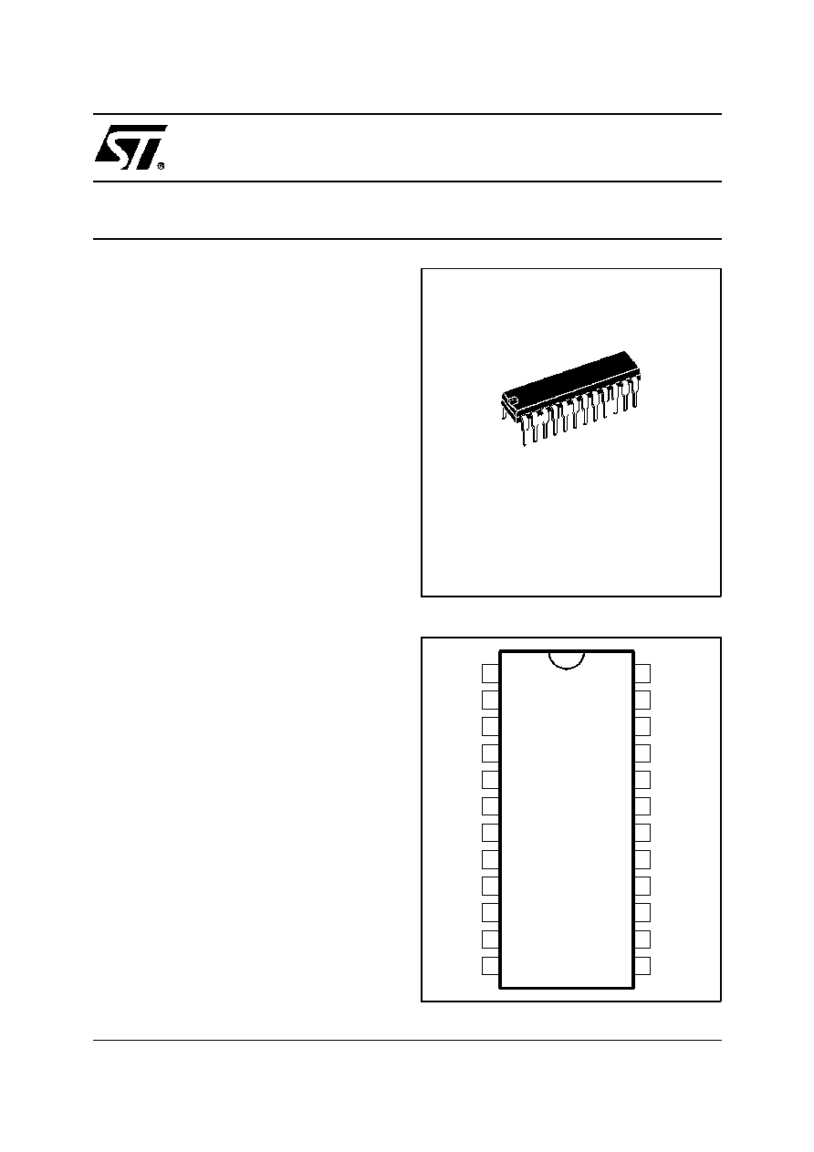
SHRINK 24
(Plastic Package)
ORDER CODE : TDA9203A
.
70MHz TYPICAL BANDWIDTH AT 4V
PP
OUT-
PUT WITH 12pF CAPACITIVE LOAD
.
5.5ns TYPICAL RISE/FALL TIME AT 4V
PP
OUTPUT WITH 12pF CAPACITIVE LOAD
.
POWERFULL OUTPUT DRIVE CAPABILITY
.
BRT, CONT, DRIVE, OUTPUT DC LEVEL,
OSD CONTRAST, BACK-PORCH CLAMPING
PULSE WIDTH ARE I
2
C BUS CONTROLLED
.
INTERNAL
BACK-PORCH
CLAMPING
PULSE GENERATOR
.
OSD WHITE BALANCE TRACKING
.
INTERNAL OSD SWITCHES
.
BLANKING AND FAST-BLANKING INPUTS
.
VERY LARGE DRIVE ADJUSTMENT RANGE
(48dB)
.
SEMI-TRANSPARENT BACKGROUND ON
OSD PICTURE
.
ABL CONTROL
DESCRIPTION
The TDA9203A is a digitaly controlled wideband
video preamplifier intended for use in mid range
color monitor. All controls and adjustments are
digitaly performed thanks to I
2
C serial bus. Con-
trast, brightness and DC output level of RGB sig-
nals are common to the 3 channels and drive
adjustment is separate for each channel. Three I
2
C
gain controlled OSD inputs can be switched with
RGB signals using fast blanking command. Clamp-
ing of RGB signals is performed thanks to a flexible
integrated system. The white balance adjustment
is effective on brightness, video and OSD signals.
The TDA9203A works for application using AC or
DC coupled CRT driver.
The ABL input provides a 12dB Max. attenuation
on the current contrast value according average
beam limitation voltage.
Because of its features and due to component
saving the TDA9203A leads to a very performant
and cost effective application.
1
2
3
4
5
6
7
8
9
10
20
19
18
17
16
15
14
13
24
23
22
21
11
12
HSYNC
PV
CC1
OUT1
PGND1
PV
CC2
OUT2
PGND2
PV
CC3
OUT3
PGND3
BLK
FBLK
IN1
OSD1
AV
DD
IN2
OSD2
AGND
IN3
OSD3
ABL
LGND
SDA
SCL
920
3A
-
01.
E
P
S
PIN CONNECTIONS
1/13

Name
Pin
Type
Fun ction
IN1
1
I
1
st
Channel Main Picture Input
OSD1
2
I
1
st
Channel OSD Input
AV
DD
3
I
12V Analog V
DD
IN2
4
I
2
nd
Channel Main Picture Input
OSD2
5
I
2
nd
Channel OSD Input
AGND
6
I/O
Analog Ground
IN3
7
I
3
rd
Channel Main Picture Input
OSD3
8
I
3
rd
Channel OSD Input
ABL
9
I
ABL Input
LGND
10
I/O
Logic Ground
SDA
11
I/O
Serial Data Line
SCL
12
I
Serial Clock Line
Name
Pin
Type
Function
FBLK
13
I
Fast Blanking Input
BLK
14
I
Blanking Input
PGND3
15
I/O
3
rd
Channel Power Ground
OUT3
16
O
3
rd
Channel Output
PV
CC3
17
I
3
rd
Channel Power V
CC
PGND2
18
I/O
2
nd
Channel Power Ground
OUT2
19
O
2
nd
Channel Output
PV
CC2
20
I
2
nd
Channel Power V
CC
PGND1
21
I/O
1
st
Channel Power Ground
OUT1
22
O
1
st
Channel Output
PV
CC1
23
I
1
st
Channel Power V
CC
HSYNC
24
I
Horizontal Synch Input
9203A
-
0
1
.
T
B
L
PIN DESCRIPTION
1
2
3
4
5
6
7
8
9
10
11
12
13
14
15
16
17
18
19
20
21
22
23
24
CLAMP
V
REF
AV
DD
IN1
AGND
IN2
BRIGHTNESS
IN3
OUTPUT
STAGE
DRIVE
8 bits
BPCP
PV
CC1
FBLK
BLK
OUT1
PGND1
PV
CC2
OUT2
PGND2
OUT3
PGND3
PV
CC3
ABL
LGND
I
2
C
BUS
DECODER
D/A
LATCHES
BPCP
SCL
SDA
HSYNC
OSD
OSD1
OSD2
OSD3
GREEN CHANNEL
BLUE CHANNEL
I
2
C
V
REF
OUTPUT
DC LEVEL
ADJUST
TDA9203A
CONTRAST
CONT
92
03A
-
0
2.
E
P
S
BLOCK DIAGRAM
TDA9203A
2/13

BLK
HSYNC
BPCP
Internal pulse width is controlled by I
2
C
92
03A
-
0
3.
E
P
S
Figure 1
FUNCTIONAL DESCRIPTION
Input Stage
The R, G and B signals must be fed to the three
inputs through coupling capacitors (100nF).
The maximum input peak-to-peak video amplitude
is 1V.
The input stage includes a clamping function. This
clamp is using the input serial capacitor as "mem-
ory capacitor" and is gated by an internally gener-
ated "Back-Porch-Clamping-Pulse (BPCP)".
The synchronization edge of the BPCP is selected
according bit 0 of register R8.
When B0R8 is set to 1, the BPCP is synchronized
on the leading edge of the blankingpulse BLKinputs
on Pin14 (seeFigure1). B7R8 allows to use positive
or negative blanking signal on Pin 14. At power on
reset TDA9203A use only positive blanking.
When B0R8 is clear to 0, the BPCP is synchronized
on the second edge of the horizontal pulse HSYNC
inputs on Pin 24. An automatic function allows to
use positive or negative horizontal pulse on Pin 24
(see Figure 2).
In both case BPCP width is adjustable by I
2
C, B1
and B2 of register R8 (see R8 Table P8).
Contrast Adjustment (8 bits)
The contrast adjustment is made by controlling
simultaneously the gain of three internal variable
gain amplifiers through the I
2
C bus interface.
The contrast adjustment allows to cover a typical
range of 48dB.
ABL Control
The TDA9203A I
2
C preamplifier provides an ABL
input (automatic beam limitation) to attenuat e
R,G,B video signals according to beam intensity.
The operating range is 2.5V typicaly, from 5.3V to
2.8V. A typical 12dB Max. attenuation is applied to
the signal whatever the current gain is. Refer to
Figure 3 for ABL input attenuation range.
In case of software control, the ABL input must be
pulled to AV
DD
through a resistor to limit power
consumption (see Figure 11).
ABL input voltage must not exceeed AV
DD
. Input
resistor is 10k
and equivalent schematic given in
Figure 11.
HSYNC
BPCP
Internal pulse width is controlled by I
2
C
920
3A
-
04.
E
P
S
Figure 2
Brightness Adjustment (8 bits)
As for the contrast adjustment, the brightness is
controlled by I
2
C.
The brightness function consists to add the same
DC offset to the three R, G, B signals after contrast
amplification. This DC-Offset is present only out-
side the blanking pulse (see Figure 4).
The DC output level during the blanking pulse, is
forced to "INFRA-BLACK" level (V
DC
).
Drive Adjustment (3 x 8 bits)
In order to adjust the white balance , the TDA9203A
offers the possibility to adjust separately the overall
gain of each complete video channel. The gain of
each channel is controlled by I
2
C (8bits each).
The very large drive adjustment range (48dB) allows
different standard or custom color temperature.
It can also be used to adjust the output voltages at
the optimum amplitude to drive the C.R.T drivers,
keepingthe whole contrast control for end-useronly.
The drive adjustment is located after the CON-
TRAST, BRIGHTNESS and OSD switch blocks, so
that the white balance will remains correct when
BRT is adjusted, and will also be correct on OSD
portion of the signal.
2
0
-2
-4
-6
-8
-10
-12
-14
1
2
3
4
5
6
7
8
9
Attenuation (dB)
V
IN
(V)
9203
A
-
0
X
.
E
P
S
Figure 3
TDA9203A
3/13

FUNCTIONAL DESCRIPTION (continued)
OSD Inputs
The TDA9203A includes all the circuitry necessary
to mix OSDsignals into the RGB main-picture. Four
pins are dedicated to this function as follow.
Three TTL RGB On Screen Display inputs (Pin 2,
5 and 8). These three inputs are connected to the
three outputs of the corresponding ON-SCREEN-
DISPLAY processor (ex : STV942x).
One Fast Blanking Input (FBLK, Pin 13) which is
also connected to the FBLK output of the same
ON-SCREEN-DISPLAY processor.
When a high level is present on FBLK, the IC will
acts as follow :
- The three main picture RGB input signals are
internally switched to the internal input clamp
reference voltage.
- The three output signals are set to voltages cor-
respondingto the state (0 or 1) on the three OSD
inputs (see Figure 4).
Example :
If FBLK = 1 and OSD1, OSD2, OSD3) = 1, 0, 1
respectively.
Then OUT1, OUT2, OUT3 will be equal to V
OSD
,
V
BRT
, V
OSD
,
where : V
BRT
= V
BLACK
+ BRT, V
OSD
= V
BRT
+ OSD
BRT is the brightness DC level I
2
C adjustable.
OSD is the On-Screen Display signal value I
2
C
adjustable from 0V to 5.5V
PP
by step of 0.36V.
Semi-transparent function is controlled thanks to
Bit 6 of R8 register (see Table 1).
When semi-transparent mode is activated, video
signal is divided by 2 (CONT).
Table 1
FBLK OSD1 OSD2 OSD3 B6R8
Output
Signal (OUTn)
0
x
x
x
0
Video
1
x
x
x
0
OSD (1)
0
x
x
x
1
Video
1
0
x
x
1
OSD
1
x
1
x
1
OSD
1
x
x
0
1
OSD
1
1
0
1
1
Semi-trans-
parent (2)
Notes : 1. All OSD colors are displayed.
2. One OSD color is displayed as semi-transparent video
without effect on brightness and DC level adjustment.
Output Stage
The three output stagesincorporate threefunctions
which are :
- The blanking stage : When high level is applied
to the BLK input (Pin 14), the three outputs are
switched to a voltage which is 400mV lower than
the BLACK level. The black level is the output
voltage with minimum brightness when input sig-
nal video amplitude is equal to "0".
- The output stage itself : It is a large bandwidth
output amplifier which allow to deliver up to 5V
PP
on the three outputs (for 0.7V video signal on the
inputs).
- The output CLAMP : The IC also incorporates
three internal output clamp (sample and hold
system) which allow to DC shift the three output
signals. The DC output voltage is adjustable
through I
2
C with 4 bits. Practicaly, the DC output
level allow to adjust the BLK level (V
DC
= 400mV
under V
BLACK
) from 0.9V to 2.9V with 12 x 165mV.
The overall waveforms of the output signal accord-
ing to the different adjustment are shown in Fig-
ures 4 and 5.
Serial Interface
The 2-wires serial interface is an I
2
C interface.
The slave address of the TDA9203A is DC (in
hexadecimal).
A6
A5
A4
A3
A2
A1
A0
W
1
1
0
1
1
1
0
0
Data Transfer
The host MCU can write data into the TDA9203A
registers. Read mode is not available.
To write data into the TDA9203A, after a start, the
MCU must send (see Figure 6) :
- The I
2
C addressslave byte with a low level for the
R/W bit.
- The byte of the internal register address where
the MCU wants to write data(s).
- The data.
All bytes are sent MSB bit first and the write data
transter is closed by a stop.
TDA9203A
4/13

HSYNC
V
CONT
(4)
BPCP
BLK
Video IN
FBLK
OSD IN
V
OSD
(5)
V
BRT
(3)
V
BLACK
(2)
V
DC
(1)
CONT
OSD
BRT
0.4V fixed
V
OUT1
, V
OUT2
, V
OUT3
Notes : 1.
V
DC
= 0.5 to 2.5V
2.
V
BLACK
= V
DC
+ 0.4V
3.
V
BRT
= V
BLACK
+ BRT (with BRT = 0 to 2.5V)
4.
V
CONT
= V
BRT
+ CONT with CONT = k x Video IN (CONT = 5V
P P
max. for V
IN
= 0.7V
PP
)
5.
V
OSD
= V
BRT
+ OSD with OSD = k1 x OSDIN (OSD max. = 5.5V
PP
, OSD min. = 360mV
PP
)
9203
A
-
0
6
.
E
P
S
Figure 4 : Waveforms VOUT, BRT, CONT, OSD
HSYNC
V
CONT
BPCP
BLK
Video IN
FBLK
OSD IN
V
OSD
V
BRT
V
BLACK
V
DC
V
OUT1
, V
OUT2
, V
OUT3
Note : 1. Drive adjustment modifies the following voltages : V
CONT
, V
BRT
and V
OSD
.
Drive adjustment do not modify the following voltages : V
DC
and V
BLACK
.
Two exemples
of drive adjustment
(1)
9203
A
-
0
7
.
E
P
S
Figure 5 : Waveforms (DRIVE adjustment)
FUNCTIONAL DESCRIPTION (continued)
SCL
W
A7
A6
A5
A4
A3
A2
A1
A0
SDA
Register Address
ACK
ACK
I
2
C Slave Address
Start
D7
D6
D5
D4
D3
D2
D1
D0
Data Byte
ACK
Stop
9203A
-
0
8
.
E
P
S
Figure 6 : I
2
C Write Operation
TDA9203A
5/13