
Version 4.2
March 2000
1/22
TDA9207
150 MHz PIXEL VIDEO CONTROLLER FOR MONITORS
INCLUDING CUT-OFF INPUTS
FEATURE
s
150 MHZ PIXEL RATE
s
2.7 ns RISE AND FALL TIME
s
I
2
C BUS CONTROLLED
s
GREY SCALE TRACKING VERSUS BRIGHT-
NESS
s
OSD MIXING
s
NEGATIVE FEED-BACK FOR DC COUPLING
APPLICATION
s
INTERNAL POSITIVE FEED-BACK FOR LCD
APPLICATION
s
0.5~4.5 V DACs FOR BLACK LEVEL RESTO-
RATION (AC-COUPLING APPLICATION) OR
CUT-OFF CONTROLS (FOR DC-COUPLING
APPLICATION USING THE ST AMPLIFIERS
TDA9533/9530)
s
BEAM CURRENT ATTENUATION (ABL)
s
PEDESTRAL
CLAMPING
ON
OUTPUT
STAGE
s
POSSIBILITY OF LIGHT OR DARK GREY
OSD BACKGROUND
s
OSD INDEPENDENT CONTRAST CONTROL
s
ADJUSTABLE BANDWIDTH
s
INPUT BLACK
LEVEL
CLAMPING WITH
BUILT-IN CLAMPING PULSE
s
STAND-BY MODE
s
5 V TO 8 V POWER SUPPLY
s
SYNC CLIPPING FUNCTION (SOG)
DESCRIPTION
The TDA9207 is an I
2
C Bus controlled RGB pre-
amplifier designed for Monitor application, able to
mix the RGB signals coming from any OSD de-
vice. The usual Contrast, Brightness, Drive and
Cut-Off Controls are provided.
In addition, it includes the following features:
� OSD contrast,
� Bandwidth adjustment,
� Grey background,
� Internal back porch clamping pulse generator.
The RGB incoming signals are amplified and
shaped to drive any commonly used video amplifi-
ers without intermediate follower stages. Even
though encapsulated in a 24-pin package only,
this IC allows any kind of CRT Cathode coupling :
� AC coupling with DC restore,
� DC coupling with Feed-back from Cathodes,
� DC coupling with Cut-Off controls of the Video
amplifier (ST Amplifiers TDA9533/9530).
As for any ST Video pre-amplifier, the TDA9207 is
able to drive a real load without any external inter-
face.
One of the main advantages of ST devices is their
ability to sink and source currents while most of
the devices from our competitors have problems
to sink large currents.
These driving capabilities combined with an origi-
nal output stage structure suppress any static cur-
rent on the output pins and therefore reduce dra-
matically the power dissipation of the device.
Extensive integration combined with high perform-
ance and advanced features make the TDA9207
one of the best choice for any CRT Monitor in the
14" to 17" range.
Perfectly matched with the ST Video Amplifiers
TDA9530/33, these 2 products offer a complete
solution for high performance and cost-optimized
Video Board Application.
SHRINK DIP24
(Shrink Plastic Package)
ORDER CODE: TDA9207
1

TDA9207
2/22
1 - PIN CONNECTIONS
2 - PIN DESCRIPTION
Pin Number
Symbol
Description
1
IN1
Red Video Input
2
ABL
ABL Input
3
IN2
Green Video Input
4
GNDL
Logic Ground
5
IN3
Blue Video Input
6
GNDA
Analog Ground
7
V
CCA
Analog V
CC
(5V)
8
NC
Not Connected
9
OSD1
Red OSD Input
10
OSD2
Green OSD Input
11
OSD3
Blue OSD Input
12
FBLK
Fast Blanking
13
SCL
SCL
14
SDA
SDA
15
CO2/FB2
Green Cut-off Output/Feedback Input
16
CO3/FB3
Blue Cut-off Output/Feedback Input
17
OUT3
Blue Video Output
18
GNDP
Power Ground
19
OUT2
Green Video Output
20
V
CCP
Power V
CC
(5 V to 8 V)
21
OUT1
Red Video Output
22
CO1/FB1
Red Cut-off Output/Feedback Input
23
HSYNC
BPCP
HSYNC
BPCP
24
BLK
Blanking Input
BLK
IN1
ABL
IN2
GNDL
IN3
GNDA
V
CCA
NC
OSD1
OSD2
OSD3
FBLK
HSYNC or BPCP
CO1/FB1
OUT1
V
CCP
OUT2
GNDP
OUT3
CO3/FB3
CO2/FB2
SDA
SCL
1
2
3
4
5
6
7
8
9
10
11
12
24
23
22
21
20
19
18
17
16
15
14
13

TDA9207
3/22
3 - BLOCK DIAGRAM
4 - FUNCTIONAL DESCRIPTION
4.1 RGB Input
The three RGB inputs have to be supplied through
coupling capacitors (100 nF).
The maximum input peak-to-peak video amplitude
is 1 V.
The input stage includes a clamping function. The
clamp uses the input serial capacitor as a "memo-
ry capacitor".
To avoid a discharge of the serial capacitor during
the line (due to leakage current), the input voltage
is referenced to the ground.
The clamp is gated by an internally generated
"Back Porch Clamping Pulse" (BPCP). Register 8
allows to choose the way to generate this BPCP
(see Figure 1).
When bit 0 is set to 0, the BPCP is synchronized
on the trailing or leading edge of HSYNC (Pin 23)
(bit 1 = 0: trailing edge, bit 1 = 1: leading edge).
BLK
FBLK
VCCP
OUT1
CO1/FB1
GNDP
OUT2
CO2/FB2
OUT3
CO3/FB3
IN1
IN2
IN3
ABL
GNDL
GNDA
VCCA
NC
HSYNC
SDA SCL
OSD1
OSD2
OSD3
or BPCP
TDA9207
20
12
24
1
3
5
2
4
6
7
8
23
14
13
9
10
11
16
17
15
19
18
22
21
Output Clamp Pulse
(OCL)
Output
Stage
Drive
Contrast
V
REF
Clamp
Green Channel
Blue Channel
Contrast/8bit
Latches
I
2
C
Bus
Decoder
D/A
BPCP
OSD
Cont.
4bits
Drive
3x8bits
Brightness
8bits
V
REF
Output
DC Level
4bits
I C
Cut-off
8bits
See Figure 12 for complete BPCP and OCL generation diagram

TDA9207
4/22
Additionally, the IC automatically works with either
positive or negative HSYNC pulses.
� When bit 0 is set to 1, BPCP is synchronized on
the leading edge of the blanking pulse BLK
(Pin 24). One can use a positive or negative
blanking pulse by programming bit 0 in
Register 9 (See I
2
C Table 3).
� BPCP width can be adjusted with bit 2 and 3 (see
Register 8, I
2
C table 2).
� If the application already provides the Back
Porch Clamping Pulse, bit 4 must be set to 1
(providing a direct connection between Pin 23
and internal BPCP).
4.2 Synchro Clipping Function
This function is available on channel 2 (Green
Channel). When using the Sync On Green (SOG)
(Synchro pulse included in the green channel in-
put) the synchro clipping function must be activat-
ed (bit 7 set to 1 in register 9) in order to keep the
right green output levels and avoid unbalanced
colours.
4.3 Blanking Input
The Blanking pin (FBLK) is TTL compatible.
The Blanking pulse can be:
� positive or negative
� line or Composite-type (but not Frame-type).
4.4 Contrast Adjustment (8 bits)
The contrast adjustment is made by controlling si-
multaneously the gain of the three internal amplifi-
ers through the I
2
C bus interface. Register 1 al-
lows the adjustment in a range of 48 dB.
Figure 1.
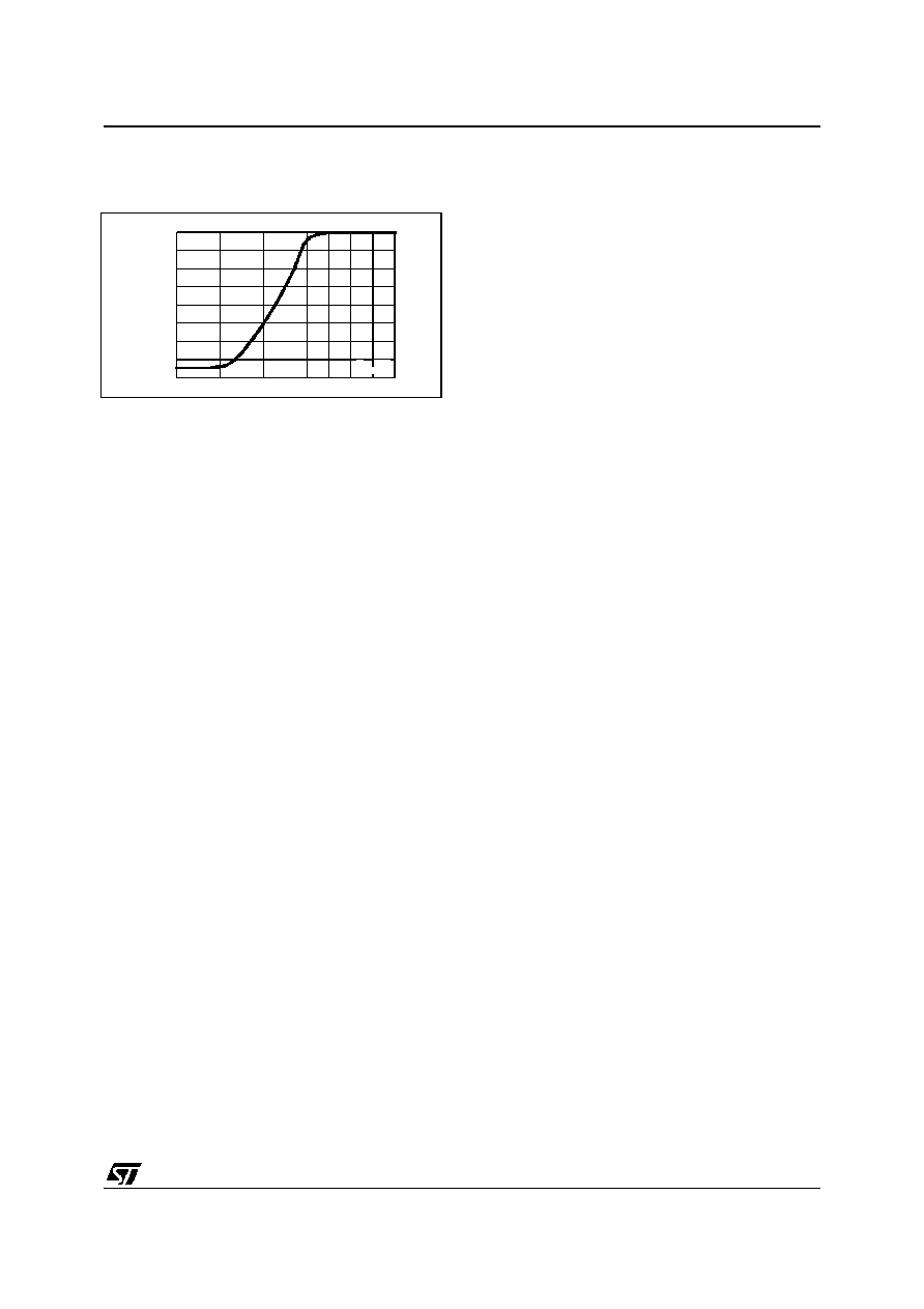
4.5 ABL Control
The TDA9207 includes an ABL (automatic beam
limitation) input to attenuate the RGB Video sig-
nals depending on the beam intensity.
The operating range is 2 V (from 3 V to 1 V). A typ-
ical 15 dB maximum attenuation is applied to the
output signal whatever the contrast adjustment is.
(See Figure 2 ).
When the ABL feature is not used, the ABL input
(Pin 2) must be connected to a 5 V supply voltage.
R8b0=0 and R8b1=0
HSYNC/BPCP (Pin23)
Internal BPCP
R8b0=0 and R8b1=1
HSYNC/BPCP (Pin23)
Internal BPCP
R8b0=1
BLK (Pin24)
Internal BPCP
R8b4 =1
HSYNC/BPCP (Pin23)
Internal BPCP
TDA9207
5/22
Figure 2.
4.6 Brightness Adjustment (8 bits)
Brightness adjustment is controlled by the I
2
C Bus
via Register 2. It consists of adding the same DC
voltage to the three RGB signals, after contrast ad-
justment. When the blanking pulse equals 0, the
DC voltage is set to a value which can be adjusted
between 0 and 2V with 8mV steps (see Figure 3).
The DC output level is forced to the "Infra Black"
level (V
DC
) when the blanking pulse is equal to 1.
4.7 Drive Adjustment (3 x 8 bits)
In order to adjust the white balance, the TDA9207
offers the possibility of adjusting separately the
overall gain of each channel thanks to the I
2
C bus
(Registers 3, 4 and 5).
The very large drive adjustment range (48 dB) al-
lows different standards or custom color tempera-
tures.
It can also be used to adjust the output voltages at
the optimum amplitude to drive the CRT drivers,
keeping the whole contrast control for the end-
user only.
The drive adjustment is located after the Contrast,
Brightness and OSD switch blocks, so it does not
affect the white balance setting when the BRT is
adjusted. It also operates on the OSD portion of
the signal.
4.8 OSD Inputs
The TDA9207 allows to mix the OSD signals into
the RGB main picture. The four pins dedicated to
this function are the following:
� Three TTL RGB inputs (Pins 9, 10, 11) connect-
ed to the three outputs of the corresponding OSD
processor.
� One TTL fast blanking input (Pin 12) also con-
nected to the FBLK output of the OSD processor.
When a high level is present on the FBLK, the IC
acts as follows:
� The three main picture RGB input signals (IN1,
IN2, IN3) are internally switched to the internal
input clamp reference voltage.
� The three output signals are set to the voltage
corresponding to the three OSD input logic
states (0 or 1). (See Figure 3).
If the OSD input is at low level, the output and
brightness voltages (V
BRT
) are equal.
If the OSD input is at high level, the output voltage
is V
OSD
, where V
OSD
= V
BRT
+ OSD and OSD is
an I
2
C bus-controlled voltage.
OSD varies between 0 V to 4.9 V by 320 mV steps
via Register 7 (4 bits). The same variation is ap-
plied simultaneously to the three channels provid-
ing the OSD contrast.
The grey color can be obtained on output signals
when:
� OSD1 = 1, OSD2 = 0 and OSD3 = 1,
� A special bit (bit 5 or 6) in Register 9 is set to 1.
If R9b5 is set to 1, light grey is obtained on output.
If R9b6 is set to 1, dark grey is obtained on output.
In the case where R9b5 and R9b6 are set to 0, the
normal operation is provided on output signals.
4.9 Output Stage
The overall waveforms of the output signal are
shown in Figure 3 and Figure 4. The three output
stages, which are large bandwidth output amplifi-
ers, are able to deliver up to 4.4 V
PP
for 0.7 V
PP
on
input.
When a high level is applied on the BLK input
(Pin 24), the three outputs are forced to "Infra
Black" level (V
DC
) thanks to a sample and hold cir-
cuit (described below).
The black level (which is the output voltage out-
side the blanking pulse with minimum brightness
and no Video input signals) is 400 mV higher than
V
DC
.
The brightness level (V
BRT
) is then obtained by
programming register 2 (see I
2
C table 1).
The sample and hold circuit is used to control the
"Infra Black" level in the range of 0.5 V to 2.5 V via
Register 6 (in case of AC coupling) or Registers
10, 11, 12 (in case of DC coupling) .
This sampling occurs during an internal pulse
(OCL) generated inside the blanking pulse win-
dow.
Refer to "CRT cathode coupling" part for further
details.
5
0
-2
-4
-6
-8
-10
-12
-14
-16
Attenuation (dB)
0
V
ABL
(V)
4
3
2
1