TDE1737
TDF1737
October 1991
INTERFACE CIRCUIT - RELAY AND LAMP-DRIVER
.
HIGH OUTPUT CURRENT
.
ADJUSTABLE SHORT-CIRCUIT PROTEC-
TION
.
THERMAL PROTECTION WITH HYSTERESIS
TO AVOID THE INTERMEDIATE OUTPUT LEV-
ELS
.
LARGE SUPPLY VOLTAGE RANGE : + 8 V to
+ 45 V
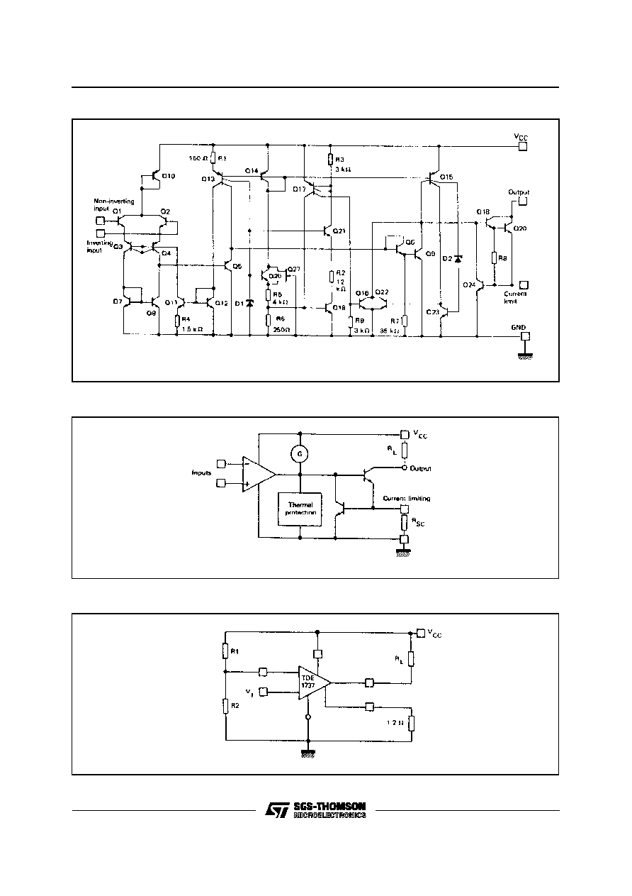
DESCRIPTION
The TDE1737-TDF1737 is a monolithic amplifier
designed for high current and high voltage applica-
tions, specifically to drive lamps, relays and control
of stepper motors.
This device is essentially blow-out proof. Current
limiting is available to limit the peak output current
to a safe value, the adjustment only requires one ex-
ternal resistor. In addition, thermal shut down is pro-
vided to keep the I.C. from overheating. If internal
dissipation becomes too great, the driver will shut
down to prevent excessive heating.
The output is also protected against short-circuits
with the positive power supply.
The device operates over a wide range of supply
voltages from standard
±
15 V operational amplifier
supplies down to the single + 12 V or + 24 used for
industrial electronic systems.
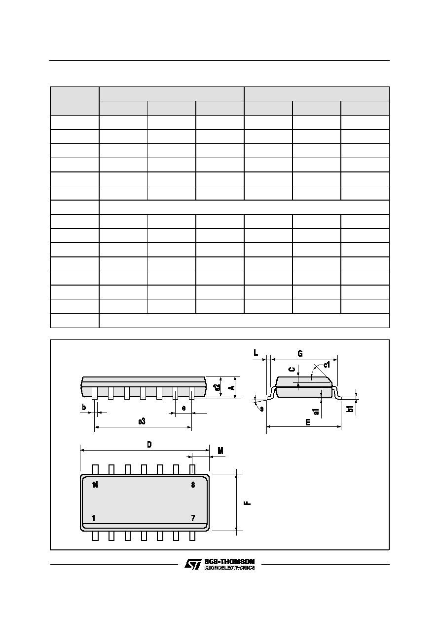
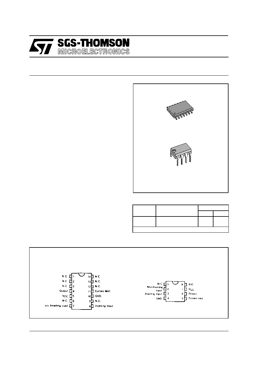
MINIDIP
DP SUFFIX
SO14
FP SUFFIX
ORDER CODES
Part
Number
Temperature
Range
Package
DP
FP
TDE1737
TDF1737
≠ 25
∞
C to + 85
∞
C
≠ 40
∞
C to + 85
∞
C
∑
∑
∑
∑
Example : TDE1737DP
PIN CONNECTIONS (top views)
SO-14
MINIDIP
1/7
ABSOLUTE MAXIMUM RATINGS
Symbol
Parameter
Value
Unit
V
s
Supply Voltage
50
V
V
I
Input Voltage
50
V
V
ID
Differential Input Voltage
50
V
I
O
Output Current
1000
mA
P
tot
Power Dissipation
Internally Limited
W
T
oper
Operating Free≠air Temperature Range for TDE1737
≠ 25 to + 85
∞
C
T
oper
Operating Free≠air Temperature Range for TDF1737
≠ 40 to + 85
∞
C
T
stg
Storage Temperature Range
≠ 65 to + 150
∞
C
THERMAL CHARACTERISTICS
Symbol
Parameter
Value
Unit
R
th(j-c)
Maximum Junction-case Thermal Resistance MINIDIP
50
∞
C/W
R
th(j-a)
Maximum Junction-ambient Thermal Resistance
MINIDIP
120
∞
C/W
Junction-ceramic Substrate (case glued to substrate) SO14
90
∞
C/W
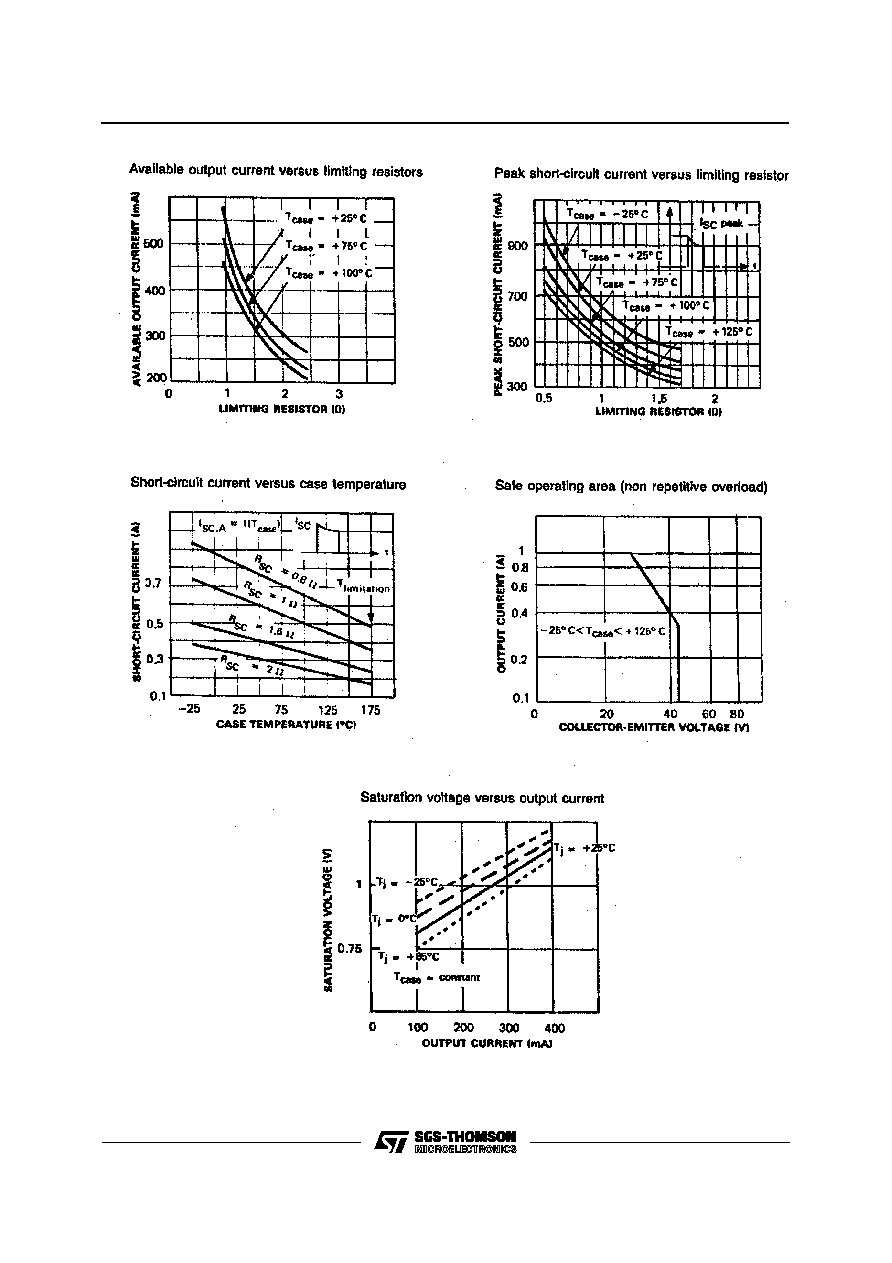
ELECTRICAL CHARACTERISTICS
TDE1737 ≠ 25
∞
C
T
amb
+ 85
∞
C, + 8 V
V
CC
+ 45 V, I
O
300 mA, T
j
+ 150
∞
C
(unless otherwise specified)
TDF1737 ≠ 40
∞
C
T
amb
+ 85
∞
C, + 8 V
V
CC
+ 45 V, I
O
300 mA, T
j
150
∞
C
Symbol
Parameter
Min.
Typ.
Max.
Unit
V
IO
Input Offset Voltage ≠ (note 1)
≠
2
50
mV
I
IB
Input Bias Current
≠
0.1
1.5
µ
A
I
CC
Supply Current (V
CC
= + 24 V, I
O
= 0)
≠
3
5
mA
V
CM
Common≠mode Input Voltage Range
2
≠
V
CC
≠2
V
I
SC
Short≠circuit Current Limit (R
SC
= 1.5
, T
case
= + 25
∞
C)
≠
500
≠
mA
V
CC
≠V
O
Output Saturation Voltage (output low)
(V
I
+
≠ V
I
≠
50 mV I
O
= 300 mA, R
SC
= 0)
≠
1
1.5
V
I
OL
Output Leakage Current
(output high) (V
O
= V
CC
= + 24 V, T
amb
= + 25
∞
C)
≠
≠
10
µ
A
Notes : 1. The offset voltage given is the maximum value of input voltage required to drive the output voltage within 2 V of
the ground or the supply voltage.
2. Devices bonded on a 40 cm
2
glass-epoxy printed circuit 0.15 cm thick with 4 cm
2
of cooper.
TDE1737 - TDF1737
2/7