 | –≠–ª–µ–∫—Ç—Ä–æ–Ω–Ω—ã–π –∫–æ–º–ø–æ–Ω–µ–Ω—Ç: TDE3237DP | –°–∫–∞—á–∞—Ç—å:  PDF PDF  ZIP ZIP |
TDE3237
INTELLIGENT POWER SWITCH
ADVANCE DATA
HIGH OUTPUT CURRENT
ADJUSTABLE SHORT-CIRCUIT PROTECTION
INTERNAL THERMAL PROTECTION WITH
HYSTERESIS TO AVOID THE INTERMEDI-
ATE OUTPUT LEVELS
LARGE SUPPLY VOLTAGE RANGE: 8 TO 30V
DESCRIPTION
The TDE3237 is a monolithic amplifier designed
for high-current and high-voltage applications,
specIally to drive lamps, relays and stepping mo-
tors.
The device is essentially blow-out proof. Current
limiting is available to limit the peak output current
to a safe value, the adjustment only requires one
external resistor. In addition, thermal shut down is
provided to keep the IC from overheating. If exter-
nal dissipation becomes too great, the driver will
shut down to prevent excessive heating.
The output is also protected from short-circuits
with the positive power supply.
The device operates over a wide range of supply
voltages from standard
±
15V operational amplifier
supplies down to the single 12V or 24V used for
industrial electronic systems.
November 1991
T
is advanced information on a new product now in development or undergoing evaluation. Details are subject to change without
This is advanced information on a new product now in development or undergoing evaluation. Details are subject to change without notice.
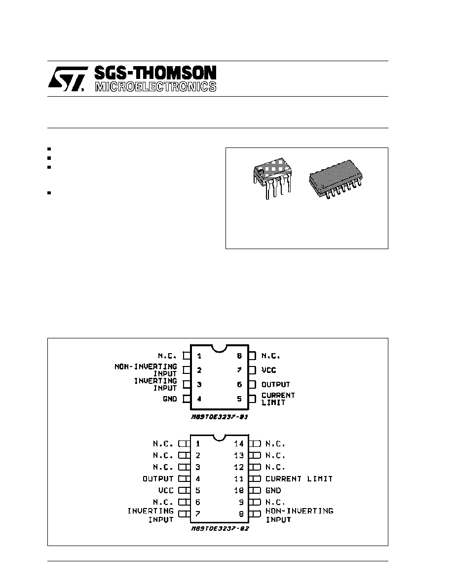
PIN CONNECTIONS
Minidip
SO14
ORDERING NUMBERS:
TDE3237DP
TDE3237FP
Minidip
SO14
1/7

ABSOLUTE MAXIMUM RATINGS
Symbol
Parameter
Value
Unit
V
CC
Supply Voltage
36
V
V
ID
Differantial Input Voltage
36
V
V
I
Input Voltage
36
V
I
O
Output Current
500
mA
P
tot
Power Dissipation
Internally Limited
W
T
stg
Storage Temperature Range
≠ 65 to + 150
∞
C
T
oper
Operating Free-air Temperature Range
≠ 25 to + 85
∞
C
THERMAL CHARACTERISTICS
Symbol
Parameter
Value
Unit
R
th(j-c)
Maximum Junction-case Thermal Resistance (note 1)
Minidip
50
∞
C/W
R
th(j-a)
Maximum Junction-ambient Thermal Resistance (note 1)
Minidip
120
∞
C/W
Junction-ceramic Substrate (case glued to substrate)
SO14
90
∞
C/W
Junction-ceramic Substrate (case glued to substrate, substrate temperature
maintened constant)
SO14
65
∞
C/W
Note :
1. Devices bonded on 40 cm glass-epoxy printed circuit 0.15cm thick with 4cm
2
of copper
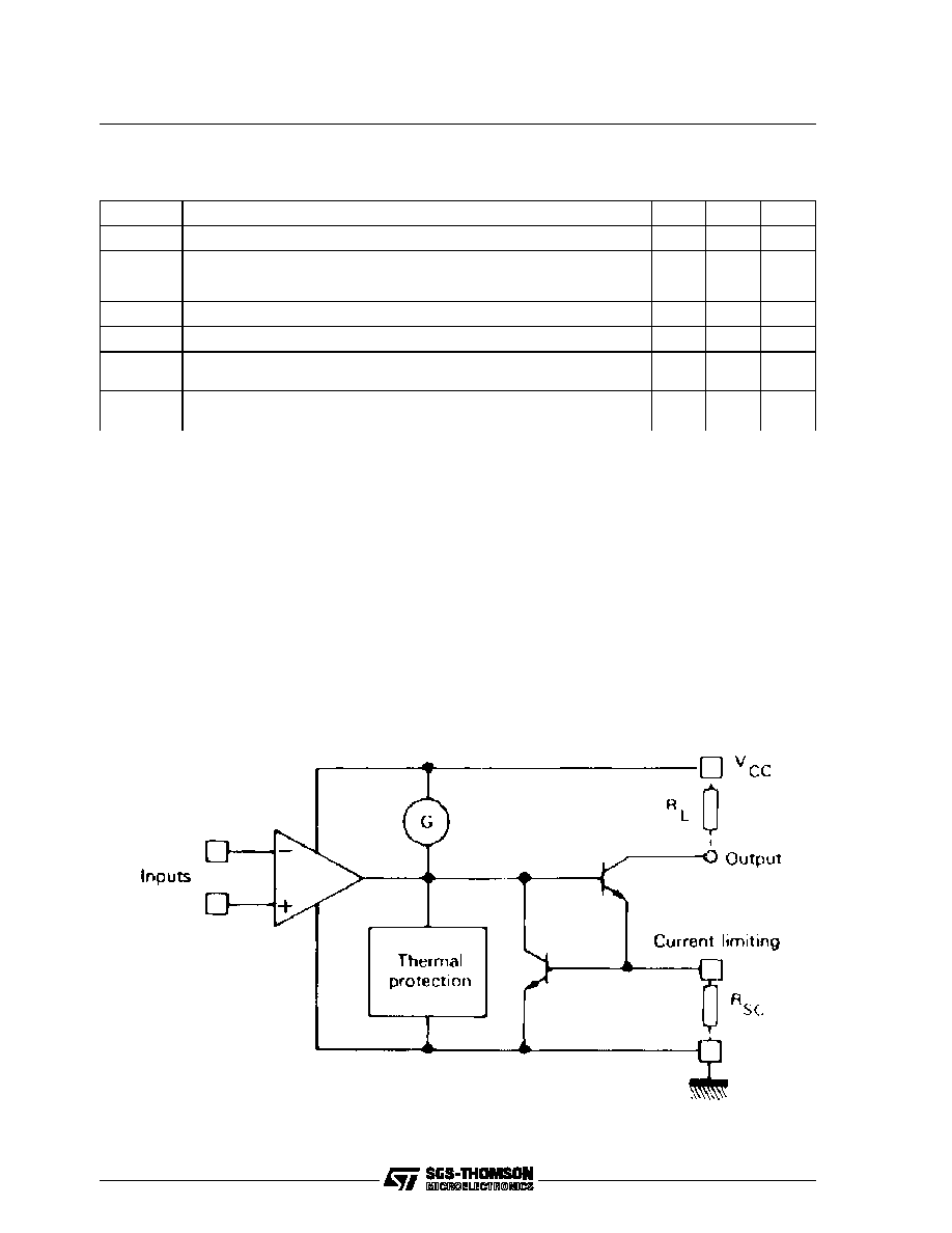
SCHEMATIC DIAGRAM
TDE3237
2/7
ELECTRICAL CHARACTERISTICS T
amb
= ≠ 25 to +85
∞
C, V
CC
= 8 to
30 V, unless otherwise speci-
fied (note 1).
Symbol
Parameter
Min.
Typ.
Max.
Unit
V
IO
Input Offset Voltage - (note 3)
≠
2
50
mV
I
IB
Input Bias Current
≠
0.1
1.5
µ
A
I
CC
Supply Current (V
CC
= + 24 V, I
O
= 0)
≠
3
5
mA
V
CM
Common-mode Input Voltage Range
2
≠
V
CC
≠2
V
I
SC
Short-circuit Current Limit (T
case
= + 25
∞
C, R
SC
= 3.3
)
≠
230
≠
-mA
V
CC
≠V
O
Output Saturation Voltage (output high)
(R
SC
= 0, V
I
+≠V
I
≠
50 mV, I
O
= 150 mA
≠
1
1.5
V
I
OL
Low Level Output Current
(V
O
= V
CC
= + 24 V T
amb
= + 25
∞
C)
≠
≠
100
µ
A
Notes :
2) For operating at high temperature, the TDE3237, must be derated based on a + 150 C maximum junction temperature and a junction-ambient
thermal as showed in the thermal characteristics data base.
3) The offset voltage given is the maximum value of input voltage required to drive the output voltage within 2 V of the ground or the supply
voltage.
SIMPLIFIED SCHEMATIC
TDE3237
3/7

TDE3237
4/7
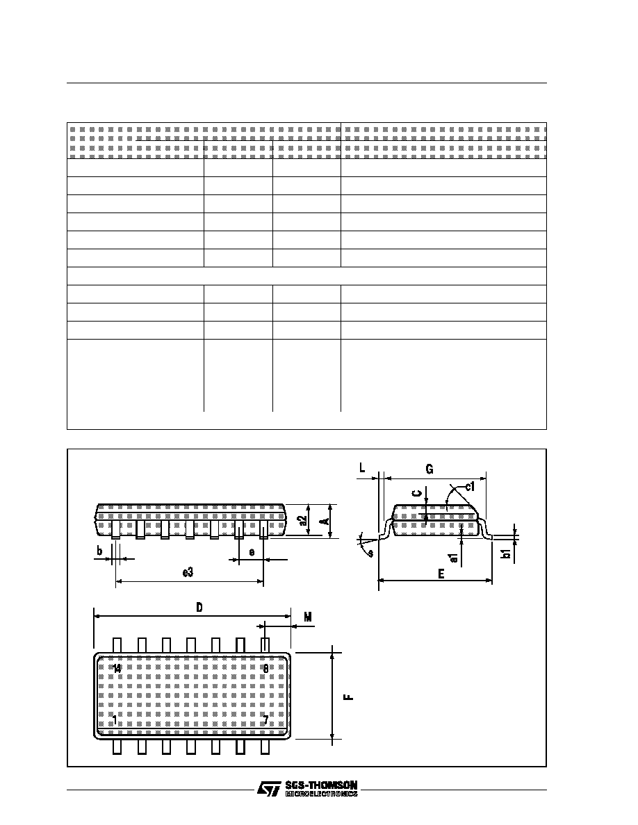
SO14 PACKAGE MECHANICAL DATA
DIM.
mm
inch
MIN.
TYP.
MAX.
MIN.
TYP.
MAX.
A
1.75
0.069
a1
0.1
0.25
0.004
0.009
a2
1.6
0.063
b
0.35
0.46
0.014
0.018
b1
0.19
0.25
0.007
0.010
C
0.5
0.020
c1
45 (typ.)
D
8.55
8.75
0.336
0.344
E
5.8
6.2
0.228
0.244
e
1.27
0.050
e3
7.62
0.300
F
3.8
4.0
0.15
0.157
L
0.4
1.27
0.016
0.050
M
0.68
0.027
S
8 (max.)
TDE3237
5/7