 | –≠–ª–µ–∫—Ç—Ä–æ–Ω–Ω—ã–π –∫–æ–º–ø–æ–Ω–µ–Ω—Ç: TDF1747DP | –°–∫–∞—á–∞—Ç—å:  PDF PDF  ZIP ZIP |
TDE1747
TDF1747
INTERFACE CIRCUIT ≠ RELAY AND LAMP ≠ DRIVER
OPEN GROUND PROTECTION
HIGH OUTPUT CURRENT
ADJUSTABLE
SHORT-CIRCUIT
PROTEC-
TION TO GROUND
THERMAL PROTECTION WITH HYSTERE-
SIS TO AVOID THE INTERMEDIATE OUT-
PUT LEVELS
LARGE SUPPLY VOLTAGE RANGE : + 10 V
TO + 45 V
SHORT-CIRCUIT PROTECTION TO V
CC
DESCRIPTION
The TDE/TDF1747 is a monolithic comparator de-
signed for high current and high voltage applica-
tions, specifically to drive lamps, relays, stepping
motors.
These device is essentially blow-out proof. Cur-
rent limiting is available to limit the peak output
current to safe values, the adjustment only re-
quires one external resistor. In addition, thermal
shut down is provided to keep the I.C. from over-
heating. If internals dissipation becomes too
great, the driver will shut down to prevent exces-
sive heating. TDE1747 has an open ground pro-
tection. The output is also protected from short-
circuits with the positive power supply.
The device operates over a wide range of supply
voltages from standard
±
15 V operational ampli-
fier supplies down to the single + 12 V or + 24
used for industrial electronic systems.
This is advanced information on a new product now in development or undergoing evaluation. Details are subject to change without notice.
November 1991
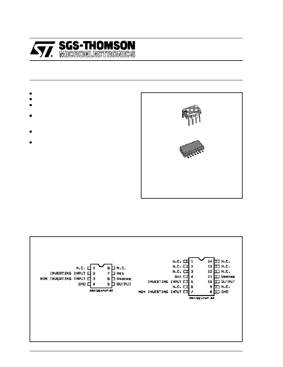
PIN CONNECTIONS (Top view)
Minidip (DP)
SO14 (FP)
ORDERING NUMBERS:
TDE1747DP
TDE1747FP
TDF1747DP
Minidip
SO14
1/11
ABSOLUTE MAXIMUM RATINGS
Symbol
Parameter
Value
Unit
V
CC
Supply Voltage
50 *
V
V
ID
Differantial Input Voltage
50
V
V
I
Input Voltage
50
V
I
O
Output Current
1
A
P
tot
Power Dissipation (T
amb
= + 25
∞
C)
Internally Limited
W
T
stg
Storage Temperature Range
≠ 65 to + 150
∞
C
T
oper
Operating Ambient Temperature Range
TDE1747
TDF1747
≠ 25 to + 85
≠ 40 to + 85
∞
C
∞
C
(*) 60V, t ‚ 10ms
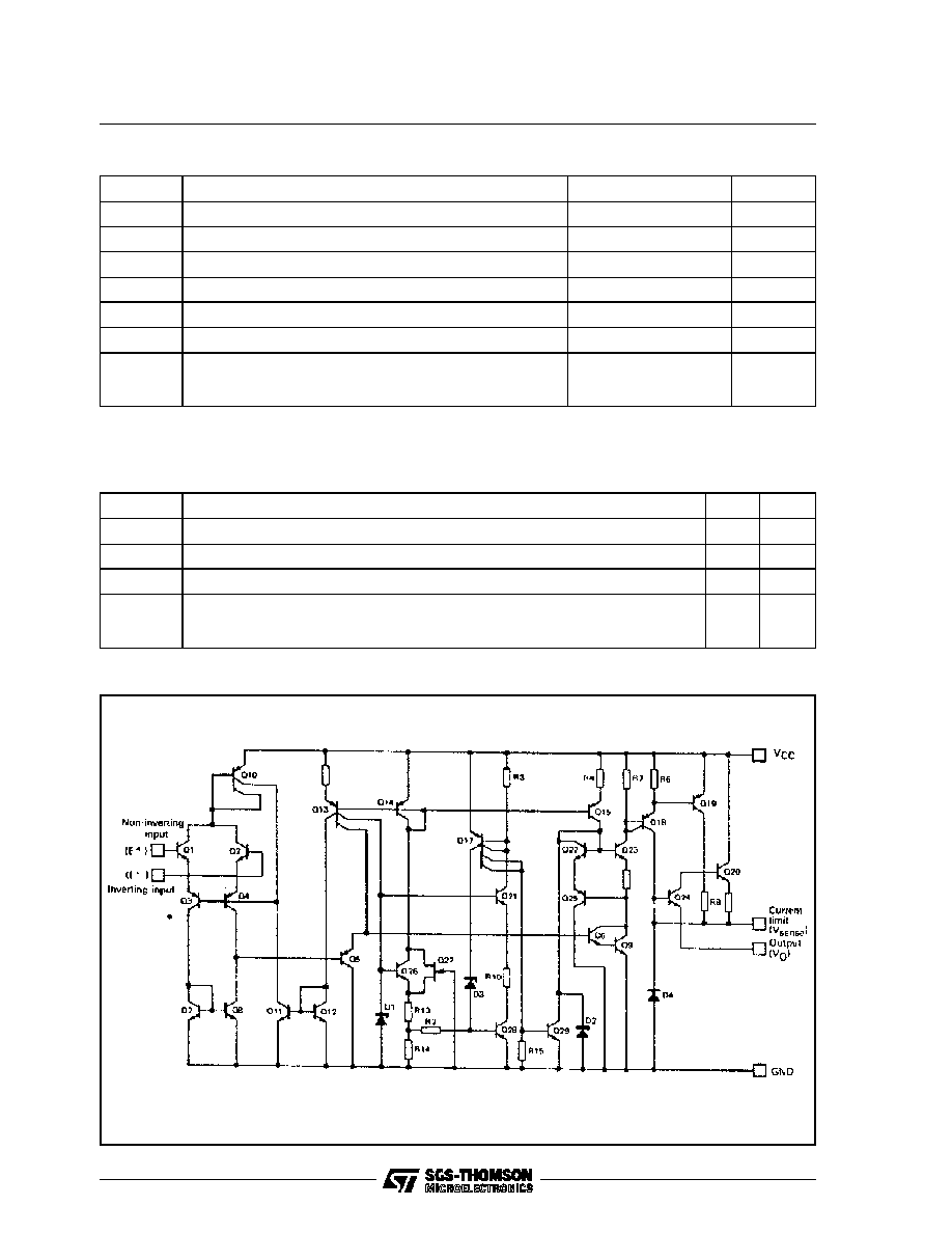
SCHEMATIC DIAGRAM
THERMAL CHARACTERISTICS
Symbol
Parameter
Value
Unit
R
th(j-c)
Maximum Junction-case Thermal Resistance
50
∞
C/W
R
th (j-a)
Maximum Junction-ambient Thermal Resistance
120
∞
C/W
R
th
Junction-ceramic Substrate (case glued to substrate)
SO14
90
∞
C/W
R
th
Junction-ceramic Substrate (case glued to substrate, substrate temperature
maintened constant)
SO14
65
∞
C/W
TDE1747 - TDF1747
2/11
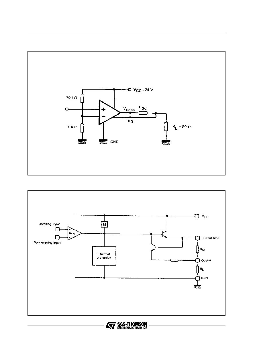
SIMPLIFIED CIRCUIT
TEST CIRCUIT
TDE1747 - TDF1747
3/11
ELECTRICAL CHARACTERISTICS T
j
= ≠ 25 to +85
∞
C, V
CC
= 8 to 45 V, unless otherwise specified
(note 1).
Symbol
Parameter
Min.
Typ.
Max.
Unit
V
IO
Input Offset Voltage - (note 2)
≠
2
50
mV
I
IB
Input Bias Current
≠
0.1
1.5
mA
I
CC
Supply Current (V
CC
= + 24 V, I
O
= 0)
High Level
Low Level
≠
≠
4
2
6
4
mA
mA
V
I(max)
Common-mode Input Voltage Range
2
≠
V
CC
≠2
V
I
SC
Short-circuit Current Limit
(T
amb
= + 25
∞
C, V
CC
= + 24)
R
SC
= 1.5
TDE1747
R
SC
=
≠
≠
480
35
≠
50
mA
mA
V
CC
≠V
O
Output Saturation Voltage (output high)
(R
SC
= 0, V
I
+≠V
I
≠
50 mV)
I
O
= 300 mA, T
j
= + 25
∞
C
T
j
= + 150
∞
C
≠
≠
1.15
1.05
1.4
1.3
V
V
I
OL
Low Level Output Current
(V
O
= 0, V
CC
= + 24 V)
T
j
= + 25
∞
C
≠
0.01
10
µ
A
Notes :
1) For operating at high temperature, the TDE/TDF1747, must be derated based on a + 150 C maximum junction temperature and a
junction-ambient thermal resistance of 120
∞
C/W for Minidip and 100
∞
C/W for the SO14.
2) The offset voltage given is the maximum value of input voltage required to drive the output voltage within 2 V of the ground or the supply
voltage.
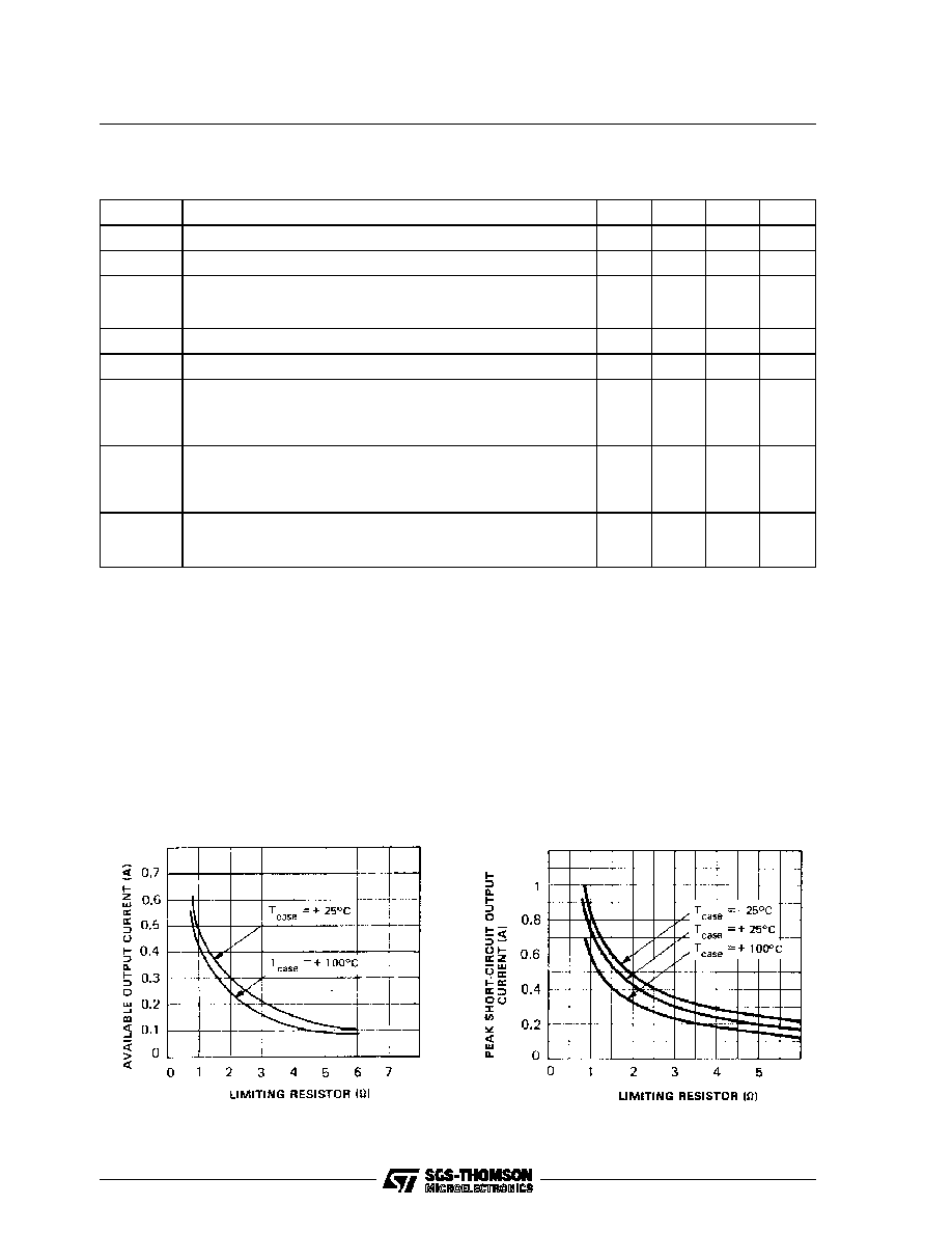
Figure 1: Available Output Current vs. Limiting
Resistor
Figure 2: Peak Short-circuit Output Current vs.
Limiting Resistor
TDE1747 - TDF1747
4/11
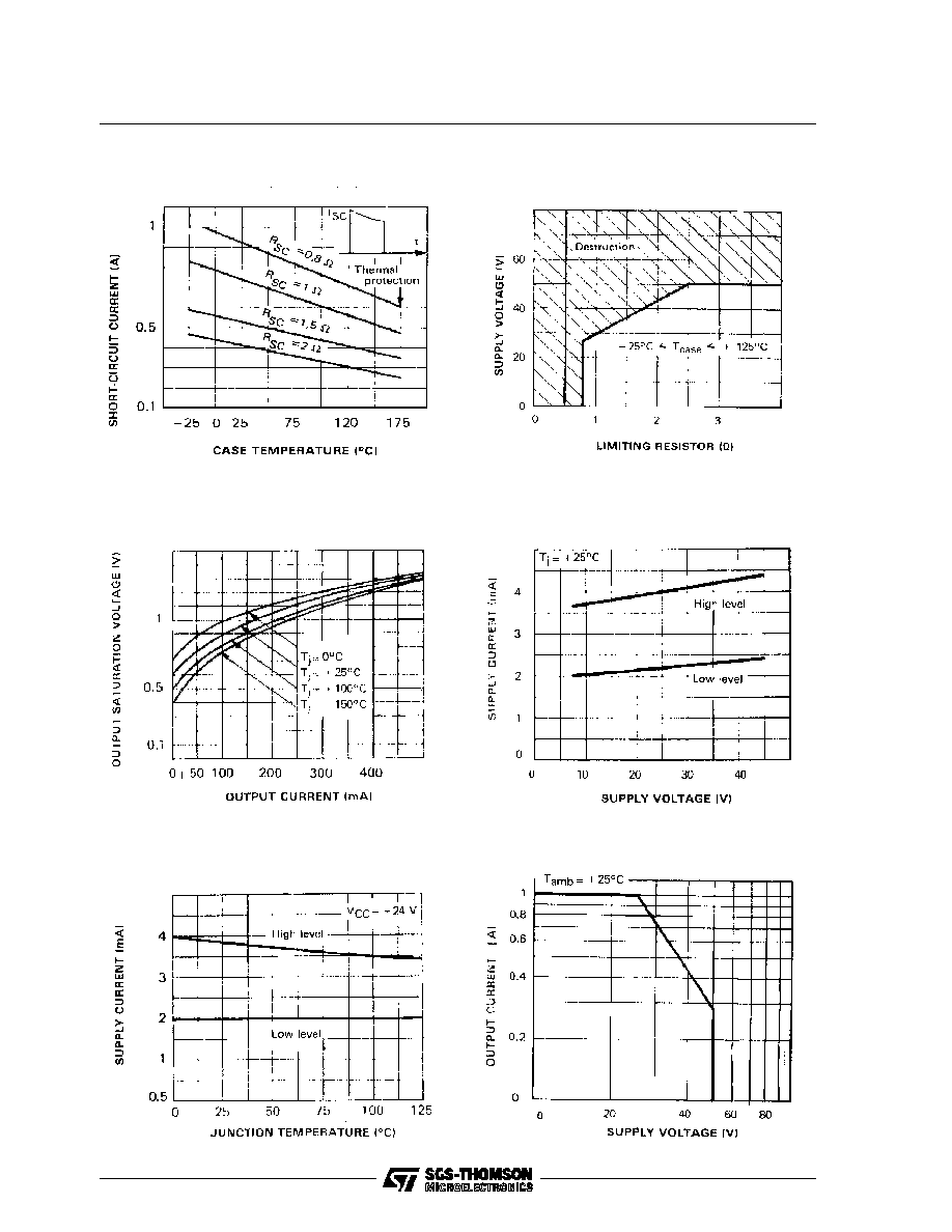
Figure 7: Supply Current vs. Junction
Temperature
Figure 8: Safe Operating Area (non repetitive
surge)
Figure 3: Short-circuit Current vs. Case
Temperature
Figure 4: Minimum Limiting Resistor Value vs.
Supply Voltage
Figure 5: Output Current vs. Output Saturation
Voltage
Figure 6: Supply Current vs. Supply Voltage
TDE1747 - TDF1747
5/11